PRELIMINARY DATA
This is preliminary information on a new product now in development or undergoing evaluation. Details are subject to
change without notice.
January 2006
Rev1.0
1/23
2
NAND01G-N
1 Gbit (x8/x16) 2112 Byte Page NAND Flash Memory and
512 Mbit (x16) LPSDRAM, 1.8V, Multi-Chip Package
Features summary
Multi-chip Package
≠ NAND Flash Memory
≠ 512 Mbit or 1 Gbit (x8/x16) Large Page
Size NAND Flash Memory
≠ 512 Mbit (x16) SDR or DDR LPSDRAM
Temperature range
≠ -30 up to 85 ∞C
Supply voltage
≠ NAND Flash : V
DDF
= 1.7V to 1.95V
≠ LPSDRAM: V
DDD
= V
DDQD
= 1.7V to 1.9V
Electronic Signature
ECOPACK
packages
Flash Memory
Nand Interface
≠ x8 or x16 bus width
≠ Multiplexed address/data
Page size
≠ x8 device: (2048 + 64 spare) Bytes
≠ x16 device: (1024 + 32 spare) Words
Block size
≠ x8 device: (128K + 4K spare) Bytes
≠ x16 device: (64K + 2K spare) Words
Page Read/Program
≠ Random access: 25µs (max)
≠ Sequential access: 50ns (min)
≠ Page program time: 300µs (typ)
Copy Back Program mode
≠ Fast page copy without external buffering
Fast Block Erase
≠ Block Erase time: 2ms (typ)
Chip Enable `don't care'
≠ for simple interfacing with microcontrollers
Status Register
SDR/DDR LPSDRAM
Interface: x16 bus width
Programmable Partial Array Self Refresh
Auto Temperature Compensated Self Refresh
Deep Power Down mode
1.8V LVCMOS interface
Quad internal Banks controlled by BA0 and
BA1
Wrap sequence: Sequential/Interleaved
Automatic and Controlled Precharge
Auto Refresh and Self Refresh
8,192 Refresh Cycles/64ms
Burst Termination by Burst Stop command and
Precharge Command
FBGA
TFBGA107 10.5 x 13 x 1.2mm
TFBGA149 10 x 13.5 x 1.2mm
www.st.com

NAND01G-N
2/23
Rev1.0
Table 1.
Product List
Reference
Part Number
NAND Product
LPSDRAM Product
(1)
Package
NAND01G-N
NAND01GR3N6
1Gbit 1.8V (x8)
SDR 512Mbit (x16) 1.8V, 133MHz
TFBGA107
NAND01GR4N5
1Gbit 1.8V (x16)
DDR 512Mbit (x16) 1.8V, 133 MHz
TFBGA149
1.
SDR = Single Data Rate; DDR = Double Data Rate.

NAND01G-N
Contents
Rev1.0
3/23
Contents
1
Summary description . . . . . . . . . . . . . . . . . . . . . . . . . . . . . . . . . . . . . . . . 7
NAND Flash component . . . . . . . . . . . . . . . . . . . . . . . . . . . . . . . . . . . . . . . . . . . . . 7
LPSDRAM component . . . . . . . . . . . . . . . . . . . . . . . . . . . . . . . . . . . . . . . . . . . . . . 7
2
Signals description . . . . . . . . . . . . . . . . . . . . . . . . . . . . . . . . . . . . . . . . . 12
2.1
Flash memory Inputs/Outputs (I/O0-I/O7) . . . . . . . . . . . . . . . . . . . . . . . . 12
2.2
Flash memory Inputs/Outputs (I/O8-I/O15) . . . . . . . . . . . . . . . . . . . . . . . 12
2.3
Flash memory Address Latch Enable (AL) . . . . . . . . . . . . . . . . . . . . . . . 12
2.4
Flash memory Command Latch Enable (CL) . . . . . . . . . . . . . . . . . . . . . . 12
2.5
Flash memory Chip Enable (EF) . . . . . . . . . . . . . . . . . . . . . . . . . . . . . . . 12
2.6
Flash memory Read Enable (R) . . . . . . . . . . . . . . . . . . . . . . . . . . . . . . . . 13
2.7
Flash memory Write Enable (WF) . . . . . . . . . . . . . . . . . . . . . . . . . . . . . . 13
2.8
Flash memory Write Protect (WP) . . . . . . . . . . . . . . . . . . . . . . . . . . . . . . 13
2.9
Flash memory Ready/Busy (RB) . . . . . . . . . . . . . . . . . . . . . . . . . . . . . . . 13
2.10
Flash memory V
DDF
supply voltage . . . . . . . . . . . . . . . . . . . . . . . . . . . . . 13
2.11
Flash memory V
SSF
ground . . . . . . . . . . . . . . . . . . . . . . . . . . . . . . . . . . . 13
2.12
LPSDRAM Address Inputs (A0-A12) . . . . . . . . . . . . . . . . . . . . . . . . . . . . 14
2.13
LPSDRAM Bank Select Address Inputs (BA0-BA1) . . . . . . . . . . . . . . . . . 14
2.14
LPSDRAM Data Inputs/Outputs (DQ0-DQ15) . . . . . . . . . . . . . . . . . . . . . 14
2.15
LPSDRAM Chip Select (ED) . . . . . . . . . . . . . . . . . . . . . . . . . . . . . . . . . . 14
2.16
LPSDRAM Column Address Strobe (CAS) . . . . . . . . . . . . . . . . . . . . . . . 14
2.17
LPSDRAM Row Address Strobe (RAS) . . . . . . . . . . . . . . . . . . . . . . . . . . 14
2.18
LPSDRAM Write Enable (WD) . . . . . . . . . . . . . . . . . . . . . . . . . . . . . . . . . 14
2.19
LPSDRAM Clock Input (K) . . . . . . . . . . . . . . . . . . . . . . . . . . . . . . . . . . . . 15
2.20
LPSDRAM Clock Input (K) . . . . . . . . . . . . . . . . . . . . . . . . . . . . . . . . . . . . 15
2.21
LPSDRAM Clock Enable (KE) . . . . . . . . . . . . . . . . . . . . . . . . . . . . . . . . . 15
2.22
LPSDRAM Lower/Upper Data Input/Output Mask (DQM0, DQM1) . . . . . 15
2.23
Lower/Upper Data Read/Write Strobe Input/Output (LDQS, UDQS) . . . . 15
2.24
LPSDRAM V
DDD
supply voltage . . . . . . . . . . . . . . . . . . . . . . . . . . . . . . . . 15
2.25
LPSDRAM V
DDQD
supply voltage . . . . . . . . . . . . . . . . . . . . . . . . . . . . . . 16
2.26
LPSDRAM V
SSD
ground . . . . . . . . . . . . . . . . . . . . . . . . . . . . . . . . . . . . . 16

Contents
NAND01G-N
4/23
Rev1.0
3
Functional description . . . . . . . . . . . . . . . . . . . . . . . . . . . . . . . . . . . . . . 17
4
Maximum rating . . . . . . . . . . . . . . . . . . . . . . . . . . . . . . . . . . . . . . . . . . . . 18
5
Package mechanical . . . . . . . . . . . . . . . . . . . . . . . . . . . . . . . . . . . . . . . . 19
6
Part numbering . . . . . . . . . . . . . . . . . . . . . . . . . . . . . . . . . . . . . . . . . . . . 21
7
Revision history . . . . . . . . . . . . . . . . . . . . . . . . . . . . . . . . . . . . . . . . . . . 22

NAND01G-N
List of tables
Rev1.0
5/23
List of tables
Table 1.
Product List . . . . . . . . . . . . . . . . . . . . . . . . . . . . . . . . . . . . . . . . . . . . . . . . . . . . . . . . . . . . . . 2
Table 2.
Signal Names . . . . . . . . . . . . . . . . . . . . . . . . . . . . . . . . . . . . . . . . . . . . . . . . . . . . . . . . . . . . 9
Table 3.
Absolute Maximum Ratings . . . . . . . . . . . . . . . . . . . . . . . . . . . . . . . . . . . . . . . . . . . . . . . . 18
Table 4.
TFBGA107 10.5x13mm - 10x14 active ball array, 0.80mm pitch, mechanical data . . . . . . 19
Table 5.
TFBGA149 10x13.5mm - 12x16 active ball array, 0.80mm pitch, mechanical data . . . . . . 20
Table 6.
Ordering Information Scheme. . . . . . . . . . . . . . . . . . . . . . . . . . . . . . . . . . . . . . . . . . . . . . . 21
Table 7.
Document Revision History . . . . . . . . . . . . . . . . . . . . . . . . . . . . . . . . . . . . . . . . . . . . . . . . 22

List of figures
NAND01G-N
6/23
Rev1.0
List of figures
Figure 1.
Logic Diagram. . . . . . . . . . . . . . . . . . . . . . . . . . . . . . . . . . . . . . . . . . . . . . . . . . . . . . . . . . . . 8
Figure 2.
TFBGA107 connections, x16 Bus Width (Top view through package) . . . . . . . . . . . . . . . . 10
Figure 3.
TFBGA149 Connections (Top view through package) . . . . . . . . . . . . . . . . . . . . . . . . . . . . 11
Figure 4.
Functional Block Diagram . . . . . . . . . . . . . . . . . . . . . . . . . . . . . . . . . . . . . . . . . . . . . . . . . . 17
Figure 5.
TFBGA107 10.5x13mm - 10x14 active ball array, 0.80mm pitch, package outline . . . . . . 19
Figure 6.
TFBGA149 10x13.5mm - 12x16 active ball array, 0.80mm pitch, package outline . . . . . . 20

NAND01G-N
Summary description
Rev1.0
7/23
1 Summary
description
The NAND01G-N is a family that combine two memory devices in a Multi-Chip Package: a 1
Gbit NAND Flash memory and 512 Mbit LPSDRAM with 2Kbyte Pages.
The NAND Flash memory and LPSDRAM components have separate power supplies and
grounds. They also have separate control, address and input/output signals, which allows
simultaneous access to both devices at any moment.
They are distinguished by two Chip Enable inputs: E
F
for the NAND Flash memory and E
D
for the LPSDRAM.
The Multi-Chip Packages are available with a 1.8V supply. See
Table 1
for a complete list of
the products available.
All devices are stacked and are offered in:
TFBGA107 (10.5 x 13 x 1.2mm)
TFBGA149 (10 x 13.5 x 1.2mm)
They are supplied with all the NAND Flash memory bits erased (set to `1').
This datasheet should be read in conjunction with the NAND Flash and LPSDRAM
datasheets.
NAND Flash component
NAND01G-N devices contain a 1 Gbit (x8/x16) 2112 Byte/1056 Word Page, NAND Flash
Memory. For detailed information on how to use the devices, see the NANDxxx-B datasheet
which is available from your local STMicroelectronics distributor.
LPSDRAM component
NAND01G-N devices contain a 512 Mbit (x16) LPSDRAM. For detailed information on how
to use the devices, see:
M65KA512AB: SDR 512Mb (x16)
M65KG512AB: DDR 512Mb (x16)
All above ST datasheets available from ST divisional Marketing.

Summary description
NAND01G-N
8/23
Rev1.0
Figure 1.
Logic Diagram
1.
Available on NAND01GR4N5 only.
AI10142d
13
A0-A12
DQ0-DQ15
V
SSQD
K
KE
W
D
V
DDQD
E
D
CAS
DQM1
DQM0
V
SSF
V
DDF
W
F
I/O8-I/O15, x16(1)
I/O0-I/O7, x8/x16
V
DDD
NAND01G-N
E
F
V
SSD
WP
AL
CL
RB
R
RAS
2
BA0-BA1
K(1)
UDQS-LDQS(1)
NAND01G-N
Summary description
Rev1.0
9/23
Table 2.
Signal Names
NAND Flash memory
I/O0-I/O7
Data Input/Outputs for x8 and x16 devices
I/O8-I/O15
Data Inputs/Outputs for x16 devices
AL
Address Latch Enable
CL
Command Latch Enable
E
F
Chip Enable
R
Read Enable
RB
Ready/Busy (open-drain output)
W
F
Write Enable
WP
Write Protect
V
DDF
Supply Voltage
V
SSF
Ground
LPSDRAM
A0-A12
Address Inputs
A10 determines the Precharge mode.
BA0-BA1
Bank Select Inputs
DQ0-DQ15
Data Inputs/Outputs
UDQS-LDQS
(1)
1.
Available on NAND01GR4N5 only.
Data Strobe Inputs/Outputs
K
Clock Input
K
(1)
Clock Input
KE
Clock Enable Input
E
D
Chip Select inputs
W
D
Write Enable Input
RAS
Row Address Strobe Input
CAS
Column Address Strobe Input
DQM0
DQ Mask Enable Input (controls DQ0-DQ7)
DQM1
DQ Mask Enable Input (controls DQ8-DQ15)
V
DDD
Supply Voltage
V
DDQD
Input/Output Supply Voltage
V
SSD
Ground
V
SSQD
Input/Output Ground
NC
Not Connected Internally
DU
Do Not Use
Summary description
NAND01G-N
10/23
Rev1.0
Figure 2.
TFBGA107 connections, x16 Bus Width (Top view through package)
AI10143c
VDDD
A8
DQM1
NC
VSSD
KE
A12
DQM0
H
A9
D
R
C
DQ4
A1
B
NC
A3
A
8
7
6
5
4
3
2
1
VSSD
VDDQD
G
F
E
VDDQD
DU
WP
A0
BA0
DQ6
VSSQD
CAS
A11
NC
WF
BA1
A10
DU
VDDD
VSSD
9
NC
A2
ED
M
L
K
J
DU
DQ15
NC
NC
DQ11
NC
I/O6
VDDQD
VSSQD
NC
DQ9
NC
I/O5
DQ13
VDDD
NC
NC
VSSF
VDDF
A7
I/O4
I/O7
A5
DU
DU
VSSQD
A4
DU
P
N
10
NC
RB
DQ2
NC
NC
EF
NC
I/O3
NC
VDDF
I/O2
NC
CL
AL
DQ0
VSSF
NC
I/O1
NC
VSSD
I/O0
K
NC
DQ1
DQ3
DQ5
DQ7
VDDD
DQ10
DQ12
DQ14
VSSF
DQ8
DU
DU
DU
DU
A6
WD
NC
RAS
VDDF
NC
NC

NAND01G-N
Summary description
Rev1.0
11/23
Figure 3.
TFBGA149 Connections (Top view through package)
AI11007c
DQM1
KE
A11
DQM0
H
A9
D
R
C
DQ4
A1
B
A3
A
8
7
6
5
4
3
2
1
G
F
E
DU
WP
A0
BA0
DQ6
CAS
WF
BA1
DU
VDDD
9
NC
A7
ED
M
L
K
J
DU
DQ15
NC
DQ13
VSSF
I/O0
I/O7
DU
DU
VSSQD
DU
P
N
12
NC
RB
DQ2
NC
NC
EF
I/O2
NC
CL
AL
DQ0
VSSD
I/O1
K
DQ1
DQ3
DQ5
DQ7
VDDD
DQ10
VSSD
DQ8
DU
DU
DU
DU
WD
NC
RAS
VDDF
NC
NC
NC
A10
DU
A8
DU
NC
DU
NC
VDDQD
NC
DU
DU
DU
DU
DU
DU
DU
DU
DU
DU
DU
DU
DU
DU
10
11
T
R
NC
DU
VSSD
VDDD
DU
NC
I/O6
I/O5
A6
A12
NC
NC
A2
A5
I/O4
NC
NC
A4
NC
VDDF
VSSF
NC
NC
NC
NC
NC
NC
NC
NC
NC
NC
NC
NC
NC
NC
NC
NC
NC
NC
NC
NC
I/O3
NC
DQ11
DQ14
DQ12
DQ9
VDDQD
VSSD
I/O9
I/O8
I/O15
I/O14
I/O13
I/O10
I/O12
I/O11
LDQS
UDQS
K

Signals description
NAND01G-N
12/23
Rev1.0
2 Signals
description
See
Figure 1
in conjunction with
Table 2
, for a brief overview of the signals connected to this
device.
For extra details on the signals, refer to the NAND Flash and the LPSDRAM datasheets.
2.1
Flash memory Inputs/Outputs (I/O0-I/O7)
Input/Outputs 0 to 7 are used by the NAND Flash memory to input the selected address,
output the data during a Read operation or input a command or data during a Write
operation. The inputs are latched on the rising edge of Write Enable. I/O0-I/O7 are left
floating when the NAND Flash memory is deselected or the outputs are disabled.
2.2
Flash memory Inputs/Outputs (I/O8-I/O15)
Input/Outputs 8 to 15 are only available in x16 NAND Flash devices. They are used to output
the data during a Read operation or input data during a Write operation. Command and
Address Inputs only require I/O0 to I/O7.
The inputs are latched on the rising edge of Write Enable. I/O8-I/O15 are left floating when
the device is deselected or the outputs are disabled.
2.3
Flash memory Address Latch Enable (AL)
The Address Latch Enable activates the latching of the Address inputs in the Command
Interface of the NAND Flash memory. When AL is high, the inputs are latched on the rising
edge of Write Enable.
2.4
Flash memory Command Latch Enable (CL)
The Command Latch Enable activates the latching of the Command inputs in the Command
Interface of the NAND Flash memory. When CL is high, the inputs are latched on the rising
edge of Write Enable.
2.5
Flash memory Chip Enable (E
F
)
The NAND Flash memory Chip Enable input activates the memory control logic, input
buffers, decoders and sense amplifiers. When Chip Enable is low, V
IL
, the NAND Flash
memory device is selected. If Chip Enable goes high, v
IH
, while the NAND Flash memory is
busy, the device remains selected and does not go into standby mode.

NAND01G-N
Signals description
Rev1.0
13/23
2.6
Flash memory Read Enable (R)
The NAND Flash memory Read Enable pin, R, controls the sequential data output during
Read operations. The falling edge of R also increments the internal column address counter
by one.
2.7
Flash memory Write Enable (W
F
)
The NAND Flash memory Write Enable input, W, controls writing to the Command Interface,
Input Address and Data latches. Both addresses and data are latched on the rising edge of
Write Enable.
2.8
Flash memory Write Protect (WP)
The Write Protect pin is a NAND Flash memory input that gives a hardware protection
against unwanted program or erase operations. When Write Protect is Low, V
IL
, the NAND
Flash memory device does not accept any program or erase operations.
It is recommended to keep the Write Protect pin Low, V
IL
, during power-up and power-down.
2.9
Flash memory Ready/Busy (RB)
The Ready/Busy output, RB, is an open-drain NAND Flash memory output that can be used
to identify if the P/E/R Controller is currently active.
When Ready/Busy is Low, V
OL
, a read, program or erase operation is in progress. When the
operation completes Ready/Busy goes High, V
OH
.
The use of an open-drain output allows the Ready/Busy pins from several memories to be
connected to a single pull-up resistor. A Low will then indicate that one, or more, of the
memories is busy.
2.10
Flash memory V
DDF
supply voltage
V
DDF
provides the power supply to the internal core of the NAND Flash memory device. It is
the main power supply for all operations (read, program and erase).
2.11
Flash memory V
SSF
ground
Ground, V
SSF,
is the reference for the power supply for the NAND Flash memory. It must be
connected to the system ground.

Signals description
NAND01G-N
14/23
Rev1.0
2.12
LPSDRAM Address Inputs (A0-A12)
The A0-A12 Address Inputs are used by the LPSDRAM to select the row or column to be
made active. If a row is selected, all thirteen, A0-A12 Address Inputs are used. If a column is
selected, only the nine least significant Address Inputs, A0-A8, are used. In this latter case,
A10 determines whether Auto Precharge is used. If A10 is High (set to `1') during Read or
Write, the Read or Write operation includes an Auto Precharge cycle. If A10 is Low (set to
`0') during Read or Write, the Read or Write cycle does not include an Auto Precharge cycle.
2.13
LPSDRAM Bank Select Address Inputs (BA0-BA1)
The BA0 and BA1 Banks Select Address Inputs are used by the LPSDRAM to select the
bank to be made active.
The LPSDRAM must be enabled, the Row Address Strobe, RAS, must be Low, V
IL
, the
Column Address Strobe, CAS, and W must be High, V
IH
, when selecting the addresses.
2.14
LPSDRAM Data Inputs/Outputs (DQ0-DQ15)
On the LPSDRAM, DQ0-DQ15 output the data stored at the selected address during a
Read operation, or are used to input the data during a write operation.
2.15
LPSDRAM Chip Select (E
D
)
The Chip Select input E activates the LPSDRAM state machine, address buffers and
decoders when driven Low, V
IL
. When High, V
IH
the device is not selected.
2.16
LPSDRAM Column Address Strobe (CAS)
The Column Address Strobe, CAS, is used in conjunction with Address Inputs A8-A0 and
BA1-BA0, to select the starting column location prior to a Read or Write.
2.17
LPSDRAM Row Address Strobe (RAS)
The Row Address Strobe, RAS, is used in conjunction with Address Inputs A11-A0 and
BA1-BA0, to select the starting address location prior to a Read or Write.
2.18
LPSDRAM Write Enable (W
D
)
The LPSDRAM Write Enable input, W, controls writing to the LPSDRAM.

NAND01G-N
Signals description
Rev1.0
15/23
2.19
LPSDRAM Clock Input (K)
The Clock signal, K, is used to clock the Read and Write cycles on the LPSDRAM. During
normal operation, the Clock Enable pin, KE, is High, V
IH
. The clock signal K can be
suspended to switch the device to the Self-Refresh, Power-Down or Deep Power-Down
mode by driving KE Low, V
IL
.
2.20
LPSDRAM Clock Input (K)
The Clock signal, K, is only available on the DDR LPSDRAM. It is used in conjunction with
the Clock signal, K.
All LPSDRAM input signals except DQM0/DQM1, UDQS/LDQS and DQ0-DQ15 are
referred to the cross point of K rising edge and K falling edge.
2.21
LPSDRAM Clock Enable (KE)
The Clock Enable, KE, pin is used by the LPSDRAM to control the synchronizing of the
signals with Clock signal K (and K on DDR LPSDRAM). If KE is High, V
IH
, the next Clock
rising edge is valid. When KE is Low, V
IL
, the signals are no longer clocked and data Read
and Write cycles are extended. KE is also involved in switching the device to the Self-
Refresh, Power-Down and Deep Power-Down modes.
2.22
LPSDRAM Lower/Upper Data Input/Output Mask (DQM0,
DQM1)
Data Mask Enable Inputs are used to mask the Read or Write data.
2.23
Lower/Upper Data Read/Write Strobe Input/Output (LDQS,
UDQS)
LDQS and UDQS are only available on the DDR LPSDRAM. They can be either input or
output signals and act as write data strobe and read data strobe respectively. LDQS and
UDQS are the strobe signals for DQ0 to DQ7 and DQ8 to DQ15, respectively.
2.24 LPSDRAM
V
DDD
supply voltage
V
DDD
provides the power supply to the internal core of the LPSDRAM. It is the main power
supply for all operations (Read and Write).

Signals description
NAND01G-N
16/23
Rev1.0
2.25 LPSDRAM
V
DDQD
supply voltage
V
DDQD
provides the power supply to the I/O pins of the LPSDRAM and enables all Outputs
to be powered independently of V
DDD
. V
DDQD
can be tied to V
DDD
or can use a separate
supply.
It is recommended to power-up and power-down V
DDD
and V
DDQD
together to avoid certain
conditions that would result in data corruption.
2.26 LPSDRAM
V
SSD
ground
Ground, V
SSD,
is the reference for the core power supply for the LPSDRAM. It must be
connected to the system ground.
NAND01G-N
Functional description
Rev1.0
17/23
3 Functional
description
The NAND Flash memory and LPSDRAM components have separate power supplies and
grounds. They also have separate control signals, addresses and data input/outputs, which
allows simultaneous access to both devices at any moment.
Figure 4.
Functional Block Diagram
1.
Available on Root Part Number 2 only.
V
SSD
WP
1 Gbit
NAND Flash
Memory
V
DDF
AL
W
D
CAS
RAS
LPSDRAM
V
DDD
DQM0
DQM1
BA0-BA1
Ai12401
E
D
I/O0-I/O7
CL
E
F
R
W
F
I/O8-I/O15
RB
V
SSF
V
DDQD
A0-A12
K
K(1)
KE
V
SSQD
DQ0-DQ15
LDQS-UDQS (1)
Maximum rating
NAND01G-N
18/23
Rev1.0
4 Maximum
rating
Stressing the device above the rating listed in the Absolute Maximum Ratings table may
cause permanent damage to the device. These are stress ratings only and operation of the
device at these or any other conditions above those indicated in the Operating sections of
this specification is not implied. Exposure to Absolute Maximum Rating conditions for
extended periods may affect device reliability. Refer also to the STMicroelectronics SURE
Program and other relevant quality documents.
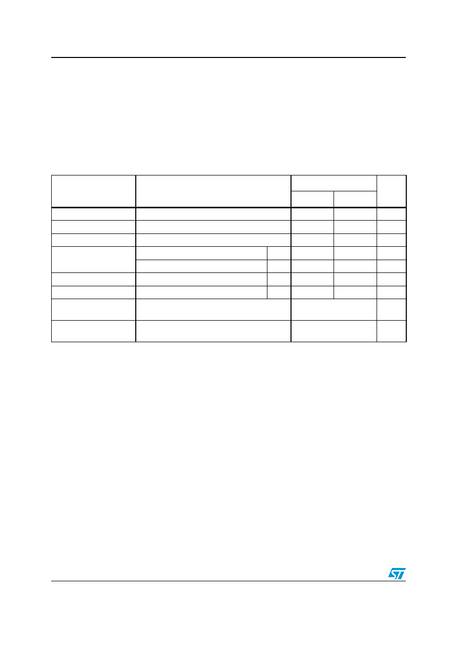
Table 3.
Absolute Maximum Ratings
Symbol
Parameter
Value
Unit
Min
Max
T
A
Ambient Operating Temperature
-30
85
∞C
T
BIAS
Temperature Under Bias
(1)
TBD
TBD
∞C
T
STG
Storage Temperature
-55
125
∞C
V
IO
NAND Flash Input or Output Voltage
1.8V
-0.6
2.7
V
LPSDRAM Input or Output Voltage
1.8V
-1.0
2.6
V
V
DDF
NAND Flash Supply Voltage
1.8V
-0.6
2.7
V
V
DDD
, V
DDQD
LPSDRAM Supply Voltage
1.8V
-1.0
2.6
V
LPSDRAM Short Circuit
Output Current
I
OS
50
mA
LPSDRAM Power
Dissipation
PD
1
W
1.
TBD stands for `To Be Determined'.

NAND01G-N
Package mechanical
Rev1.0
19/23
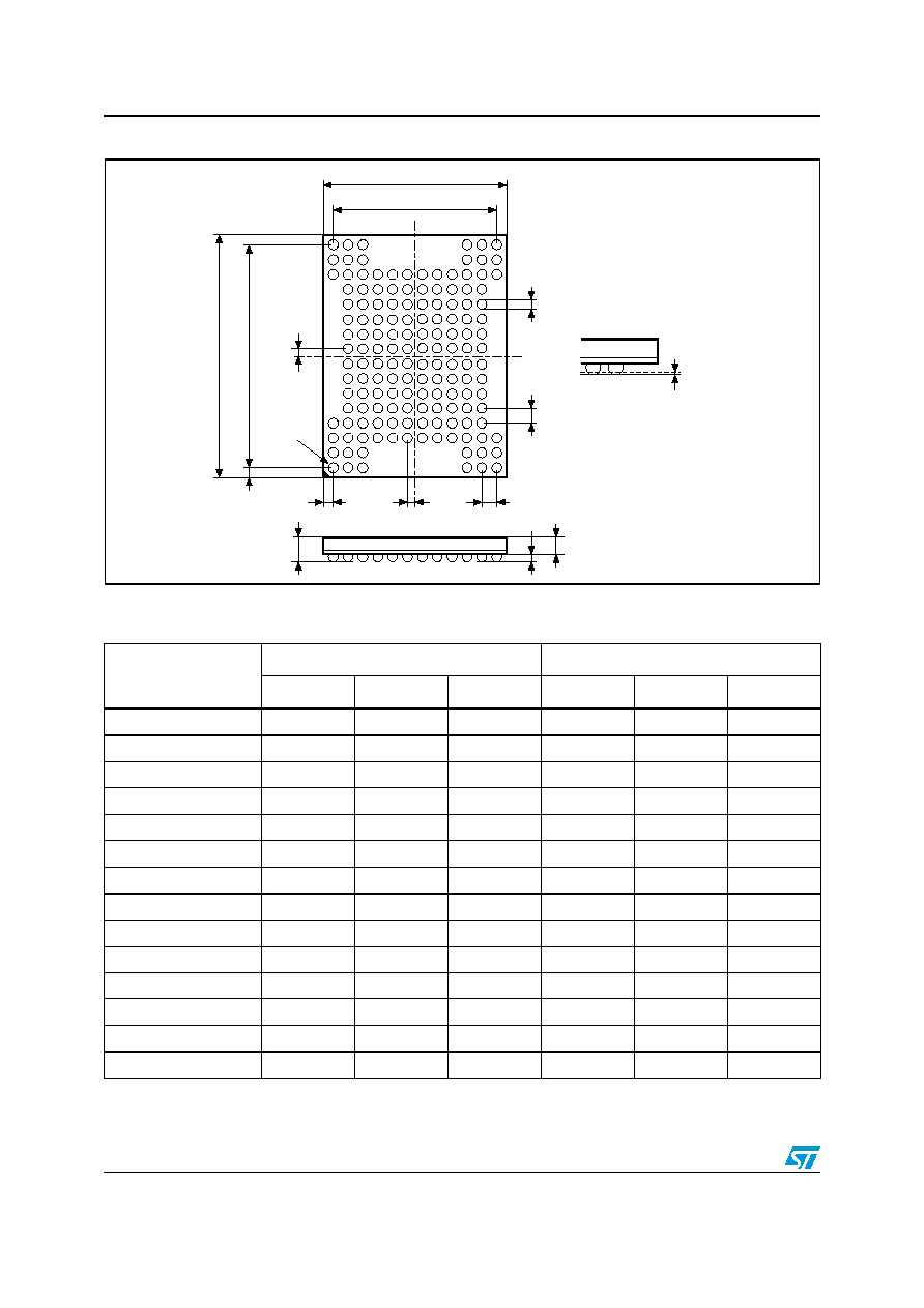
5 Package
mechanical
Figure 5.
TFBGA107 10.5x13mm - 10x14 active ball array, 0.80mm pitch, package outline
A2
A1
A
BGA-Z24
ddd
D
E
e
b
SE
FD
FE
E1
e
SD
D1
BALL "B1"
Table 4.
TFBGA107 10.5x13mm - 10x14 active ball array, 0.80mm pitch, mechanical data
Symbol
millimeters
inches
Typ
Min
Max
Typ
Min
Max
A
1.20
0.047
A1
0.25
0.010
A2
0.80
0.031
b
0.45
0.40
0.50
0.018
0.016
0.020
D
10.50
10.40
10.60
0.413
0.409
0.417
D1
7.20
0.283
ddd
0.10
0.004
E
13.00
12.90
13.10
0.512
0.508
0.516
E1
10.40
0.409
e
0.80
≠
≠
0.031
≠
≠
FD
1.65
0.065
FE
1.30
0.051
SD
0.40
0.016
SE
0.40
0.016
Package mechanical
NAND01G-N
20/23
Rev1.0
Figure 6.
TFBGA149 10x13.5mm - 12x16 active ball array, 0.80mm pitch, package outline
1.
Drawing not to scale.
A2
A1
A
BGA-Z78
ddd
D
E
e
b
SE
FD
FE
E1
e
SD
D1
BALL "A1"
Table 5.
TFBGA149 10x13.5mm - 12x16 active ball array, 0.80mm pitch, mechanical data
Symbol
millimeters
inches
Typ
Min
Max
Typ
Min
Max
A
1.200
0.0472
A1
0.250
0.0098
A2
0.800
0.0315
b
0.450
0.400
0.500
0.0177
0.0157
0.0197
D
10.000
9.900
10.100
0.3937
0.3898
0.3976
D1
8.800
0.3465
ddd
0.100
0.0039
E
13.500
13.400
13.600
0.5315
0.5276
0.5354
E1
12.000
0.4724
e
0.800
≠
≠
0.0315
≠
≠
FD
0.600
0.0236
FE
0.750
0.0295
SD
0.400
≠
≠
0.0157
≠
≠
SE
0.400
≠
≠
0.0157
≠
≠

NAND01G-N
Part numbering
Rev1.0
21/23
6 Part
numbering
Devices are shipped from the factory with the Flash memory content bits, in valid blocks,
erased to '1'. For further information on any aspect of this device, please contact your
nearest ST Sales Office.
Table 6.
Ordering Information Scheme
Example:
NAND01G R
3
N
6
A
ZB
5
E
Device Type
NAND Flash Memory
NAND Flash Density
01G = 1Gb
NAND Flash Operating Voltage
R = 1.7V to 1.95V
Bus Width
3 = x8
4 = x16
Family Identifier
N = 2112 Byte Page NAND Flash + LPSDRAM
Device Options
5 = DDR LPSDRAM 512Mbit (x16), 133 Mhz, BGA149
6 = SDR LPSDRAM 512Mbit (x 16), 133Mhz, BGA107
Product Version
A
Package
ZB = TFBGA
ZC = LFBGA
Reserved
Option
E = ECOPACK Package, Standard Packing
F = ECOPACK Package, Tape & Reel Packing

Revision history
NAND01G-N
22/23
Rev1.0
7 Revision
history
Table 7.
Document Revision History
Date
Version
Revision Details
18-Oct-2004
0.1
First Issue
19-Oct-2004
0.2
Figure 1: Logic Diagram
modified.
Table 1: Product List
modified.
26-Oct-2005
0.3
NAND512-N device removed from the document.TFBGA137 packages
removed from document. SDR 256Mb (x32) and SDR 512Mb (x32)
devices removed from document. NAND01GR3N3 removed throughout
document.
LDQM and UDQM replaced respectively by DQM0 and DQM1throughout
document.
DRAM changed to LPSDRAM throughout document.
LFBGA107 added throughout document. NAND01GR3N1,
NAND01GR3N2, NAND01GR3N6, NAND01GR4N5 added throughout
document.
31-Jan-2006
1.0
Note 1 below
Table 2: Signal Names
and
Figure 1: Logic Diagram
added
to cover both part numbers.
Figure 2: TFBGA107 connections, x16 Bus Width (Top view through
package)
and
Figure 3: TFBGA149 Connections (Top view through
package)
updated.
Section 2: Signals description
and
Section 3: Functional description
added.
256Mb LPSDRAM removed.
LFBGA107 (12 x 13 x 1.4mm) and LFBGA149 (10 x 13.5 x 1.4mm)
replaced by TFBGA107 (10.5x13x1.2mm) and TFBGA149
(10x13.5x1.2mm), respectively.

NAND01G-N
23/23
Please Read Carefully:
Information in this document is provided solely in connection with ST products. STMicroelectronics NV and its subsidiaries ("ST") reserve the
right to make changes, corrections, modifications or improvements, to this document, and the products and services described herein at any
time, without notice.
All ST products are sold pursuant to ST's terms and conditions of sale.
Purchasers are solely responsible for the choice, selection and use of the ST products and services described herein, and ST assumes no
liability whatsoever relating to the choice, selection or use of the ST products and services described herein.
No license, express or implied, by estoppel or otherwise, to any intellectual property rights is granted under this document. If any part of this
document refers to any third party products or services it shall not be deemed a license grant by ST for the use of such third party products
or services, or any intellectual property contained therein or considered as a warranty covering the use in any manner whatsoever of such
third party products or services or any intellectual property contained therein.
UNLESS OTHERWISE SET FORTH IN ST'S TERMS AND CONDITIONS OF SALE ST DISCLAIMS ANY EXPRESS OR IMPLIED
WARRANTY WITH RESPECT TO THE USE AND/OR SALE OF ST PRODUCTS INCLUDING WITHOUT LIMITATION IMPLIED
WARRANTIES OF MERCHANTABILITY, FITNESS FOR A PARTICULAR PURPOSE (AND THEIR EQUIVALENTS UNDER THE LAWS
OF ANY JURISDICTION), OR INFRINGEMENT OF ANY PATENT, COPYRIGHT OR OTHER INTELLECTUAL PROPERTY RIGHT.
UNLESS EXPRESSLY APPROVED IN WRITING BY AN AUTHORIZE REPRESENTATIVE OF ST, ST PRODUCTS ARE NOT DESIGNED,
AUTHORIZED OR WARRANTED FOR USE IN MILITARY, AIR CRAFT, SPACE, LIFE SAVING, OR LIFE SUSTAINING APPLICATIONS,
NOR IN PRODUCTS OR SYSTEMS, WHERE FAILURE OR MALFUNCTION MAY RESULT IN PERSONAL INJURY, DEATH, OR
SEVERE PROPERTY OR ENVIRONMENTAL DAMAGE.
Resale of ST products with provisions different from the statements and/or technical features set forth in this document shall immediately void
any warranty granted by ST for the ST product or service described herein and shall not create or extend in any manner whatsoever, any
liability of ST.
ST and the ST logo are trademarks or registered trademarks of ST in various countries.
Information in this document supersedes and replaces all information previously supplied.
The ST logo is a registered trademark of STMicroelectronics. All other names are the property of their respective owners.
© 2006 STMicroelectronics - All rights reserved
STMicroelectronics group of companies
Australia - Belgium - Brazil - Canada - China - Czech Republic - Finland - France - Germany - Hong Kong - India - Israel - Italy - Japan -
Malaysia - Malta - Morocco - Singapore - Spain - Sweden - Switzerland - United Kingdom - United States of America
www.st.com