 | –≠–ª–µ–∫—Ç—Ä–æ–Ω–Ω—ã–π –∫–æ–º–ø–æ–Ω–µ–Ω—Ç: NE555N | –°–∫–∞—á–∞—Ç—å:  PDF PDF  ZIP ZIP |
July 1998
Æ
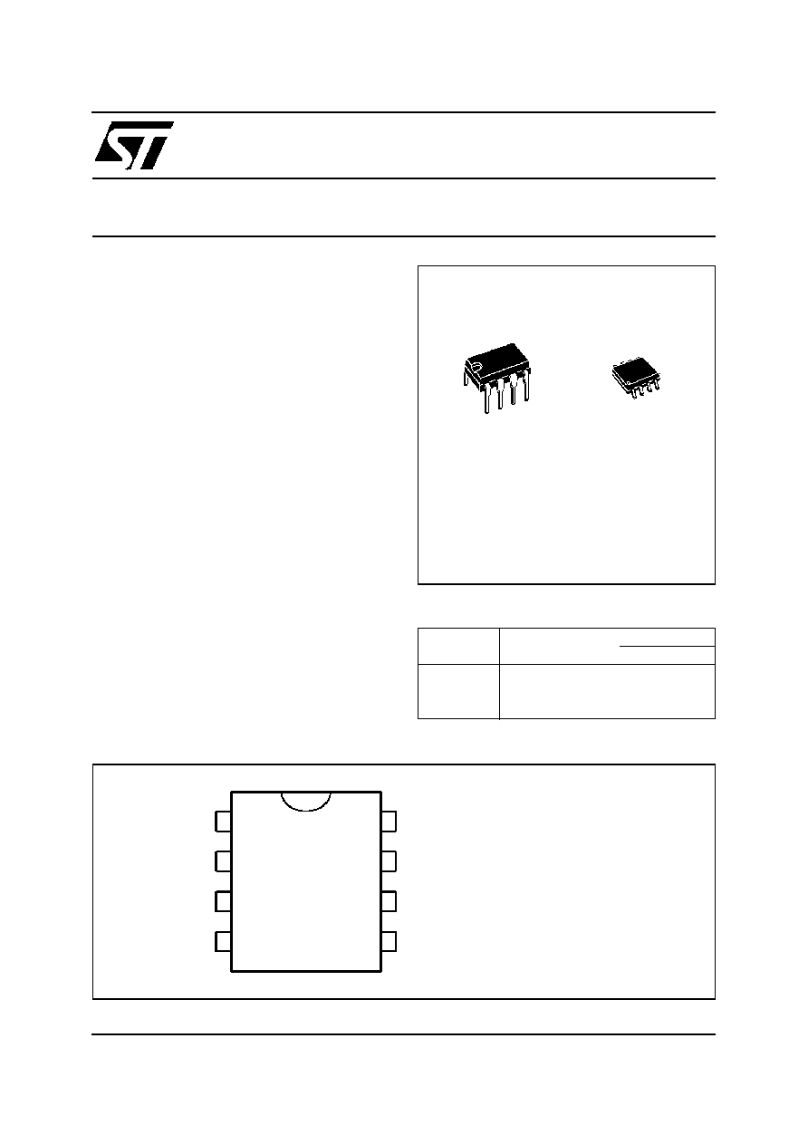
N
DIP8
(Plastic Package)
D
SO8
(Plastic Micropackage)
1
2
3
4
5
6
7
8
1 - GND
2 - Trigger
3 - Output
4 - Reset
5 - Control voltage
6 - Threshold
7 - Discharge
8 - V
CC
PIN CONNECTIONS (top view)
.
LOW TURN OFF TIME
.
MAXIMUM
OPERATING
FREQUENCY
GREATER THAN 500kHz
.
TIMING FROM MICROSECONDS TO HOURS
.
OPERATES
IN
BOTH
ASTABLE
AND
MONOSTABLE MODES
.
HIGH OUTPUT CURRENT CAN SOURCE OR
SINK 200mA
.
ADJUSTABLE DUTY CYCLE
.
TTL COMPATIBLE
.
TEMPERATURE
STABILITY
OF
0.005%
PER
o
C
ORDER CODES
Part
Number
Temperature
Range
Package
N
D
NE555
0
o
C, 70
o
C
∑
∑
SA555
≠40
o
C, 105
o
C
∑
∑
SE555
≠55
o
C, 125
o
C
∑
∑
DESCRIPTION
The NE555 monolithic timing circuit is a highly stable
controller capableof producing accuratetime delays
or oscillation. In the time delay mode of operation,
the time is precisely controlled by one external re-
sistor and capacitor.For a stableoperation as an os-
cillator, the free running frequency and the duty cy-
cle are both accurately controlled with two external
resistors and one capacitor. The circuit may be trig-
gered and reset on falling waveforms, and the out-
put structure can source or sink up to 200mA. The
NE555 is available in plastic and ceramic minidip
package and in a 8-lead micropackage and in metal
can package version.
NE555
SA555 - SE555
GENERAL PURPOSE SINGLE BIPOLAR TIMERS
1/10
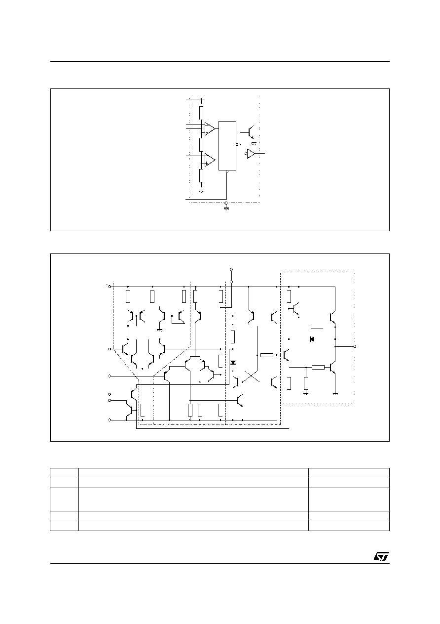
THRESHOLD
COMP
5k
5k
5k
TRIGGER
R
FLIP-FLOP
S
Q
DISCHARGE
OUT
INHIBIT/
RESET
RESET
COMP
S - 808 6
S
+
CONTROL VOLTAGE
V
CC
BLOCK DIAGRAM
OUTPUT
CONTROL
VOLTAGE
THRES HOLD
COMPARATOR
V
C C
R1
4.7k
R2
830
Q5
Q6
Q7
Q8
Q9
R3
4.7k
R 4
1k
R8
5k
Q1
Q2
Q3
Q4
Q10
Q11 Q12
Q13
THRES HOLD
TRIGGER
RES ET
DISC HARGE
G N D
2
4
7
1
Q14
Q15
R5
10k
R6
100k
R7
100k
R 10
5k
Q17
Q16
Q18
R 9
5k
D2
R 16
100
R15
4.7k
R 14
220
Q24
Q23
R17
4.7k
3
Q22
13
D1
Q19
Q20
Q21
R1 2
6.8k
5
TRIGGER COMPARATOR
F LIP F LOP
R11
5k
3.9k
SCHEMATIC DIAGRAM
ABSOLUTE MAXIMUM RATINGS
Symbol
Parameter
Value
Unit
V
cc
Supply Voltage
18
V
T
oper
Operating Free Air Temperature Range
for NE555
for SA555
for SE555
0 to 70
≠40 to 105
≠55 to 125
o
C
T
j
Junction Temperature
150
o
C
T
stg
Storage Temperature Range
≠65 to 150
o
C
NE555/SA555/SE555
2/10

ELECTRICAL CHARACTERISTICS
T
amb
= +25
o
C, V
CC
= +5V to +15V (unless otherwise specified)
Symbol
Parameter
SE555
NE555 - SA555
Unit
Min.
Typ.
Max.
Min.
Typ.
Max.
I
CC
Supply Current (R
L
) (- note 1)
Low State
V
CC
= +5V
V
CC
= +15V
High State
V
CC
= 5V
3
10
2
5
12
3
10
2
6
15
mA
Timing Error (monostable)
(R
A =
2k to 100k
, C = 0.1
µ
F)
Initial Accuracy - (note 2)
Drift with Temperature
Drift with Supply Voltage
0.5
30
0.05
2
100
0.2
1
50
0.1
3
0.5
%
ppm/
∞
C
%/V
Timing Error (astable)
(R
A
, R
B
= 1k
to 100k
, C = 0.1
µ
F,
V
CC
= +15V)
Initial Accuracy - (note 2)
Drift with Temperature
Drift with Supply Voltage
1.5
90
0.15
2.25
150
0.3
%
ppm/
∞
C
%/V
V
CL
Control Voltage level
V
CC
= +15V
V
CC
= +5V
9.6
2.9
10
3.33
10.4
3.8
9
2.6
10
3.33
11
4
V
V
th
Threshold Voltage
V
CC
= +15V
V
CC
= +5V
9.4
2.7
10
3.33
10.6
4
8.8
2.4
10
3.33
11.2
4.2
V
I
th
Threshold Current - (note 3)
0.1
0.25
0.1
0.25
µ
A
V
trig
Trigger Voltage
V
CC
= +15V
V
CC
= +5V
4.8
1.45
5
1.67
5.2
1.9
4.5
1.1
5
1.67
5.6
2.2
V
I
trig
Trigger Current (V
trig
= 0V)
0.5
0.9
0.5
2.0
µ
A
V
reset
Reset Voltage - (note 4)
0.4
0.7
1
0.4
0.7
1
V
I
reset
Reset Current
V
reset
= +0.4V
V
reset
= 0V
0.1
0.4
0.4
1
0.1
0.4
0.4
1.5
mA
V
OL
Low Level Output Voltage
V
CC
= +15V, I
O(sink)
= 10mA
I
O(sink)
= 50mA
I
O(sink)
= 100mA
I
O(sink)
= 200mA
V
CC
= +5V,
I
O(sink)
= 8mA
I
O(sink)
= 5mA
0.1
0.4
2
2.5
0.1
0.05
0.15
0.5
2.2
0.25
0.2
0.1
0.4
2
2.5
0.3
0.25
0.25
0.75
2.5
0.4
0.35
V
V
OH
High Level Output Voltage
V
CC
= +15V, I
O(source)
= 200mA
I
O(source)
= 100mA
V
CC
= +5V,
I
O(source)
= 100mA
13
3
12.5
13.3
3.3
12.75
2.75
12.5
13.3
3.3
V
Notes :
1. Supply current when output is high is typically 1mA less.
2. Tested at V
CC
= +5V and V
CC
= +15V.
3. This will determine the maximum value of R
A
+ R
B
for +15V operation the max total is R = 20M
and for 5V operation
the max total R = 3.5M
.
OPERATING CONDITIONS
Symbol
Parameter
SE555
NE555 - SA555
Unit
V
CC
Supply Voltage
4.5 to 18
4.5 to 18
V
V
th
, V
trig
, V
cl
, V
reset
Maximum Input Voltage
V
CC
V
CC
V
NE555/SA555/SE555
3/10
ELECTRICAL CHARACTERISTICS (continued)
Symbol
Parameter
SE555
NE555 - SA555
Unit
Min.
Typ.
Max.
Min.
Typ.
Max.
I
dis (off)
Discharge Pin Leakage Current
(output high) (V
dis
= 10V)
20
100
20
100
nA
V
dis(sat)
Discharge pin Saturation Voltage
(output low) - (note 5)
V
CC
= +15V, I
dis
= 15mA
V
CC
= +5V, I
dis
= 4.5mA
180
80
480
200
180
80
480
200
mV
t
r
t
f
Output Rise Time
Output Fall Time
100
100
200
200
100
100
300
300
ns
t
off
Turn off Time - (note 6) (V
reset
= V
CC
)
0.5
0.5
µ
s
Notes :
5. No protection against excessive Pin 7 current is necessary, providing the package dissipation rating will not be exceeded.
6. Time mesaured from a positive going input pulse from 0 to 0.8x V
CC
into the threshold to the drop from high to low of the
output trigger is tied to treshold.
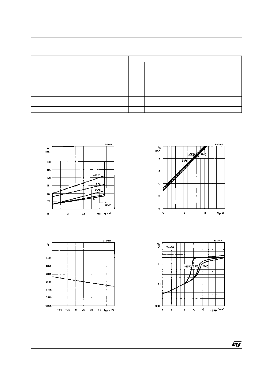
Figure 1 : Minimum Pulse Width Required for
Trigering
Figure 2 : Supply Current versus Supply Voltage
Figure 3 : Delay Time versus Temperature
Figure 4 : Low Output Voltage versus Output
Sink Current
NE555/SA555/SE555
4/10

Figure 5 : Low Output Voltage versus Output
Sink Current
Figure 6 : Low Output Voltage versus Output
Sink Current
Figure 7 : High Output Voltage Drop versus
Output
Figure 8 : Delay Time versus Supply Voltage
Figure 9 : Propagation Delay versus Voltage
Level of Trigger Value
NE555/SA555/SE555
5/10