 | –≠–ª–µ–∫—Ç—Ä–æ–Ω–Ω—ã–π –∫–æ–º–ø–æ–Ω–µ–Ω—Ç: P40NF03L | –°–∫–∞—á–∞—Ç—å:  PDF PDF  ZIP ZIP |
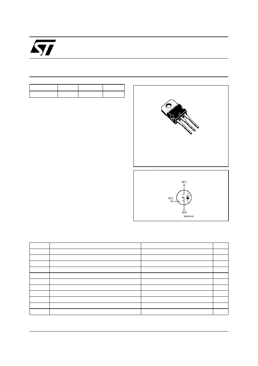
STP40NF03L
N - CHANNEL 30V - 0.020
- 40A TO-220
STripFET
TM
POWER MOSFET
s
TYPICAL R
DS(on)
= 0.020
s
LOW THRESHOLD DRIVE
DESCRIPTION
This Power MOSFET is the latest development of
STMicroelectronics
unique
"Single
Feature
Size
TM
"
strip-based
process.
The
resulting
transistor shows extremely high packing density
for
low
on-resistance,
rugged
avalanche
characteristics and less critical alignment steps
therefore
a
remarkable
manufacturing
reproducibility.
APPLICATIONS
s
HIGH CURRENT, HIGH SPEED SWITCHING
s
SOLENOID AND RELAY DRIVERS
s
MOTOR CONTROL, AUDIO AMPLIFIERS
s
DC-DC & DC-AC CONVERTERS
Æ
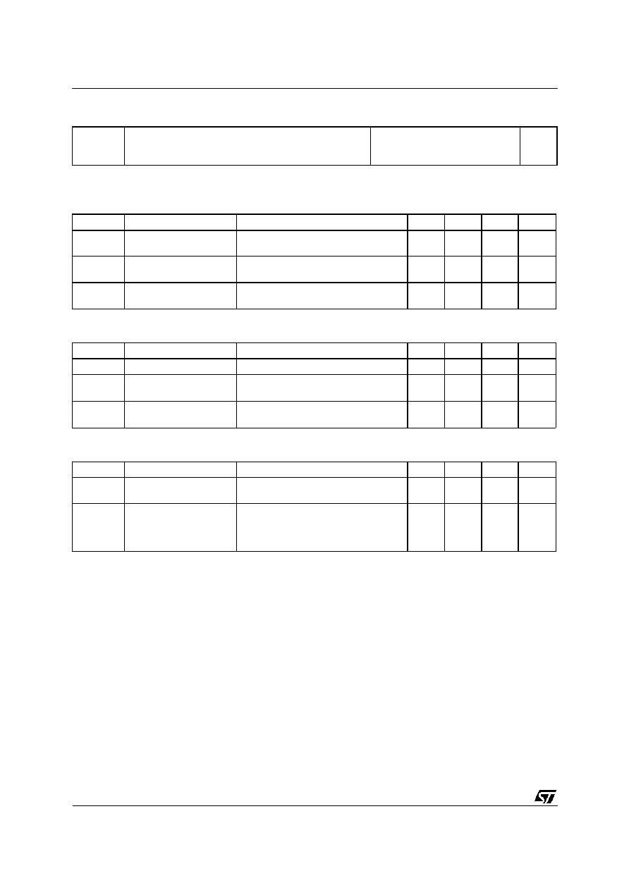
INTERNAL SCHEMATIC DIAGRAM
October 1999
ABSOLUTE MAXIMUM RATINGS
Symb ol
Parameter
Value
Unit
V
DS
Drain-source Voltage (V
GS
= 0)
30
V
V
DGR
Drain- gate Voltage (R
GS
= 20 k
)
30
V
V
G S
G ate-source Volt age
±
20
V
I
D
Drain Current (continuous) at T
c
= 25
o
C
40
A
I
D
Drain Current (continuous) at T
c
= 100
o
C
28
A
I
DM
(
∑)
Drain Current (pulsed)
160
A
P
tot
T otal Dissipation at T
c
= 25
o
C
70
W
Derating Factor
0.46
W /
o
C
E
AS
(
1
)
Single Pulse Avalanche Energy
250
m/ J
T
st g
Storage Temperature
-65 to 175
o
C
T
j
Max. Operating Junction Temperature
175
o
C
(
∑)
Pulse width limited by safe operating area
(
1
)
starting T
j
= 25
o
C, I
D
=20A , V
DD
= 15V
TYPE
V
DSS
R
DS(o n)
I
D
STP40NF03L
30 V
< 0.022
40 A
1
2
3
TO-220
1/8
THERMAL DATA
R
thj -case
R
thj -amb
T
l
Thermal Resistance Junction-case
Max
Thermal Resistance Junction-ambient
Max
Maximum Lead Temperature F or Soldering Purpose
2.1
62.5
300
o
C/W
o
C/W
o
C
ELECTRICAL CHARACTERISTICS (T
case
= 25
o
C unless otherwise specified)
OFF
Symbo l
Parameter
Test Con ditions
Min.
Typ.
Max.
Unit
V
(BR)DSS
Drain-source
Breakdown Voltage
I
D
= 250
µ
A
V
GS
= 0
30
V
I
DSS
Zero Gat e Voltage
Drain Current (V
GS
= 0)
V
DS
= Max Rat ing
V
DS
= Max Rat ing
T
c
=125
o
C
1
10
µ
A
µ
A
I
G SS
Gat e-body Leakage
Current (V
DS
= 0)
V
GS
=
±
20 V
±
100
nA
ON (
)
Symbo l
Parameter
Test Con ditions
Min.
Typ.
Max.
Unit
V
G S(th)
Gat e Threshold Voltage V
DS
= V
GS
I
D
= 250
µ
A
1
1.7
2. 5
V
R
DS(on)
Static Drain-source On
Resistance
V
GS
= 10 V
I
D
= 20 A
V
GS
= 4. 5 V
I
D
= 20 A
0.018
0.028
0.022
0.035
I
D(o n)
On State Drain Current
V
DS
> I
D(o n)
x R
DS(on )ma x
V
GS
= 10 V
40
A
DYNAMIC
Symbo l
Parameter
Test Con ditions
Min.
Typ.
Max.
Unit
g
f s
(
)
Forward
Transconductance
V
DS
> I
D(o n)
x R
DS(on )ma x
I
D
=20 A
20
S
C
iss
C
os s
C
rss
Input Capacitance
Out put Capacitance
Reverse Transfer
Capacitance
V
DS
= 25 V
f = 1 MHz
V
GS
= 0
830
230
92
pF
pF
pF
STP40NF03L
2/8

ELECTRICAL CHARACTERISTICS (continued)
SWITCHING ON
Symbo l
Parameter
Test Con ditions
Min.
Typ.
Max.
Unit
t
d(on)
t
r
Turn-on Delay T ime
Rise Time
V
DD
= 15 V
I
D
= 20 A
R
G
= 4.7
V
G S
= 4.5 V
(Resistive Load, see fig. 3)
35
205
ns
ns
Q
g
Q
gs
Q
gd
Tot al G ate Charge
Gat e-Source Charge
Gat e-Drain Charge
V
DD
= 24 V I
D
= 40 A V
GS
= 5 V
18
7
8
23
nC
nC
nC
SWITCHING OFF
Symbo l
Parameter
Test Con ditions
Min.
Typ.
Max.
Unit
t
d(of f)
t
f
Turn-off Delay T ime
Fall T ime
V
DD
= 15 V
I
D
= 20 A
R
G
= 4.7
V
G S
= 4.5 V
(Resistive Load, see fig. 3)
90
240
ns
ns
t
d(of f)
t
f
t
c
Off -volt age Rise T ime
Fall T ime
Cross-over Time
Vclamp = 24 V
I
D
= 20 A
R
G
= 4.7
V
G S
= 4.5 V
(Induct ive Load, see fig. 5)
150
155
340
ns
ns
ns
SOURCE DRAIN DIODE
Symbo l
Parameter
Test Con ditions
Min.
Typ.
Max.
Unit
I
SD
I
SDM
(
∑
)
Source-drain Current
Source-drain Current
(pulsed)
40
160
A
A
V
SD
(
)
Forward On Voltage
I
SD
= 40 A
V
GS
= 0
1. 5
V
t
rr
Q
rr
I
RRM
Reverse Recovery
Time
Reverse Recovery
Charge
Reverse Recovery
Current
I
SD
= 40 A
di/dt = 100 A/
µ
s
V
DD
= 15 V
T
j
= 150
o
C
(see t est circuit, f ig. 5)
65
72
2
ns
nC
A
(
) Pulsed: Pulse duration = 300
µ
s, duty cycle 1.5 %
(
∑
) Pulse width limited by safe operating area
Safe Operating Area
Thermal Impedance
STP40NF03L
3/8
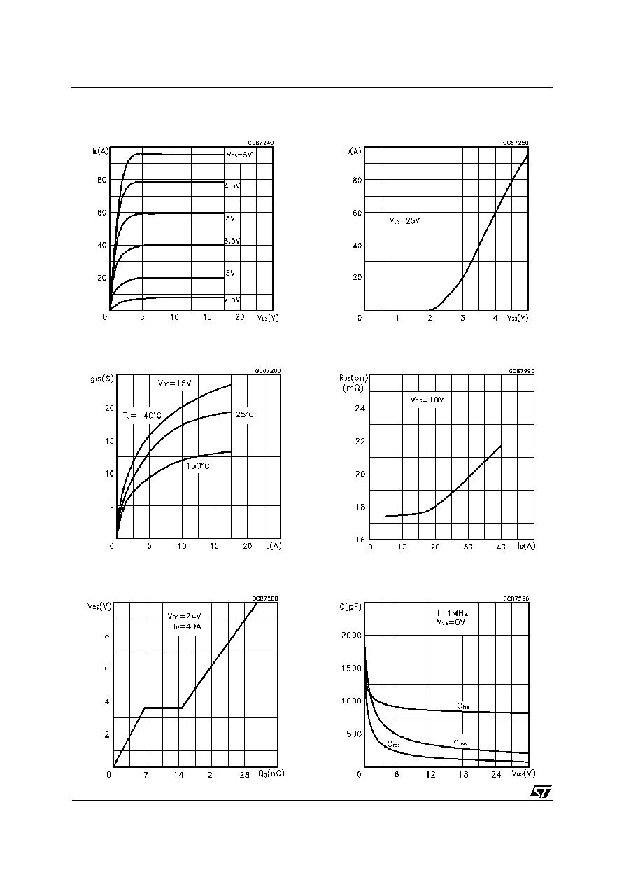
Output Characteristics
Transconductance
Gate Charge vs Gate-source Voltage
Transfer Characteristics
Static Drain-source On Resistance
Capacitance Variations
STP40NF03L
4/8

Normalized Gate Threshold Voltage vs
Temperature
Source-drain Diode Forward Characteristics
Normalized On Resistance vs Temperature
STP40NF03L
5/8