 | –≠–ª–µ–∫—Ç—Ä–æ–Ω–Ω—ã–π –∫–æ–º–ø–æ–Ω–µ–Ω—Ç: RBO08-40M | –°–∫–∞—á–∞—Ç—å:  PDF PDF  ZIP ZIP |

RBO08-40G/M/T
Æ
PowerSO-10
TM
RBO08-40M
8A DIODE TO GUARD AGAINST BATTERY RE-
VERSAL.
NEGATIVE OVERVOLTAGE PROTECTION BY
CLAMPING.
COMPLIANT WITH ISO/DTR 7637 STANDARD
FOR PULSES 1, 2, 3a and 3b.
SUITABLE FOR AUTOPROTECTED ALTER-
NATOR ENVIRONMENT.
BREAKDOWN VOLTAGE : 24 V min.
CLAMPING VOLTAGE :
±
40 V max.
MONOLITHIC STRUCTURE FOR GREATER
RELIABILITY.
FEATURES
Designed to protect against battery reversal and
overvoltages in automotiveapplications, this
monolithic component offers multiple functions in
the same package :
D1 : reversed battery protection
T1 : clamping against negative overvoltages
T2 : Transil function for overvoltage protection.
DESCRIPTION
FUNCTIONAL DIAGRAM
1
2
3
REVERSEDBATTERYAND
OVERVOLTAGEPROTECTIONCIRCUIT (RBO)
Application Specific Discretes
A.S.D.
TM
January 1998 - Ed : 2
D
2
PAK
RBO08-40G
TO220AB
RBO08-40T
1/14

Symbol
Parameter
Value
Unit
I
FSM
Non repetitive surge peak forward current
(Diode D1)
tp = 10 ms
80
A
I
F
DC forward current (Diode D1)
Tc = 75
∞
C
8
A
P
PP
Peak pulse power between Input and Output
(Transil T1)
see note 1 Tj initial = 25
∞
C
10/1000
µ
s
600
W
P
PP
Peak pulse power between Pins 3 and 2 (10/1000
µ
s)
1500
W
T
stg
Tj
Storage temperature range
Maximum junction temperature
- 40 to + 150
150
∞
C
T
L
Maximum lead temperature for soldering during 10 s
at 4.5mm from case for TO220AB
260
∞
C
Note 1 : for a surge greater than the maximum value, the device will fail in short-circuit..
TM : PowerSO-10, TRANSIL and ASD are trademarks of SGS-THOMSON Microelectronics.
ABSOLUTE MAXIMUM RATINGS
Symbol
Parameter
Value
Unit
Rth (j-c)
Junction to case
RBO08-40M
RBO08-40G
RBO08-40T
2.4
2.4
2.4
∞
C/W
THERMAL RESISTANCE
D1
T1
2
3
1
V
C L
31
V
R M
31
V
F
13
V13
I13
I
R M
31
I
R
31
Ipp31
V
B R
31
T2
I
F
Ipp32
V
R M
32 V
B R
32 V
C L
32
3
2
1
V32
I32
I
R
32
I
R M
32
Æ
RBO08-40G / RBO08-40M / RBO08-40T
2/14

Symbol
Test Conditions
Value
Unit
Min.
Typ.
Max.
V
F 13
I
F
= 8 A
RBO08-40M/G
1.5
V
RBO08-40T
1.7
V
I
F
= 8 A @ T
amb
= 25
∞
C
1.45
V
V
F 13
I
F
= 4 A
RBO08-40M/G
1.3
V
RBO08-40T
1.35
V
I
F
= 4 A @ T
amb
= 25
∞
C
1.2
V
V
F 13
I
F
= 1 A
1.1
V
I
F
= 1 A @ T
amb
= 25
∞
C
1.0
V
I
F
= 1 A @ Tj = 85
∞
C
0.9
V
ELECTRICAL CHARACTERISTICS : DIODE D1 (- 40
∞
C < T
amb
< + 85
∞
C)
Symbol
Parameter
V
RM31
/V
RM32
Stand-off voltage Transil T1 / Transil T2.
V
BR31
/V
BR32
Breakdown voltage Transil T1 / Transil T2.
I
R31
/I
R32
Leakage current Transil T1 / Transil T2.
V
CL31
/V
CL32
Clamping voltage Transil T1 / Transil T2.
V
F13
Forward voltage drop Diode D1.
I
PP
Peak pulse current.
T
Temperature coefficient of V
BR
.
C
31
/C
32
Capacitance Transil T1 / Transil T2.
Symbol
Test Conditions
Value
Unit
Min.
Typ.
Max.
V
BR 31
I
R
= 1 mA
22
35
V
V
BR 31
I
R
= 1 mA, T
amb
= 25
∞
C
24
32
V
I
RM 31
V
RM
= 20 V
50
µ
A
I
RM 31
V
RM
= 20 V, T
amb
= 25
∞
C
10
µ
A
V
CL 31
I
PP
= 15A, Tj initial = 25
∞
C
10/1000
µ
s
40
V
T
Temperature coefficient of V
BR
9
10
-4
/
∞
C
C
31
F = 1MHz
V
R
= 0 V
1000
pF
ELECTRICAL CHARACTERISTICS : TRANSIL T1 (- 40
∞
C < T
amb
< + 85
∞
C)
Symbol
Test Conditions
Value
Unit
Min.
Typ.
Max.
V
BR 32
I
R
= 1 mA
22
35
V
V
BR 32
I
R
= 1 mA, T
amb
= 25
∞
C
24
32
V
I
RM 32
V
RM
= 20 V
50
µ
A
I
RM 32
V
RM
= 20 V, T
amb
= 25
∞
C
10
µ
A
V
CL 32
IPP = 37.5 A
10/1000
µ
s
40
V
T
Temperature coefficient of V
BR
8.5
10
-4
/
∞
C
C
32
F = 1MHz
V
R
= 0 V
2000
pF
ELECTRICAL CHARACTERISTICS : TRANSIL T2 (- 40
∞
C < T
amb
< + 85
∞
C)
Æ
RBO08-40G / RBO08-40M / RBO08-40T
3/14

PRODUCT DESCRIPTION
1
2
3
The RBO has 3 functionsintegrated on the same
chip.
D1 : "Diode function" in order to protect against
reversed battery operation.
T2 : "Transil function" in order to protect against
positive surge generated by electric systems
(ignition, relay. ...).
T1 : Protection againt negative surges such as
inductive overvoltages (see motor application
below).
BASIC APPLICATION
* The mono lithic multi-function protection
(RBO) has be en developed to protect
sensitive semicond uctors in car electronic
modules against both overvoltage and
battery reverse.
* In addition, the RBO circuit prevents
overvoltages generated by the module from
affecting the car supply network.
MOTOR DRIVER APPLICATION
D1
T1
T2
BATTERY
RBO
DEVICE
MOTOR CONTROL
MOTOR
Filter
In this application, one half of the motor drive circuit is supplied through the "RBO" and is thus protected
as per its basic function application.
The second part is connected directly to the "car supply network" and is protected as follows :
- For positive surges : T2 (clamping phase) and D1 in forward-biased.
- For negative surges : T1 (clamping phase) and T2 in forward-biased.
Æ
RBO08-40G / RBO08-40M / RBO08-40T
4/14
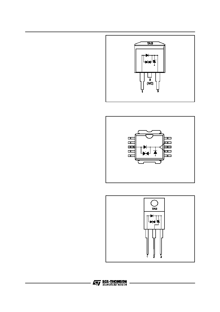
- Input
(1) : Pin 1
- Output (3) : Pin 3
- Gnd
(2) : Connected to base Tab
Marking
: Logo, date code, RBO08-40G
PINOUT configuration in D
2
PAK :
D1
T1
T2
TAB
D1
T1
T2
(TAB)
- Input
(1) : Pin 1
- Output (3) : Pin 3
- GND
(2) : Connected to base Tab
Marking
: Logo, date code, RBO08-40T
PINOUT configuration in TO220AB :
- Input
(1) : Pin 3
- Output (3) : Pin 7 and 9
- Gnd
(2) : Connected to base Tab
Marking
: Logo, date code, RBO08-40M
PINOUT configuration in PowerSO-10 :
TOP VIEW
Pin 1 (NC)
Input (1)
Gnd (2)
T1
D1
Tab
T2
Output (3)
Pin 2 (NC)
Pin 3 (Input 1)
Pin 4 (NC)
Pin 5 (NC)
Pin 10 (NC)
Pin 9 (Ouput 3)
Pin 8 (NC)
Pin 7 (Ouput 3)
Pin 6 (NC)
Æ
RBO08-40G / RBO08-40M / RBO08-40T
5/14