 | –≠–ª–µ–∫—Ç—Ä–æ–Ω–Ω—ã–π –∫–æ–º–ø–æ–Ω–µ–Ω—Ç: S1HNK60 | –°–∫–∞—á–∞—Ç—å:  PDF PDF  ZIP ZIP |

1/8
August 2003
STS1HNK60
N-CHANNEL 600V - 8
- 0.3A SO-8
SuperMESHTMPower MOSFET
s
TYPICAL R
DS
(on) = 8
s
EXTREMELY HIGH dv/dt CAPABILITY
s
100% AVALANCHE TESTED
s
GATE CHARGE MINIMIZED
s
NEW HIGH VOLTAGE BENCHMARK
DESCRIPTION
The SuperMESHTM series is obtained through an
extreme optimization of ST's well established strip-
based PowerMESHTM layout. In addition to pushing
on-resistance significantly down, special care is tak-
en to ensure a very good dv/dt capability for the
most demanding applications. Such series comple-
ments ST full range of high voltage MOSFETs in-
cluding revolutionary MDmeshTM products.
APPLICATIONS
s
SWITCH MODE LOW POWER SUPPLIES
(SMPS)
s
LOW POWER, LOW COST CFL (COMPACT
FLUORESCENT LAMPS)
s
LOW POWER BATTERY CHARGERS
ORDERING INFORMATION
TYPE
V
DSS
R
DS(on)
I
D
Pw
STS1HNK60
600 V
< 8.5
0.3 A
2 W
SALES TYPE
MARKING
PACKAGE
PACKAGING
STS1HNK60
S1HNK60
SO-8
TAPE & REEL
SO-8
INTERNAL SCHEMATIC DIAGRAM
STS1HNK60
2/8
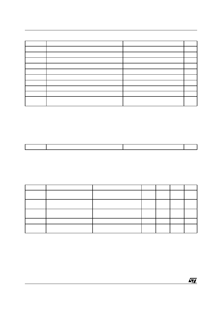
ABSOLUTE MAXIMUM RATINGS
( ) Pulse width limited by safe operating area
(1) I
SD
0.3A, di/dt
100A/µs, V
DD
V
(BR)DSS
, T
j
T
JMAX.
THERMAL DATA
ELECTRICAL CHARACTERISTICS (T
CASE
=25∞C UNLESS OTHERWISE SPECIFIED)
ON/OFF
Symbol
Parameter
Value
Unit
V
DS
Drain-source Voltage (V
GS
= 0)
600
V
V
DGR
Drain-gate Voltage (R
GS
= 20 k
)
600
V
V
GS
Gate- source Voltage
± 30
V
I
D
Drain Current (continuous) at T
C
= 25∞C
0.3
A
I
D
Drain Current (continuous) at T
C
= 100∞C
0.19
A
I
DM
( )
Drain Current (pulsed)
1.2
A
P
TOT
Total Dissipation at T
C
= 25∞C
2
W
Derating Factor
0.016
W/∞C
dv/dt (1)
Peak Diode Recovery voltage slope
3
V/ns
T
j
T
stg
Operating Junction Temperature
Storage Temperature
-65 to 150
∞C
Rthj-amb
Thermal Resistance Junction-ambient Max
62.5
∞C/W
Symbol
Parameter
Test Conditions
Min.
Typ.
Max.
Unit
V
(BR)DSS
Drain-source
Breakdown Voltage
I
D
= 1 mA, V
GS
= 0
600
V
I
DSS
Zero Gate Voltage
Drain Current (V
GS
= 0)
V
DS
= Max Rating
V
DS
= Max Rating, T
C
= 125 ∞C
1
50
µA
µA
I
GSS
Gate-body Leakage
Current (V
DS
= 0)
V
GS
= ± 30 V
±100
nA
V
GS(th)
Gate Threshold Voltage
V
DS
= V
GS
, I
D
= 250 µA
2.25
3
3.7
V
R
DS(on)
Static Drain-source On
Resistance
V
GS
= 10 V, I
D
= 0.5 A
8
8.5

3/8
STS1HNK60
ELECTRICAL CHARACTERISTICS (CONTINUED)
DYNAMIC
SWITCHING ON
SWITCHING OFF
SOURCE DRAIN DIODE
Note: 1. Pulsed: Pulse duration = 300 µs, duty cycle 1.5 %.
2. Pulse width limited by safe operating area.
Symbol
Parameter
Test Conditions
Min.
Typ.
Max.
Unit
g
fs
(1)
Forward Transconductance
V
DS
> I
D(on)
x R
DS(on)max,
I
D
= 0.5 A
1
S
C
iss
C
oss
C
rss
Input Capacitance
Output Capacitance
Reverse Transfer
Capacitance
V
DS
= 25V, f = 1 MHz, V
GS
= 0
156
23.5
3.8
pF
pF
pF
Symbol
Parameter
Test Conditions
Min.
Typ.
Max.
Unit
t
d(on)
t
r
Turn-on Delay Time
Rise Time
V
DD
= 300 V, I
D
= 0.5 A
R
G
= 4.7
V
GS
= 10 V
(Resistive Load see, Figure 3)
6.5
5
ns
ns
Q
g
Q
gs
Q
gd
Total Gate Charge
Gate-Source Charge
Gate-Drain Charge
V
DD
= 480 V, I
D
= 1 A,
V
GS
= 10V, R
G
= 4.7
7
1.1
3.4
10
nC
nC
nC
Symbol
Parameter
Test Conditions
Min.
Typ.
Max.
Unit
t
d(off)
t
f
Turn-off Delay Time
Fall Time
V
DD
= 300 V, I
D
= 0.5 A
R
G
= 4.7
V
GS
= 10 V
(Resistive Load see, Figure 3)
19
25
ns
ns
t
r(Voff)
t
f
t
c
Off-voltage Rise Time
Fall Time
Cross-over Time
V
DD
= 480V, I
D
= 1.0 A,
R
G
= 4.7
,
V
GS
= 10V
(Inductive Load see, Figure 5)
24
25
44
ns
ns
ns
Symbol
Parameter
Test Conditions
Min.
Typ.
Max.
Unit
I
SD
I
SDM
(2)
Source-drain Current
Source-drain Current (pulsed)
0.3
1.2
A
A
V
SD
(1)
Forward On Voltage
I
SD
= 0.3 A, V
GS
= 0
1.6
V
t
rr
Q
rr
I
RRM
Reverse Recovery Time
Reverse Recovery Charge
Reverse Recovery Current
I
SD
= 0.3 A, di/dt = 100 A/µs
V
DD
= 25 V, T
j
= 150∞C
(see test circuit, Figure 5)
229
377
3.3
ns
µC
A

STS1HNK60
4/8
Thermal Impedance
Static Drain-source On Resistance
Transconductance
Output Characteristics
Safe Operating Area
Transfer Characteristics

5/8
STS1HNK60
Normalized BVDSS vs Temperature
Normalized On Resistance vs Temperature
Normalized Gate Threshold Voltage vs Temp.
Gate Charge vs Gate-source Voltage
Capacitance Variations
Source-drain Diode Forward Characteristics

STS1HNK60
6/8
Fig. 5: Test Circuit For Inductive Load Switching
And Diode Recovery Times
Fig. 4: Gate Charge test Circuit
Fig. 2: Unclamped Inductive Waveform
Fig. 1: Unclamped Inductive Load Test Circuit
Fig. 3: Switching Times Test Circuit For
Resistive Load
7/8
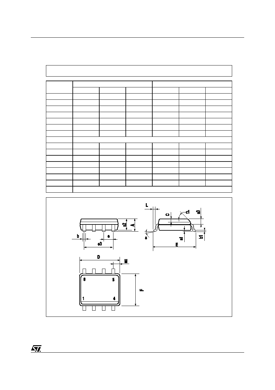
STS1HNK60
DIM.
mm
inch
MIN.
TYP.
MAX.
MIN.
TYP.
MAX.
A
1.75
0.068
a1
0.1
0.25
0.003
0.009
a2
1.65
0.064
a3
0.65
0.85
0.025
0.033
b
0.35
0.48
0.013
0.018
b1
0.19
0.25
0.007
0.010
C
0.25
0.5
0.010
0.019
c1
45 (typ.)
D
4.8
5.0
0.188
0.196
E
5.8
6.2
0.228
0.244
e
1.27
0.050
e3
3.81
0.150
F
3.8
4.0
0.14
0.157
L
0.4
1.27
0.015
0.050
M
0.6
0.023
S
8 (max.)
0016023
SO-8 MECHANICAL DATA
STS1HNK60
8/8
Information furnished is believed to be accurate and reliable. However, STMicroelectronics assumes no responsibility for the
consequences of use of such information nor for any infringement of patents or other rights of third parties which may result from
its use. No license is granted by implication or otherwise under any patent or patent rights of STMicroelectronics. Specifications
mentioned in this publication are subject to change without notice. This publication supersedes and replaces all information
previously supplied. STMicroelectronics products are not authorized for use as critical components in life support devices or
systems without express written approval of STMicroelectronics.
© The ST logo is a registered trademark of STMicroelectronics
© 2003 STMicroelectronics - Printed in Italy - All Rights Reserved
STMicroelectronics GROUP OF COMPANIES
Australia - Brazil - Canada - China - Finland - France - Germany - Hong Kong - India - Israel - Italy - Japan - Malaysia - Malta - Morocco
Singapore - Spain - Sweden - Switzerland - United Kingdom - United States.
© http://www.st.com