 | –≠–ª–µ–∫—Ç—Ä–æ–Ω–Ω—ã–π –∫–æ–º–ø–æ–Ω–µ–Ω—Ç: SBPH400-3 | –°–∫–∞—á–∞—Ç—å:  PDF PDF  ZIP ZIP |

16 March 1998
42 1697 05
The information in this datasheet is subject to change
Æ
SBPH400-3
IEEE1394 3-Port 400Mbps Physical Layer
PRELIMINARY DATA
s
FEATURES
s
3 ports fully compliant with IEEE 1394-1995
cable environment specification
s
Fully
implements
IEEE
P1394a
D2.0
proposal
s
S100, S200 and S400 speeds
s
IEEE P1394a proposal PHY-LINK interface
s
IEEE P1394a proposal Suspend/Resume
s
OHCI support
s
Per port disable
s
Automatic power saving
s
Optional isolation support
s
IEEE
P1394a
proposal
arbitration
enhancements
s
IEEE P1394a proposal register set and
remote register read
s
Advanced
Data-Strobe
clock
and
data
recovery
s
Digital
delay-lock
loop technology
- no
filtering capacitors
s
Built-in self-test (BIST) of analog and digital
port logic
s
JTAG Test Access Port
s
3.3V supply
s
80 pin plastic TQFP package
s
APPLICATIONS
s
Host processor interface
s
Host processor adapter cards
s
Digital set-top box
s
Digital Video Recorder/ Player
s
Repeaters
1394 cable
interface
@400 Mbps
Port
logic
Port
logic
Port
logic
Reset and
arbitration
Link layer interface logic
P1394a Link interface
1394 cable
interface
@400 Mbps
1394 cable
interface
@400 Mbps
Built-in
self test

2/43
Table of Contents
3
1 Overview . . . . . . . . . . . . . . . . . . . . . . . . . . . . . . . . . . . . . . . . . . . . . . . . . . . . . . . . . . . . . . 4
2 Functional Description . . . . . . . . . . . . . . . . . . . . . . . . . . . . . . . . . . . . . . . . . . . . . . . . . . . . 6
2.1
Transmitter and receiver port interface . . . . . . . . . . . . . . . . . . . . . . . . . . . . . . . . . 6
2.2
Connect detect and bias . . . . . . . . . . . . . . . . . . . . . . . . . . . . . . . . . . . . . . . . . . . . 8
2.3
Configuration pins . . . . . . . . . . . . . . . . . . . . . . . . . . . . . . . . . . . . . . . . . . . . . . . . . 8
2.4
Suspend/Resume/Disable . . . . . . . . . . . . . . . . . . . . . . . . . . . . . . . . . . . . . . . . . . . 9
2.5
Data encoder/decoder . . . . . . . . . . . . . . . . . . . . . . . . . . . . . . . . . . . . . . . . . . . . . . 9
2.6
Bus reset, arbitration and control . . . . . . . . . . . . . . . . . . . . . . . . . . . . . . . . . . . . . 10
2.7
PHY packets . . . . . . . . . . . . . . . . . . . . . . . . . . . . . . . . . . . . . . . . . . . . . . . . . . . . 11
2.7.1
Link device interaction . . . . . . . . . . . . . . . . . . . . . . . . . . . . . . . . . . . . . . . . 11
2.7.2
Self-ID packet . . . . . . . . . . . . . . . . . . . . . . . . . . . . . . . . . . . . . . . . . . . . . . . 11
2.7.3
Link_on packet . . . . . . . . . . . . . . . . . . . . . . . . . . . . . . . . . . . . . . . . . . . . . . 11
2.7.4
PHY configuration packet . . . . . . . . . . . . . . . . . . . . . . . . . . . . . . . . . . . . . . 12
2.7.5
Ping packet . . . . . . . . . . . . . . . . . . . . . . . . . . . . . . . . . . . . . . . . . . . . . . . . . 12
2.7.6
Remote Access and Reply . . . . . . . . . . . . . . . . . . . . . . . . . . . . . . . . . . . . . 13
2.7.7
Remote Command and Confirmation packets . . . . . . . . . . . . . . . . . . . . . . 14
2.8
Link interface . . . . . . . . . . . . . . . . . . . . . . . . . . . . . . . . . . . . . . . . . . . . . . . . . . . . 15
2.8.1
Overview . . . . . . . . . . . . . . . . . . . . . . . . . . . . . . . . . . . . . . . . . . . . . . . . . . . 15
2.8.2
Types of operation . . . . . . . . . . . . . . . . . . . . . . . . . . . . . . . . . . . . . . . . . . . 16
2.8.3
Control pins . . . . . . . . . . . . . . . . . . . . . . . . . . . . . . . . . . . . . . . . . . . . . . . . . 16
2.8.4
Link device request (LREQ) . . . . . . . . . . . . . . . . . . . . . . . . . . . . . . . . . . . . 16
2.8.5
Bus request . . . . . . . . . . . . . . . . . . . . . . . . . . . . . . . . . . . . . . . . . . . . . . . . . 20
2.8.6
Register Read/Write requests . . . . . . . . . . . . . . . . . . . . . . . . . . . . . . . . . . . 20
2.8.7
Status transfer . . . . . . . . . . . . . . . . . . . . . . . . . . . . . . . . . . . . . . . . . . . . . . . 21
2.8.8
Transmit . . . . . . . . . . . . . . . . . . . . . . . . . . . . . . . . . . . . . . . . . . . . . . . . . . . 22
2.8.9
Receive . . . . . . . . . . . . . . . . . . . . . . . . . . . . . . . . . . . . . . . . . . . . . . . . . . . . 24
2.8.10 SBPH400 registers . . . . . . . . . . . . . . . . . . . . . . . . . . . . . . . . . . . . . . . . . . . 25
2.9
Reset and initialization . . . . . . . . . . . . . . . . . . . . . . . . . . . . . . . . . . . . . . . . . . . . . 28
2.9.1
Power on . . . . . . . . . . . . . . . . . . . . . . . . . . . . . . . . . . . . . . . . . . . . . . . . . . . 28
2.9.2
PHY/Link Interface start-up . . . . . . . . . . . . . . . . . . . . . . . . . . . . . . . . . . . . . 29
2.9.3
PHY/Link interface reset and disable . . . . . . . . . . . . . . . . . . . . . . . . . . . . . 30
2.9.4
LKON (link on) . . . . . . . . . . . . . . . . . . . . . . . . . . . . . . . . . . . . . . . . . . . . . . 32
2.10 ISO (isolation) . . . . . . . . . . . . . . . . . . . . . . . . . . . . . . . . . . . . . . . . . . . . . . . . . . . 32
2.11 CPS (cable power status) . . . . . . . . . . . . . . . . . . . . . . . . . . . . . . . . . . . . . . . . . . 32
3 Pin Description . . . . . . . . . . . . . . . . . . . . . . . . . . . . . . . . . . . . . . . . . . . . . . . . . . . . . . . . 33
1

3/43
Table of Contents
4 Electrical Specifications . . . . . . . . . . . . . . . . . . . . . . . . . . . . . . . . . . . . . . . . . . . . . . . . . . 35
4.1
Absolute maximum ratings . . . . . . . . . . . . . . . . . . . . . . . . . . . . . . . . . . . . . . . . . . 35
4.2
Operating conditions . . . . . . . . . . . . . . . . . . . . . . . . . . . . . . . . . . . . . . . . . . . . . . 35
4.3
DC characteristics . . . . . . . . . . . . . . . . . . . . . . . . . . . . . . . . . . . . . . . . . . . . . . . . 36
5 AC characteristics . . . . . . . . . . . . . . . . . . . . . . . . . . . . . . . . . . . . . . . . . . . . . . . . . . . . . . 38
6 Package Specifications . . . . . . . . . . . . . . . . . . . . . . . . . . . . . . . . . . . . . . . . . . . . . . . . . . 40
7 Application Circuit . . . . . . . . . . . . . . . . . . . . . . . . . . . . . . . . . . . . . . . . . . . . . . . . . . . . . . 42

4/43
SBPH400-3
1
Overview
The S B P H 4 0 0-3 provides the analog transceiver functions needed to implement a 3 port
node in an IEEE 1394-1995 cable network. There are 2 differential line transceivers in each
cable port. The following main functions are included in the chip:
∑
Detection of connection status using line condition detection circuitry.
∑
Node initialization and bus arbitration.
∑
Reception and Transmission of Data Strobe Bit Level encoded packets
∑
Interface to higher level protocol devices (Link layer).
∑
Production test through JTAG
The interface to the Link conforms to the IEEE 1394-1995 Annex J with 2 control lines and an
8 bit data bus, as modified by the P1394a proposals.
The basic chip timing may be controlled either from a 24.596 MHz crystal controlling an
internal oscillator or from an external 24.596 MHz oscillator. The internal delay lock loop (DLL)
generates the various internal clocks for the high speed serial data transmission and
reception. Note that there is no need to provide filtering capacitors. The input clock is used to
derive the 49.152 MHz clock for the interface to a Link layer device, which provides the data
to be transmitted on the 8 bit Link data interface. The data from the Link layer device is latched
internally in the chip at 49.152 MHz. The bits are serialized and encoded in the Data Strobe
Bit Level Encoding format. The Data information is transmitted differentially on the TPB cable
pair(s) while the Strobe information is transmitted differentially on the TPA cable pair(s). Data
can be transmitted at 98.304 Mbit/s (S100 speed), 196.608 Mbit/s (S200 speed) or 393.216
Mbit/sec (S400 speed). When a packet is received by a port, the corresponding transmitters
are disabled and the receivers enabled. The received encoded Data information from TPA
cable pair and the encoded Strobe information from the TPB cable pair are decoded to extract
the receive clock signal and the data bits. The data bits are converted into a parallel format
and transmitted to the Link Layer controller and the other active cable ports after
resynchronisation to the system clock.
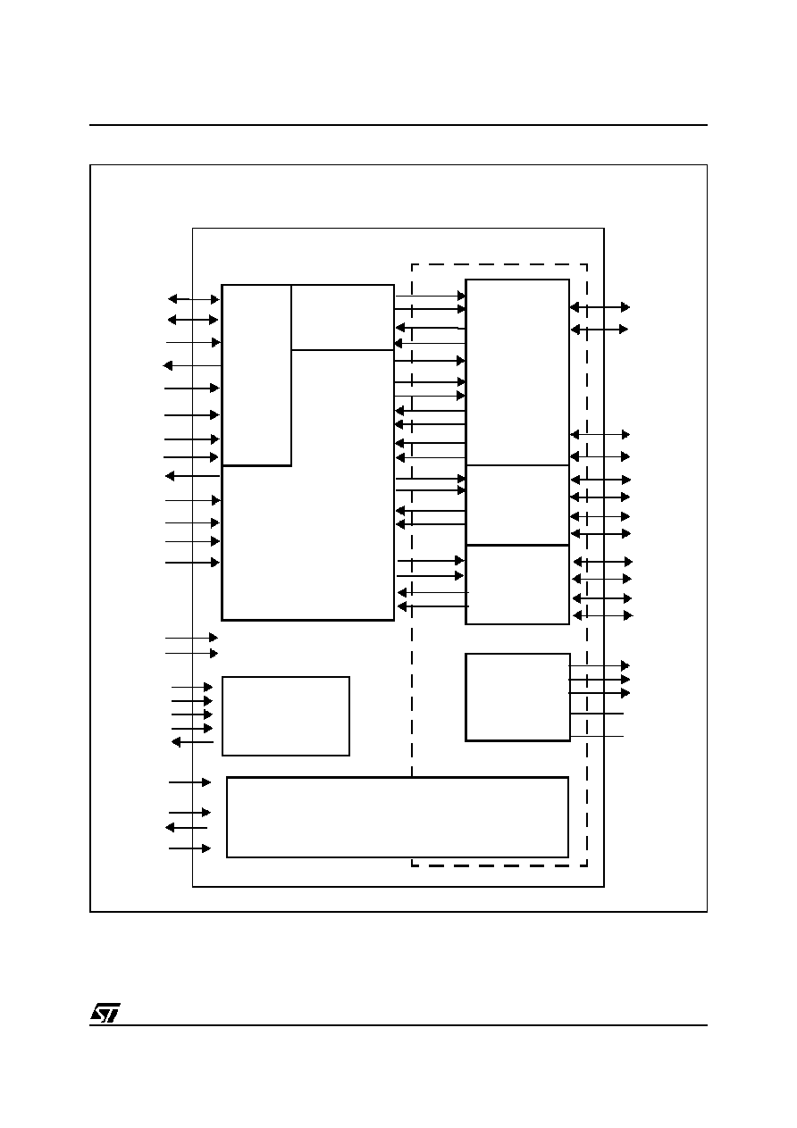
Figure 1.1 is a block diagram of the SBPH400-3. The portion of circuit which is circled by the
dash line is termed the
Cable Media Interface. All signals between the Digital Circuit and the
Cable Media Interface are pure digital signals. The signals which are driven on and received
from the cable are analog differential and common mode signals. The differential signals on
the cable transmit data or arbitration states, while common mode signals indicate the cable
connection status or transmission rate (speed).
2
SBPH400-3
5/43
Figure 1.1
SBP H400-3 block diagram
Strb_Tx
Strb_En
Data_Tx
Data_En
Speed_Tx
Strb_Rx
Data_Rx
Arb_A_Rx
Arb_B_Rx
Speed_Rx
Port_Status
Transmitter
&
Receiver
Port 1
Bias
D[0:7]
Ctl[0:1]
LReq
SClk
Cable Media Interface
(Driver/Receiver,
Arb. Comparator,
Port_Status,
Speed Monitor)
...
...
CPS
LPS
LKON
PC[0:2]
RESET#
TPA1
TPA1#
TPB1
TPB1#
TPBias1
TPA2
TPA2#
TPB2
TPB2#
R1
R0
Data
Decoder
LINK
Interface
I/O
Arbitration and
Control State Machine
Logic
ISO
Encoder/
TPBias2
TPBias3
Port 3
...
...
(same as Port 1)
TPA3
TPA3#
TPB3
TPB3#
CMC
JTAG
BUILT-IN
SELF TEST
TCK
TRST#
TMS
TDI
TDO
TEST
ACCESS
PORT
Port 2
(same as Port 1)
TESTENABLE
TESTMODE
LACT
PDISABLE
CLK24/QX0
SCO[2:0]
SCI[2:0]
QX1
2

6/43
SBPH400-3
2
Functional Description
2.1
Transmitter and receiver port interface
Figure 2.1
Analog port schematic
The SBPH400-3 implements three cable interface transceiver ports. Each port operates
independently from the other ports, under control of the device control logic. Each port
provides two pairs of signals, denoted TPA, TPA#, and TPB, TPB#. Each signal is
implemented using a driver and a receiver connected to a single pin (total of four pins per port).
In various modes, the driver and receiver are enabled, either separately or both at the same
time (for bi-directional signalling).
+
-
55
55
Strb_ Tx
Strb_ Ena ble
+
-
Da ta_Rx
+
+
-
-
+
-
7 k
5 5
5 5
+
-
+
+
-
-
+
-
Twisted Pair A
Twisted Pair B
VG
TPA
TPA*
TPB
TPB *
VG
T pB ia s '
0. 3
µ
f
m in
D riv e r
R ec eiv er
Arb_A_Rx
A rbitr ation
C o m pa ra to rs
S 20 0 _ref
S20 0
Da ta _T x
Da ta _Enab le
Strb _ Rx
A rb itra tion
C om p arator s
Arb _ B_Rx
Bia s
0.8V
C o m m o n m o d e sp ee d
s ig na l c u rren t
5 k
±
5 %
25 0 pF
(sh ared with TPA
a nd othe r p orts)
7 k
7 k
7k
T pB ia s de te c tion c o m pa rato r
I
CD
Ph ys ic al con ne c tio n
de te ction c o m pa rato r
Con
Tp Bia s d isa ble
+
-
S4 00 _r ef
S40 0
Spe e d_T x
S4 00
Sp ee d_T x
S20 0
Spe ed _Rx
Spe ed_ Rx
2

SBPH400-3
7/43
A port may be disconnected, disabled, suspended or active. When active, each port operates
in the following modes:
Idle mode: In this mode, each port's driver is disabled, i.e. the port presents a high impedance
on all four signals. The inputs are continuously sampled, and if a signal is detected (which will
normally indicate an arbitration signal from a connected port) then this is passed to the
arbitration logic.
Arbitration mode: In this mode, both pairs engage in bi-directional untimed digital signalling.
Each pair transmits (under the control of the arbitration logic) either a logic 1 using differential
signalling, a logic 0 using differential signalling, or high impedance Z. Simultaneously, the
signal on each pair is continuously sampled, and is interpreted as a logic 1, logic 0 or high
impedance Z. The sampled signal is a combination of the transmitted signal and the signal
being transmitted on the corresponding pair by a connected transceiver (NB the cable
implements a "twist" - TPA is connected to the far end TPB, and vice versa). The signal is
interpreted using the 1394 1's dominant rule and passed to the arbitration logic for
interpretation by the arbitration state machine. If a 11 level is received then this is interpreted
as a reset signal and passed to the control logic.
Speed signalling mode: Speed signalling uses common mode signalling. It is used to signal
the transmission speed capabilities of the device (during the Self_ID phase of bus initialization)
and in parallel with the transmission of Data_Prefix arbitration signal during arbitration to
indicate the speed of the packet about to be transmitted. To send a speed signal, the port
generates a common mode current signal on TPB and TPB# for 100 ns. This signal results in
a drop of the current mode bias voltage through a pair of 55 Ohm resistors connected between
the TpBias output and the TPA, TPA# pair at the receiving end. To receive a speed signal, the
port determines the speed by measuring the amount of voltage drop on the TPA pair,
compared to the TpBias signal it is generating. The port samples the speed signal at 20ns
intervals in order to provide filtering against intermediate values or against noise. The
SBPH400 requires two consecutive samples of a S200 or a S400 signal (as appropriate) in
order to identify a valid speed signal. If no speed signal is identified when data transmission
starts, then the data is assumed to be transmitted at S100 speed.
Data transmission mode: In this mode, which always follows arbitration mode, the port
transmits the data and strobe signals received from the data encoder on the TPB pair and the
TPA pair respectively. The transmission uses uni-directional differential data signalling on
each pair. Note that at the end of arbitration mode, the port will be transmitting an untimed
signal of 01. If the first bit to be transmitted is a zero, then this will cause a transition on "data"
(i.e. TPB, so that TPA, TPB transmit 00), if the first bit to be transmitted is a 1, then this will
cause a transition on "strobe" (i.e. TPA, so that TPA, TPB transmit 11). The receivers are
disabled during data transmission. At the end of data transmission mode, the port reverts to
idle mode.
Data reception mode: This mode always follows arbitration mode. The port presents high
impedance on its output drivers (and ignores the data which is being repeated to the other
ports by the data encoder/decoder). The port implements a differential receiver for each of
TPA (data) and TPB (strobe) pairs, and passes the received binary signals to the data
2

8/43
SBPH400-3
decoder. Advanced logic is used to ensure reception of the Data and Strobe signals at speeds
of up to 400 MHz.
2.2
Connect detect and bias
A low current connect detect circuit is used to detect a physical connection. A current, applied
to the TPA pair and sensed via a local Schmitt trigger, will indicate a disconnected state unless
there is a physical connection to ground via the 5K resistor connected to the TPB pair at the
far end. Note that this does not require the far end to be powered. This mechanism operates
only when the port is not generating TpBias.
In order to implement the cable detection, suspend/resume and speed signalling functions, a
common mode bias voltage has to be provided to the TPA pair. A separate TpBias pin is
provided for each port, which should be connected to the TPA pair via a pair of 55 Ohm
resistors, as shown in Figure 2.1. The use of a separate pin for each port avoids problems of
possible interference between the common mode signalling on each port, or possible mis-
detection of a disconnect.
A single external resistor should be provided between pins R0 and R1 in order to set the
internal operating and the cable driver output currents. A low TCR 3K
±
1% resistor should
be used.
2.3
Configuration pins
The SBPH400 provides six configuration pins which may be hard wired high or low, or may be
directly controlled from a link layer device. Four of the pins are used to initialize registers which
control configuration status bits in the self identification packet.
The PC[0:2] pins provide the power reset value for the power class register, which is reported
in the Self_ID packet in the pwr field.
The CMC pin provides the power reset value for the C register, with is reported in the Self_ID
packet in the C field to indicate if the node is a contender for the bus or isochronous resource
manager.
The LACT pin is used to initialize the value of the Link_active register on power reset. If set to
zero, this allows the node to appear as having an inactive link (the L field in the Self-ID packet
will be zero) until application software sets the Link_active bit to 1.
The PDISABLE pin is used to initialize all ports as disabled on power reset. This satisfies the
OHCI requirement, and allows software to be initialized before the device starts to participate
on power-on as a new device on the bus.
The ISO pin is used on power reset to determine the operating mode of the PHY/Link interface
(DC coupled or using a DC isolation barrier).
The SBPH400 also has a number of pins which are intended for use during production test
only, and are held to ground or V
DD
as appropriate in normal operation.
2

SBPH400-3
9/43
2.4
Suspend/Resume/Disable
Each port independently implements the P1394a suspend/resume proposal. At any one time,
a port may be disconnected, disabled, suspended or active.
On power reset, if PDISABLE = 0 then all ports are initialized as disconnected, and then, if any
ports are physically connected, the normal new connection actions taken. If PDISABLE = 1
then all ports are initialized as disabled.
When a port is not active, the TpBias output for the port is disabled, all outputs of the port are
set to high impedance and any incoming arbitration signals on TPA and TPB are ignored.
A port may be disabled or re-enabled by a command (register write) from the local link, or by
remote PHY command packet. While disabled, the port ignores any incoming TpBias signal
but the port continues to monitor its connection status using the connect_detect mechanism.
A change in connection status will cause an interrupt to the link or a LinkOn packet as
appropriate and according to the controlling flags. When re-enabled and connected, the port
is treated as suspended (see below).
When disconnected, a port ignores any incoming TpBias signal but continuously monitors the
connection status using the connect detect circuitry. On connection, the port attempts to
become active, but if an incoming TpBias is not then detected, then the port is suspended with
the fault bit set.
While active, the port continuously senses the common-mode bias input voltage on the TPB
pair. The presence of a bias voltage on the TPB pair indicates that the port is connected to an
active port on some other device. Similarly, the absence of a bias voltage indicates the lack of
such a connection or that the far end port has been powered off. On detection of loss of bias,
the port is treated as suspended (see below)
A port may be suspended by a remote PHY command packet. In this case, it engages in a
protocol with the remote connected port, resulting in that port too being suspended. It may be
suspended on loss of incoming TpBias on an active port. A port may also be suspended as a
result of its active connected port being suspended. A connected disabled port is treated as
suspended when re-enabled.
While suspended, the port monitors both TpBias and its connection state using the
connect_detect mechanism. If a disconnection is detected, then the port becomes
disconnected. If a TpBias signal is detected, then the port resumes to its active state. A port
may be instructed to resume by means of a remote command packet, in which case it
generates a TpBias signal. This will indicate to the connected peer port that it too should
resume.
It should be noted that any change of port state to or from the active state has the effect of a
topology change, and that reconfiguration of the bus is necessary. To ensure that this occurs,
the SBPH400 initiates the appropriate bus resets as defined in the P1394a proposal.
When a port becomes disconnected, disabled or suspended, it carries out the appropriate
actions and then automatically enters a low power mode. Normal operation (on full power) is
restored after an appropriate delay (to allow the internal clocks to stabilize) on any change in
2

10/43
SBPH400-3
port state. If all ports are in a low power state, and the PHY/Link interface is disabled, then the
SBPH400 implements the necessary delays to allow the SBPH400 core to enter a low power
state in future versions with no functional or timing change.
2.5
Data encoder/decoder
The data encoder/decoder implements the SGS-Thomson patented "Data/Strobe" clock
encoding technique, as described in the 1394 specification. Data to be transmitted is serialized
and encoded into the appropriate Data and Strobe signals. These are send simultaneously to
all active ports for outputting. All output is clocked by the SBPH400 clock derived from the local
crystal. Note that data to be transmitted may be received from an incoming port, or from the
link interface.
Data received from a port (only at most one port can be receiving data at any one time) is
resynchronized to the local clock using a small elastic buffer, as the clock frequency of the
incoming data may differ (by up to 200 ppm) from the local clock. The buffer is sized to avoid
underflow or overflow for the longest possible packet.The data is repeated to the ports and to
the link layer as described above, using the local reference clock.
2.6
Bus reset, arbitration and control
The SBPH400 enters bus reset on power reset, if the reset signal is sensed on any connected
port's arbitration signal lines, on a request from a link layer device, on resume from suspend
or on connection of detection on any port (possibly after a delay, to allow for an incoming
reset), on loss of TpBias on an active parent port, on entry to suspend as a result of the peer
port being suspended or disabled, or if the device stays in any state other than Idle, Tree-ID
start, Transmit or Receive for longer than 300
µ
sec. In some circumstances, the device will
arbitrate for the bus before generating a reset signal, as defined in the P1394a proposal. This
results in minimum disruption to high priority traffic.
On entry to reset, the arbitration control logic enters a Tree-ID phase. Either the node will be
identified an isolated node, or the node will be identified as the root, and all active ports will be
identified as child ports, or one active port will be the port to the node's parent, and the other
active ports will be identified as child ports.
The control logic will then engage in Self-ID, in which all nodes are allocated a node-ID and
exchange self-ID packets (see 2.7.2). All received self-ID packets are passed to the link layer
device. Speed capabilities are exchanged during the Self-ID process with all connected active
nodes.
In normal operation, the control logic implements the functions of the root, should the result of
the Tree-ID process be that this node becomes the root.
The control logic accepts arbitration requests from either the local link or any port. Upon receipt
of an arbitration request, the request is accepted locally (if the node is the root) or repeated
towards the root node via the parent port. Data Prefix (01) is transmitted on all other ports,
which indicates that any arbitration request from these ports is rejected.
2
SBPH400-3
11/43
If the request for transmit comes from the local link, then the arbitration control logic waits for
an appropriate gap (all interfaces Idle), and then (unless the request is an immediate request)
arbitrates as above.
The arbitration logic supports all the arbitration enhancements specified in IEEE P1394a:-
∑
arbitrated reset (a short reset which is delayed until a subaction gap arbitration)
∑
ack-accelerated arbitration (immediate arbitration after an ACK)
∑
fly-by arbitration (concatenation of packets after a packet received from a child
port)
2.7
PHY packets
2.7.1 Link device interaction
The SBPH400 will forward to the link (if the PHY/Link interface is active) every PHY packet
received on the bus.
The SBPH400 will interpret every PHY packet which it receives from the local link device for
transmission on the bus (in addition to responding to every PHY packet received from the bus).
The SBPH400 will act on it in exactly the same way as if the packet was received from the bus.
2.7.2 Self-ID packet
The Self-ID packet has the following format:
Figure 2.2
Self-ID packet format
1 0
phy_ID
0 L
gap_cnt
sp
c
pwr
p0
p1
p2
i
0
logical inverse of first quadlet
rsv
2
12/43
SBPH400-3
The fields in the Self-ID packet are derived as shown in Table 2.1.
2.7.3 Link_on packet
The SBPH400 will respond to a Link_on packet addressed to it received on the bus. The
packet has the following format:
Figure 2.3
Link_on packet format
If the logical AND of the LPS pin and the Link_active bit is zero, then the SBPH400 will
generate a 6.144 MHz signal on the LKON pin, until this logical value becomes 1. Otherwise
the packet is forwarded to the local link. Note that all Link_on packets received on the bus are
forwarded to the local link if it is active, whether or not the packets are addressed to the local
node.
2.7.4 PHY configuration packet
The SBPH400 will respond to every PHY configuration packet which it receives on the bus, or
from the link device for transmission on the bus. The packet has the format shown in Figure
2.4:
Table 2.1
Self ID packet fields
Field
Derived from
Comment
phy_ID
self-ID process or
set_PHY_ID packet
physical node identifier
L
Link enabled register
Logical AND of LPS signal and the Link_active register
gap_cnt
Gap_Count register
current value of Gap Count register
sp
Max_Phy_Speed
10b (S100, S200 and S400 capable)
rsv
(reserved)
00b
c
Contender register
current value of C register
pwr
Power class register
current value of Power class register
p0, p1 p2
port status for port 0, 1 and
2 respectively
01 - not active (disabled, disconnected or suspended)
10 - active and connected to parent node
11 - active and connected to child node
i
initiated reset
set whenever the node initiated the current bus reset
0 1
phy_ID
logical inverse of first quadlet
0000
0000
0000
0000
0000
0000
2

SBPH400-3
13/43
Figure 2.4
PHY configuration packet format
The fields in the PHY configuration packet are interpreted as shown in Table 2.2.
Note that either or both of R and T must be set to 1.
2.7.5 Ping packet
The SBPH400 supports the use of ping timing. The ping packet has the format shown in Figure
2.5:
Figure 2.5
Ping packet format
When the SBPH400 receives a ping packet from the bus or from the local link addressed to
the node, it responds immediately (without arbitration) with a Self_ID packet to both the bus
and the local link.
2.7.6 Remote Access and Reply
The SBPH supports remote access to its internal registers. On receipt of a remote access
packet addressed to the node (either from the bus or from the local link), the SBPH400 will
immediately respond with the appropriate remote reply packet. The remote access packet and
the reply packet are also forwarded to the local link.
Table 2.2
PHY configuration packet fields
Field
Definition
Comment
root_ID
physical ID
the physical node identifier of the node to become root on next reset
R
set root
The Force_Root bit in the SBPH400 is set if R=1 and root_ID = the
node_ID of this node
T
set gap count
If T=1, then the value of the gap count register in the SBPH400 is set
to gap_cnt.
gap_cnt
Gap_Count value
new value of Gap Count register
0 0
root_ID
logical inverse of first quadlet
R
0000
0000
0000
0000
T
gap_cnt
0 0
phy_ID
logical inverse of first quadlet
0
0000
0000
0000
0000
0
00
type (0)
2
14/43
SBPH400-3
Figure 2.6
Remote access packet format
Figure 2.7
Remote reply packet format
The fields in the remote access and remote reply packets are interpreted as shown in Table
2.3.
2.7.7 Remote Command and Confirmation packets
The SBPH400 responds to remote command packets by initiating the appropriate action and
immediately sending a remote confirmation packet.
Figure 2.8
Remote command packet format
Table 2.3
Remote Access and Remote Reply packet fields
Field
Comment
phy_ID
Physical node identifier of the destination of the packet (type = 1 or 5)
Physical node identifier of the source of the packet (type = 3 or 7)
type
1 - register read of the base registers
3 - register contents (base registers)
5 - register read of the paged registers
7 - register contents (paged registers)
page
0 - Port Status Page
1 - Product Identification Page
2-7 - (these pages not implemented, always responds with zero)
port
Identify the port for the selected register page. For values 0, 1 and 2, the page is as
defined in Table 2.17. For all other values the SBPH400 always responds with zero.
reg
If type = 1, then reg directly addresses one of the base registers.
If type = 5, then reg addresses 1000
2
+reg in the selected page and port.
data
Current value of the SBPH400 register addressed by the immediately preceding Remote
Access packet (reserved and unimplemented fields and registers are returned as zero).
0 0
phy_ID
logical inverse of first quadlet
0
port
reg
reserved
0
page
type
0 0
phy_ID
logical inverse of first quadlet
0
port
reg
data
0
page
type
0 0
phy_ID
logical inverse of first quadlet
0
port
0000
cmnd
0
000
type(8)
0000
2
SBPH400-3
15/43
Figure 2.9
Remote confirmation packet format
The fields in the remote command and remote confirmation packets are interpreted as shown
in Table 2.4.
2.8
Link interface
2.8.1 Overview
The link interface in the SBPH400 operates as described in the IEEE P1394a proposal.
The SBPH400 implements an interface to a single 1394 link layer device, using the pins D[0:7],
Ctl[0:1], LREQ, SClk, LPS and LKON. The interface is scalable, using 2 data bits in parallel
per 100 Mbit/sec. This enables the clock rate of the signals at this interface to remain at 50
MHz.
Table 2.4
Remote Command and Confirmation packet fields
Field
Comment
phy_ID
Physical node identifier of the destination of the packet (type = 8)
Physical node identifier of the source of the packet (type = A
16
)
type
8 - remote command packet
A
16
- remote confirmation packet
port
Identify the port for the command or confirmation. For values other than 0, 1 and 2, the
SBPH400 always responds with the OK bit set to zero in the confirmation packet.
f
current value of the Fault bit from SBPH400 register 1001
2
for the addressed port
c
current value of the Connected bit from SBPH400 register 1000
2
for the addressed port
b
current value of the Bias bit from SBPH400 register 1000
2
for the addressed port
d
current value of the Disabled bit from SBPH400 register 1000
2
for the addressed port
ok
1 if the immediately preceding remote command was accepted by the SBPH400, zero
otherwise
cmnd
type = 8:-
0 - NOP
1 - Transmit TX_DISABLE_NOTIFY then disable the port
2 - Initiate suspend
4 - Clear the port's Fault bit
5 - Enable port
6 - Resume port
type = A
16
:-
The cmnd value from the immediately preceding remote command packet
data
Current value of the SBPH400 register addressed by the immediately preceding Remote
Access packet (reserved and unimplemented fields and registers are returned as zero).
0 0
phy_ID
logical inverse of first quadlet
0
port
000
cmnd
0
000
type(A
16
)
f
c b d ok
2

16/43
SBPH400-3
The SBPH400 has control over the bidirectional pins. It will, upon request, transfer this control
to the link device, which can then drive these pins. The 8 bidirectional data pins D[0:7] form
the data bus. The portion of the D bus which carries packet data is left-justified starting with
the 0 bit. Packet data for 100 Mb/s transfers uses D[0:1], 200 Mb/s transfers use D[0:3], and
400 Mb/s transfers use D[0:7]. The unused D[n] signals are transmitted as `0' and are ignored
when the link device has control of the bus. The control bus CTL[0:1] carries the control
information. The LREQ pin is used by the link device to request access to the serial bus and
to read and write the chip registers.
2.8.2 Types of operation
The four basic operations which may occur at the PHY-Link interface are: request, status,
transmit and receive. Request is the only operation initiated by the link layer device. The link
layer device uses the request operation to read or write a register located in the SBPH400 or
to request the bus so that the SBPH400 can initiate a transmit action on the bus. The
SBPH400 initiates a receive action whenever a packet is received from the serial bus and a
status indication to notify events to the link layer device.
2.8.3 Control pins
When the SBPH400 has control of the PHY-Link interface the CTL[0:1] lines are encoded as
shown in Table 2.5.
When the link layer device has been granted the PHY-Link interface by the SBPH400, it should
encode the CTL[0:1] lines Table 2.6
Table 2.5
CTL[0:1] When the SBPH400 is driving
CTL[0:1]
NAME
DESCRIPTION
00
Idle
No activity (default mode)
01
Status
The SBPH400 is sending status information to the link device
10
Receive
An incoming packet is being transferred from the SBPH400 to the link
device
11
Grant
The link device is granted the bus to send a packet
Table 2.6
CTL[0:1] when the link is driving (upon grant from SBPH400)
NAME
DESCRIPTION
00
Idle
The link device has released the bus (normally after transmission).
Note that multiple Idles may need to be transmitted.
01
Hold
The link device is preparing data or wishes to reacquire the bus without
arbitrating to send another packet
10
Transmit
The link device is sending a packet to the SBPH400
11
unused
2
SBPH400-3
17/43
2.8.4 Link device request (LREQ)
The link layer device requests the bus or accesses a register in the SBPH400 by sending a
short serial stream on the LREQ pin. The information sent includes the type of bus request,
the speed at which the packet is to be sent, or a read or write command. The length of the
request stream depends on whether it is a bus request (8 bits), a read register request (9 bits),
a write register request (17 bits), or an accelerate control request (6 bits).
The request stream always commences with a start bit (value 1b) and terminates with a stop
bit (0b). Bit 0 is transmitted first on the serial request stream.
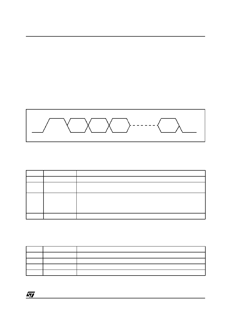
The LREQ timing and the definition of the bits in the transfer are shown in Figure 2.10
Figure 2.10
LREQ timing
The Bus Request is 8 bits long and is specified in Table 2.7. (Note that this is backwards
compatible with the 7-bit format as specified in IEEE 1394-1995, which is also supported by
the SBPH400.)
The Read Request is used to read a register in the device. It is 9 bits long and is specified in
Table 2.8.
Table 2.7
Bus request format
Bit(s)
Name
Description
0
Start_Bit
Indicates start of transfer. Always 1.
1-3
Request_Type
Indicates the type of bus request being performed. See Table 2.12 for the
encoding of this field.
4-6
Request_Speed
Indicates the speed at which the SBPH400 will be sending the packet for
this request. This field has the same encoding as the speed code from the
first symbol of the receive packet. See Table 2.11 for the encoding of this
field.
7
Stop_Bit
Indicates end of transfer. Always 0.
Table 2.8
Read register request format
Bit(s)
Name
Description
0
Start_Bit
Indicates the start of transfer. Always 1.
1-3
Request_Type
100b (Register read)
4-7
Address
Indicates the address of the physical register to be read.
8
Stop_Bit
Indicates end of transfer. Always 0.
LR0
LR1
LR2
LR3
LR(n-2)
LR(n-1)
2
18/43
SBPH400-3
The Write Request is used to write to a register in the device. It is 17 bits long and is specified
in Table 2.9.
The Accelerate Control Request is used to control the use of arbitration acceleration in order
to prevent Cycle Start packet starvation. It is 6 bits long and is specified in Table 2.10
The Request Speed field in the bus request is encoded as specified in Table 2.11:
Table 2.9
Write register request format
Bit(s)
Name
Description
0
Start_Bit
Indicates the start of transfer. Always 1.
1-3
Request_Type
101b (Register write)
4-7
Address
Indicates the address of the physical register to be written.
8-15
Data
Indicates the data to be written to the specified physical register.
16
Stop_Bit
Indicates end of transfer. Always 0.
Table 2.10
Accelerate control request format
Bit(s)
Name
Description
0
Start_Bit
Indicates the start of transfer. Always 1.
1-3
Request_Type
110b (AccCtrl)
4
Acceleration_Select
0 = Decelerate
1 = Accelerate
5
Stop_Bit
Indicates end of transfer. Always 0.
Table 2.11
Request speed field
LR[4:6]
Data Rate
000
S100
001
not supported (S1600)
010
S200
011
not supported (S3200)
100
S400
101
reserved
110
not supported (S800)
111
reserved
2

SBPH400-3
19/43
The Request Type field is encoded as specified in Table 2.10:
Table 2.12
Request type field
LR[1:3]
Name
Description
000
ImmReq
Used for Acknowledge Transfers. The SBPH400 takes control of the bus
immediately upon detecting idle without arbitration.
001
IsoReq
Used for Isochronous Transfers. The SBPH400 arbitrates after an
isochronous gap, or transmits immediately if an isochronous packet has
just been received from a child port (fly-by arbitration). The SBPH also
performs accelerated arbitrations (see AccCtrl below) after receiving this
request if the enab_accel register is set to 1.
010
PriReq
Used for Cycle Master requests. The SBPH400 arbitrates after a
subaction gap or, if acceleration enhancements are enabled (enab_accel
register is set to 1) and if accelerate control has been set to allow
accelerations (see AccCtrl below), arbitrates after an ACK packet has
been received, or transmits immediately if an ACK packet has just been
received on a child port (see Accelerate/Decelerate below), ignoring the
fair protocol. This is also used for the second and subsequent optimized
fair transfers
011
FairReq
Used for Fair Transfers. Used for Fair Transfers. The SBPH400 normally
arbitrates after subaction gap. If acceleration enhancements are enabled
(enab_accel register is set to 1) and if accelerate control has been set to
allow accelerations (see AccCtrl below), then the SBPH400 will arbitrate
after an ACK packet has been received, or transmit the packet
immediately if an ACK packet has been received on a child port. In all
cases the SBPH400 follows the fair protocol (one FairReq packet per
arbitration reset gap).
100
RdReg
Return specified register contents through a status transfer.
Note that the result is undefined if a previous RdReg request has not been
completed.
101
WrReg
Write to specified register.
110
AccCtrl
Accelerate control. The link should send an AccCtrl request with
Acceleration_Select = 0 (Decelerate) if it is not root and when its cycle
timer has counted a 125
µ
s interval. The SBPH400 will not employ ACK
accelerated arbitration or fly-by arbitration for asynchronous packets until
a subsequent Accelerate request with Acceleration_Select = 1
(Accelerate) is received or an IsoReq has been received. The link should
send an Accelerate request with Acceleration_Select = 1 after it has
received a cycle start packet if it has no isochronous packets to transmit
in the current isochronous cycle.
111
reserved
ignored
2

20/43
SBPH400-3
2.8.5 Bus request
The SBPH400 obeys the rules specified in the P1394a proposal for the disposition of requests
received from a link device, provided that the link device follows the P1394a rules for when it
may issue requests.
The link device sends the request for the bus for fair (FairReq) or priority (PriReq) access at
least one clock after the interface becomes idle or during a status transfer from the SBPH400.
A cycle master node uses a priority request (PriReq) to send the cycle start packet.
A receive state (CTL[0:1]=10) at any time during or after the link device sends a fair or priority
request transfer indicates to the link device that the request cannot yet been granted, due to
the arrival of an incoming packet. If arbitration acceleration is enabled, and the incoming
packet is null or has no more than 8 bits, then the SBPH400 retains the request, otherwise the
request is discarded as soon as the SBPH400 determines that the incoming packet has more
than 8 bits. The request always discarded if arbitration acceleration is not enabled. The link
device should reissue a discarded request on the next idle or status.
A link device uses the IsoReq request at any time to request the SBPH400 to send an
isochronous packet. The SBPH400 will wait for a an isochronous gap before arbitrating for the
bus. The SBPH400 will clear the request only when the bus has been won, or if it performs a
status transfer indicating a subaction gap (this indicates an error condition and should not
occur).
A link device must issue a ImmReq request to send an acknowledge packet during the
reception of a packet addressed to it or no later than the fourth SClk cycle after the interface
went idle. As soon as the packet reception ends the SBPH400 immediately takes control of
the bus and grants the bus to the link device. If the header CRC of the packet happens to be
bad the link device should release the bus immediately. Note that the link device should not
use this request to send another type of packet. This can be ensured by making the link device
wait for 160 ns after the end of the receive packet to allow the SBPH400 to grant it the bus for
the acknowledge. The bus is then released before starting another request.
After the link issues a request for the access to the bus (immediate, iso, fair, or priority) it
cannot issue another bus request until the SBPH400 indicates that the request is either "lost"
(incoming packet, other than an ACK packet when accelerations are enabled) or "won" (grant).
When a previous bus request is pending the SBPH400 ignores new bus requests.
All outstanding requests are cancelled on a bus reset.
2.8.6 Register Read/Write requests
For write requests, the SBPH400 takes the data field of the LREQ transfer and loads it into the
addressed register as soon as the transfer is complete.
For read requests, the SBPH400 returns the contents of the addressed register at the next
opportunity through a 16-bit status transfer. The link device may perform a read or write
register operation at any time.
2
SBPH400-3
21/43
2.8.7 Status transfer
A 4-bit status transfer of S[0:3] is initiated by the SBPH400 when any of the four status bits
S[0] to S[3] (as specified in Table 2.13) is set to 1. A 16-bit status transfer of s[0] to s[15] (as
specified in Table 2.13 is initiated by the link in response to a register read request from the
link device, or to indicate the node's new phy_ID after a bus reset during the Self_ID process.
After the link interface is idle, a status transfer is initiated with the assertion of status (CTL[0:1]
= 10) condition by the SBPH400. The first two bits of status information (S[0:1]) are made
available on D[0:1]. The status condition is held on CTL[0:1] for the duration of transfer. The
SBPH400 ensures that there is at least one clock cycle between status transfers.
Figure 2.11
Status transfer timing
Table 2.13
Status bits
Bit (S[n])
Name
Description
0
ArbitrationResetGap
This bit indicates that the SBPH400 has detected that the
serial bus has been idle for an arbitration reset gap time (this
is defined in the IEEE 1394 standard). This bit is used by the
link device in the busy/retry state machine. This bit is reset
after the status transfer or when a transfer occurs on the bus.
1
SubactionGap
This bit indicates that the SBPH400 has detected that the
serial bus has been idle for a subaction gap time (this is
defined in the IEEE 1394 standard). This bit is used by the link
device to detect the end of an isochronous cycle. This bit is
reset after a status transfer or when a transfer occurs on the
bus.
2
BusReset
This bit indicates that the SBPH400 has entered the bus reset
state. This bit is reset after a status transfer
3
PHY_Interrupt
This bit is set whenever any of the interrupt-generating status
bits (Loop detect, Power fail, State time-out, Port event) is set
to 1. This bit is reset after a status transfer.
4-7
Address
These bits indicate the address of the SBPH400 register
whose contents are being transferred to the link device
8-15
Data
These bits provide the current value of SBPH400's register.
00
01
01
01
00
00
S[0,1]
S[2,3]
S[14,15]
00
SBPH400
CTL[0:1]
SBPH400
D[0:1]
2

22/43
SBPH400-3
In the event of a packet reception during status transfer, the SBPH400 prematurely ends the
transfer by removing the status indication on the CTL[0:1]. Note that any status bits transferred
will be reset, even if the status transfer is prematurely terminated (i.e. if it is terminated after
the transfer of S[0:1], then S[0:1] will be reset. If it is terminated after the transfer of S[0:n]
where n>=3, then S[0:3] will be reset. The status transfer will be retried at the next available
opportunity if it was a 16 bit status transfer, or if it was a 4 bit status transfer and at least one
of the four status bits S[0] to S[3] is (still) 1.
2.8.8 Transmit
The link device requests access to the serial bus through LREQ when it wants to transmit
information. The SBPH400 arbitrates, using the timing algorithm appropriate to the request
type, to gain access to the serial bus. After the SBPH400 wins the arbitration, it grants the bus
to the link device by asserting grant on the CTL pins for one clock cycle, followed by idle for
one clock cycle. When it receives control of the bus, the link may assert one cycle of idle on
the CTL pins (this may be advisable when using PHY-Link isolation). While preparing data, the
link device keeps the ownership of the bus by asserting hold on the CTL pins. It is not
necessary for the link device to assert hold if it is ready to transmit as soon as bus is granted.
When it is ready to transmit a packet, the link device asserts transmit on the CTL pins along
with the first bits of the packet.
After sending the last bits of the packet when the link device does not wish to concatenate
another packet, the link device asserts idle on the CTL pins for two clock cycles before
tristating the CTL pins. After sending the last bits of the packet when the link device wishes to
concatenate another packet, the link device asserts hold on the CTL pins for one cycle,
together with the speed code for the next packet, followed by a single cycle of idle before
tristating the CTL pins. The link device may release the bus after the SBPH400 has asserted
grant by asserting idle on the CTL pins for three cycles, and may release the bus after
asserting hold by asserting idle on the CTL pins for two cycles.
The hold state indicates to the SBPH400 that the link device wants to send another packet
without releasing the bus (a concatenated packet). The SBPH400 responds to the hold by
waiting the required minimum time and then asserts transmit as before. The speed of the
concatenated packet is indicated at the time that the hold state is asserted, using the encoding
specified in Table 2.14.
Note that it is not permitted to transmit a S100 packet as a concatenated packet after
transmitting a higher speed packet. Note that, for compatibility with 1394-1995 PHYs, P1394a
requires that if "multi-speed concatenated packets" is not enabled (see Table 2.16), the speed
code for any concatenated packet which is received from the link will be ignored, and the
packet will be transmitted at the same speed as the packet to which it is concatenated. The
SBPH400 will supply the appropriate speed code as it transmits the packet on the bus.
When the link device has finished sending the last packet of the current bus ownership, it
releases the bus by asserting idle on the CTL pins for two consecutive clock cycles. The
transmit timing is shown in Figure 2.12.
2

SBPH400-3
23/43
Figure 2.12
Transmit timing
SBPH400
SBPH400
D[0:7]
SBPH400
SBPH400
00
11
00
ZZ
ZZ
ZZ
ZZ
ZZ
ZZ
ZZ
ZZ
ZZ
00
00
00
ZZ
ZZ
ZZ
ZZ
ZZ
ZZ
ZZ
ZZ
ZZ
ZZ
ZZ
ZZ
00
ZZ
00
01
10
10
10
00
00
ZZ
00
D0
D1
Dn
00
00
ZZ
ZZ
ZZ
ZZ
00
ZZ
ZZ
ZZ
00
Dn
00
ZZ
00
11
00
ZZ
ZZ
ZZ
ZZ
00
00
00
ZZ
ZZ
ZZ
ZZ
SP
ZZ
ZZ
ZZ
00
00
D0
D1
CTL[0:1]
D[0:7]
CTL[0:1]
D[0:7]
LINK DEVICE
CTL[0:1]
D[0:7]
LINK DEVICE
10
00
ZZ
01
ZZ
ZZ
ZZ
01
01
10
10
CTL[0:1]
LINK DEVICE
LINK DEVICE
ZZ
ZZ
00
01
Optional idle cycle
Single Packet
Concatenated packet
ZZ
ZZ
00
00
Optional idle cycle
2
24/43
SBPH400-3
2.8.9 Receive
When the SBPH400 detects the "data-on" state on the serial bus, it starts the receive operation
by asserting receive on the CTL pins and `1' on each of the D pins. The SBPH400 indicates
the beginning of the packet by placing on the D pins the speed code, as defined in Table 2.14.
The speed code is followed by the contents of the received packet using the appropriate range
of D pins (D[0:1] for S100, D[0:3] for S200 and D[0:7] for S400). The CTL pins will remain in
the receive state until the last symbol of the packet has been transferred to the link device. The
end of the packet is indicated by the CTL pins going back to the idle state. Note that the speed
code is part of the link interface protocol and is not included in the calculation of CRC. Note
that P1394a requires that, for compatibility with 1394-1995 PHYs, if "multi-speed
concatenated packets" is not enabled (see Table 2.16), any concatenated packet which is
received without a speed code is assumed to be transmitted at the same speed as the packet
to which it is concatenated. If the SBPH400 detects such a packet then it will indeed make this
assumption, and will supply the appropriate speed code in front of the packet as it transfers it
to the link device. The receive timing is shown in Figure 2.14.
Figure 2.13
Receive timing
Table 2.14
Speed codes on the LINK-PHY interface
D[0:7]
Data Rate
00000000
S100
01000000
S200
01010000
S400
11111111
"data-on" indication
00
10
10
10
10
10
10
00
00
00
FF
FF
SP
D0
D1
Dn
00
00
CTL[0:1]
D[0:7] (hex)
2

SBPH400-3
25/43
2.8.10 SBPH400 registers
The accessible SBPH400 registers are listed in Table 2.15. The descriptions of the fields are
given in Table 2.16.
Table 2.15
Accessible SBPH400 register
Address
0
1
2
3
4
5
6
7
0000
Physical_ID
R
PS
0001
RHB
IBR
Gap_count
0010
111b (Extended)
rsv
0011b (Total ports)
0011
Max speed
rsv
0000b (Delay)
0100
Link_active
C
000b (Jitter)
Power_class
0101
Resume_
int
ISBR
Loop
Pwr-fail
State
t_out
Port
event
Enab_
accel
Enab_
multi
0110
rsv
0111
Page_select
rsv
Port_select
1000-1111
Register 0-7 [Page_select]
Table 2.16
SBPH400 register fields
Field
Size
Type
Description
Physical_ID
6
R
The address of the node determined during self-identification.
R
1
R
When set to 1, indicates that the node is the root.
PS
1
R
Cable power status. This value always reflects the filtered voltage
sensed on the CPS pin.
RHB
1
R/W
Root Hold-off bit. When set to 1, instructs the node to attempt to
become the root during the next Tree-ID process. Value on power
reset is 0.
IBR
1
R/W
Initiate Bus Reset bit. When set to 1, instructs the SBPH400 to initiate
a bus reset for 166
µ
sec immediately. Always reads as zero.
Gap_Count
6
R/W
Arbitration timer setting. Used to optimize gap times based on the
topology of the network.
Extended
3
R
Always reads as 111b to indicate use of the extended PHY register
map
Total_Ports
4
R
Always reads as 3
Max_Speed
3
R
010b (maximum speed is S400)
Delay
4
R
0000b (maximum repeater delay is 144 ns)
Link_active
1
R/W
Set or cleared by software. Note that the value of the L bit transmitted
in the self-ID packet is the AND of the Link_active bit and the LPS pin.
Initialized to the value of the LACT configuration pin on power reset.
C
1
R/W
Contender. Set or cleared by software to control the value of the C bit
transmitted in the self-ID packet. On power reset this is initialized to
the value of the CMC pin.
Jitter
3
R
000b (fastest and slowest repeater delay differ by 20ns)
2

26/43
SBPH400-3
Power_class
3
R/W
Power class. Set by software to control the value of the pwr field
transmitted in the self-ID packet. On power reset, this is initialized to
the values of the PC[0:2] pins.
Resume_int
1
R/W
Resume interrupt enable. When set to 1, the SBPH400 sets
Port_event to 1 if resume operations commence for any port.
Initialized to 0 on power reset.
ISBR
1
R/W
Initiate short (arbitrated) bus reset. Unless entry to suspend or resume
is in progress for any of the SBPH400's ports, a write of one to this bit
requests the SBPH400 to arbitrate after a sub-action gap and issue a
short bus reset. Any outstanding fair request is abandoned. Unlike fair
bus requests, the request persists until won, or until a time-out forces
a long bus reset. Always reads as 0.
Loop
1
R/W
Loop detect interrupt. Set to one when the Tree-ID process detected
a loop. The PHY_interrupt status bit is set when this bit transitions
from 0 to 1. A register write with the value 1 in the field corresponding
to this bit clears the register to zero. A register write with a value 0 to
the field corresponding to this bit is ignored.
Pwr_fail
1
R/W
Cable power fail interrupt. Set when the PS register changes from 1 to
0. The PHY_interrupt status bit is set when this bit transitions from 0
to 1. A register write with the value 1 in the field corresponding to this
bit clears the register to zero. A register write with a value 0 to the field
corresponding to this bit is ignored.
State t_out
1
R/W
State time-out interrupt. Set to 1 when the arbitration state machine
has been in any state other than Idle, Tree-ID state T0, Transmit or
Receive for longer than 300
µ
sec. The PHY_interrupt status bit is set
when this bit transitions from 0 to 1. A register write with the value 1 in
the field corresponding to this bit clears the register to zero. A register
write with a value 0 to the field corresponding to this bit is ignored.
Port_event
1
R/W
Port event detect. Set to 1 when any of Connected, Bias, Disabled or
Fault change for a port whose Int_enable bit is one, or when resume
operations commence for any port and Resume_int is set to 1. The
PHY_interrupt status bit is set when this bit transitions from 0 to 1. A
register write with the value 1 in the field corresponding to this bit
clears the register to zero. A register write with a value 0 to the field
corresponding to this bit is ignored.
Enab_accel
1
R/W
Enable ACK accelerated and fly-by arbitration. Initialized to 0 on
power reset.
Enab_multi
1
R/W
Enable multi-speed packet concatenation. Initialized to 0 on power-on
reset.
Table 2.16
SBPH400 register fields (continued)
Field
Size
Type
Description
2
SBPH400-3
27/43
Page_select
3
R/W
Select extended register page for a subsequent PHY register read or
write operation.
0 = Port Status Page
1 = Product Identification Page
Initialized to 0 on power reset.
Port_select
4
R/W
Identify the port for the selected register page for a subsequent PHY
register read or write operation. For values 0, 1 and 2, the page is as
defined in Table 2.17. For all other values, a subsequent write to any
register in the page has no effect, and a subsequent read from any
register in the page returns zero. Initialized to 0 on power reset.
rsv
R/W
Field reserved in P1394a for future use. No effect on write, always
reads as zero.
Table 2.17
Port status page
Address
0
1
2
3
4
5
6
7
1000
AStat
BStat
Child
Con
Bias
Dis
1001
Negotiated_speed
Int_
enable
Fault
rsv
1010-1111
rsv
Table 2.18
Port status register fields
Field
Size
Type
Description
AStat
2
R
TPA line state on the selected port
(11
2
= Z, 01
2
= 1,10
2
= 0, 00
2
= invalid).
BStat
2
R
TPB line state on the selected port
(11
2
= Z, 01
2
= 1,10
2
= 0, 00
2
= invalid).
Child
1
R
If 1 the corresponding port is a child, else parent (only
valid after Self_ID)
Con
1
R
If 1 the corresponding port is connected, 0 if the port is
disconnected.
Bias
1
R
Reflects the Bias detected status on the port (1 = Bias
detected) after filtering
Dis
1
R/W
The port is disabled when this bit is set to 1, and
enabled when this bit is set to 0. Initialized to the value
of the PDISABLE pin on power reset.
Negotiated_speed
3
R
The negotiated speed for this port (only valid after
Self_ID). Possible values are 000b (S100), 001b
(S200), 010b (S400)
Table 2.16
SBPH400 register fields (continued)
Field
Size
Type
Description
2
28/43
SBPH400-3
The 6-bit Division field identifies the product group within SGS-THOMSON.
The 10 bit Product field identifies the product within the Division.
The Major revision will increment with each major revision of the device. The minor revision
will start at 0 for each major revision and will increment with mask fixes, etc.
Note:
The Division and Product fields are identical to the corresponding fields when accessing the
SBPH400 via the JTAG Test Access Port.
2.9
Reset and initialization
2.9.1 Power on
Figure 2.14
SBPH400 reset timing
Table 2.19
Product identification page
Address
0
1
2
3
4
5
6
7
1000
1 (Compliance level = P1394a)
1001
rsv
1010
Manufacturer's OUI (MSB - 00
16
)
0
0
0
0
0
0
0
0
1011
Manufacturer's OUI (80
16
)
1
0
0
0
0
0
0
0
1100
Manufacturer's OUI (LSB - E1
16
)
1
1
1
0
0
0
0
1
1101
Division (08
16
)
Prod-MSB (0)
0
0
1
0
0
0
0
0
1110
Product- LSB (01
16
)
0
0
0
0
0
0
0
1
1111
Major revision (1)
Minor revision (see note)
0
0
0
1
X
X
X
X
E x t os c illa to r
( w h e re u se d )
R e se t#
S B P H 4 0 0 o p e ra tio n a l
50 0
µ
s ec
1 0 0 n s m in
(V
D D
p re se n t)
2
SBPH400-3
29/43
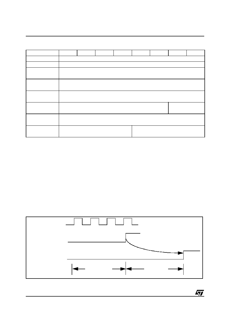
On Power on, the Reset# pin should be held low for 2ms to allow supplies to settle. To reset
the device when V
DD
is already present, the Reset# pin should be held low until a minimum of
100ns after the external oscillator (if used) is started and operating within specification. The
SBPH400 will wait for approximately 500
µ
sec to allow its internal clocking circuitry to stabilize.
At the end of the nominal 500
µ
sec period, the SBPH400 becomes fully operational. Prior to
the SBPH400 becoming fully operational, all outputs on the PHY/Link interface are held in high
impedance, as are the TpBias and TPA and TPB pins for all three ports. When the SBPH400
becomes fully operational, it senses the ISO, PC[0:2], CMC, LACT and PDISABLE. If ISO = 0,
then all outputs on the PHY/Link interface are taken to zero, and the SBPH400 will also then
respond to LPS if this pin is active (see 2.9.2).
2.9.2 PHY/Link Interface start-up
The PHY/Link interface is controlled by the link device via the LPS signal. In order to indicate
to the SBPH400 that the link interface is active, LPS should either be held to a logic 1 (possibly
by connecting to the V
D D
supplying the link layer device) or be connected to a pulsed output
which meets the specification shown in Figure 2.15 and Table 2.20. If neither of these is true
after power reset (see above), then no signal is considered to be received on LPS, the link
interface continues to be disabled, and the SBPH400 operates as a PHY repeater.
Figure 2.15
LPS timing (isolated interface)
When LPS is asserted, the PHY/Link interface starts as illustrated in Figure 2.16
Table 2.20
LPS timings
Symbol
Parameter
Unit
Min
Typ
Max
T
LPSL
LPS low time (isolated interface)
ns
90
1000
T
LPSH
LPS high time (Isolated interface)
ns
90
1000
T
LPSH
T
LPSL
LPS
(isolated)
2
30/43
SBPH400-3
Figure 2.16
PHY/Link interface start-up timing
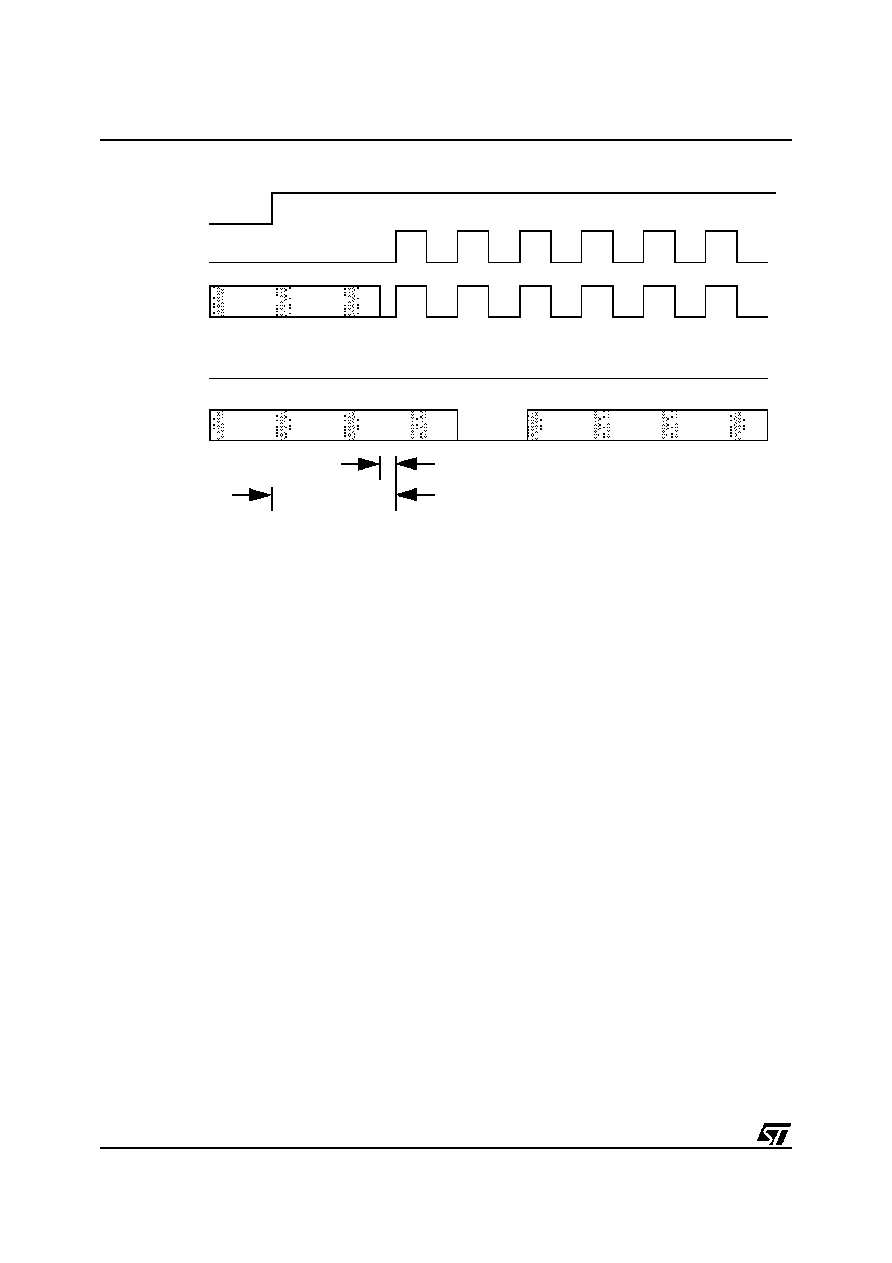
When LPS is reasserted, the SBPH400 resumes sending SCLK (if necessary) after 40-60 ns
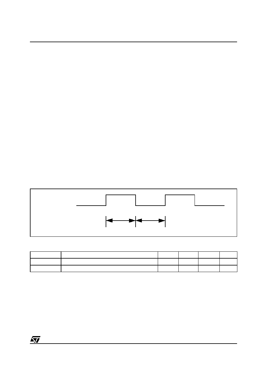
if the SBPH400 is operational, or otherwise after a nominal period of 500
µ
sec if LPS is used
to bring the SBPH400 out of suspend. If the interface is operating in direct mode (ISO = 0) then
Ctl[0:1] and D[0:7] are held zero. If the interface is operating in isolated mode (ISO = 1), then
the SBPH400 maintains high impedance for the first cycle of SCLK, asserts zeros on Ctl[0:1]
and D[0:7] for the second cycle of the resumed SCLK, and maintains high impedance for
cycles 3 to 7. The SBPH400 asserts a nominal receive indication on Ctl[0:1] for the eigth cycle,
while simultaneously indicating data_prefix on D[0:7] (all 1's). This is maintained for further
cycles if the SBPH400 is in a state where it would otherwise be transferring data.
2.9.3 PHY/Link interface reset and disable
The PHY-Link interface may be reset by taking LPS low for a minimum of 2.75
µ
sec, but less
than 25
µ
sec. During this time the Ctl[0:1] and D[0:7] signals are disabled, but the SBPH400
continues to provide SCLK.
If neither of these is true for a period greater than 25
µ
sec, then no signal is considered to be
received on LPS, the link interface is disabled, and the SBPH400 operates as a PHY repeater.
When the link interface is disabled, all outputs are held to zero if the interface is operating in
direct mode (ISO = 0), otherwise (ISO = 1) all outputs are maintained in high impedance. The
LP S
S C lk (d ir e ct)
S C lk (is o)
C [0 :1 ], D[0:7 ]
C [0 :1 ], D[0:7 ]
(iso )
(dire ct)
5 n s (m in)
40 - 6 0 n s (S BP H 400 op era tio na l)
50 0
µ
s n om ina l (S B P H 40 0 susp e nde d)
2

SBPH400-3
31/43
timing parameters are given in Table 2.21, and the signal relationships are illustrated in Figure
2.17 and Figure 2.18.
Figure 2.17
PHY-Link reset timing
Figure 2.18
PHY-Link disable timing
Table 2.21
PHY/Link interface reset and disable timing parameters
Symbol
Parameter
Unit
Min
Typ
Max
T
LPS_RESET
Time for SBPH400 to recognize LPS logically
deasserted and reset the interface
µ
s
1.2
2.75
T
LPS_DIS
Time for SBPH400 to recognize LPS logically
deasserted and disable the interface
µ
s
25
30
T
RESTORE
Time to permit the optional differentiator and
isolation circuits to restore during an interface
reset
µ
s
15
20
SCLK
LPS
LPS
(isolated)
CTL
DATA
LREQ
T
LPS_RESET
T
RESTORE
SCLK
LPS
LPS
(isolated)
CTL
DATA
LREQ
T
LPS_DISABLE
T
RESTORE
2

32/43
SBPH400-3
2.9.4 LKON (link on)
The LKON pin is used as an output to indicate that the SBPH400 has received a Link_On
packet. If the there is no signal on the LPS pin (indicating that the link device is not currently
powered) or the Link_active register is zero (link interface turned off by software) and a
Link_On packet is received addressed to the node, then a 6.144 MHz signal is output on the
LKON pin. This signal is turned off within 500 ns when both there is a signal received on LPS
and the Link_active register is 1.
2.10 ISO (isolation)
The SBPH400 supports the use of an isolation barrier between the chip and a link device. If
ISO is set high, then the an internal pulsed differentiating function is used on the CTL[0:1] and
the D[0:7] pins when used as outputs. Appropriate threshold circuitry is included on these pins
when used as inputs to interpret differentiated signals correctly. The differentiation circuitry
transmits a 1 or a 0 when there is a logical transition to 1 or 0 respectively, otherwise the output
is set to high impedance. This is shown in Table 2.22. This allows an arbitrary sequence of 1's
or 0's to be transmitted across an AC coupled isolation interface.
2.11 CPS (cable power status)
This input should be connected to the power supply provided from the cable via an external
series 400 KOhm resistor. The internal logic associated with this pin provides a nominal filtered
cable power fail voltage (as applied to the external resistor) threshold of 6.25 volts. The internal
logic will report 1 in the PS register when the external voltage on the resistor exceeds the
threshold, and will report 0 in the PS register when the external voltage falls below the
threshold. A transition from 1 to 0 on the value in the PS register causes the Pwr_fail register
to be set to 1, which in turn will cause a link status transfer with the PHY_Interrupt bit set if the
Link interface is active, otherwise will cause a LinkOn signal. Appropriate protection is
incorporated in the SBPH400 for cable power voltages within the 1394 specification applied
via the external series resistor.
Table 2.22
Output differentiation for isolation
Next
0
1
Previous
0
Z
1
1
0
Z
2

SBPH400-3
33/43
3
Pin Description
Table 3.1
Pin description - normal operation
Pin name
Pin number
I/O
Description
AGND
15, 23, 25, 80
Analog Ground
AVDD
6, 24, 26, 79
Analog Supply Voltage
CLK24
38
I
External 24.576 MHz oscillator input (optional, see QX0)
CMC
64
I
Configuration Manager Contender. Used to initialize the C register
at power-on reset. It should be programmed by connecting it to
V
DD
(C=1) or GND (C=0).
CPS
78
I
Cable power status.
CTL[0:1]
46, 45
I/O
Control signals for PHY-Link interface
D[0:7]
59 - 51
I/O
Data signals for PHY-Link interface
DGND
12, 13, 14, 27,
28, 29, 30, 31,
34, 40, 43, 48,
49, 50, 61, 69,
70, 72, 73, 74
Digital Ground
DVDD
32, 33, 47, 71
Digital Supply Voltage
ISO
68
I
Link interface isolation logic control. Logic level 1 on this pin
enables the isolation logic, 0 disables the isolation logic (normally
tied to V
DD
or GND as required)
LACT
41
I
Link Active. Used to initialize the Link Active register on power
reset. It should be programmed by connecting it to V
DD
(Link Active
= 1) or GND (Link Active = 0).
LKON
42
O
Link on o/p
LPS
62
I
Link power status.
LREQ
44
I
Link request to SBPH400
N/C
35, 75, 76
I
Inputs not used in normal operation, may be connected to V
DD
or
GND, or left unconnected.
OGND
37
I
Oscillator ground
OVDD
39
I
Oscillator supply voltage
PC[0:2]
65 - 67
I
Power Class input
PDISABLE
63
I
Ports disable. Used to initialize all three ports as disabled on
power-on reset.
QX0
38
I
24.508 MHz crystal input 0 (optional, see CLK24)
QX1
36
I
24.508 MHz crystal input 1 (optional, left unconnected if not used,
must not be taken to power or GND)
R[0:1]
22, 21
External resistor for bias current setting
RESET#
77
I
Reset. Taking this signal low causes all activity to cease. When this
signal is taken high, all appropriate registers and outputs are
initialized to their power reset values and a 166
µ
sec bus reset is
initiated.
2

34/43
SBPH400-3
Some pins on the SBPH400 have different functionality in various test modes. Table 3.2
identifies these pins for ease of reference, but the full description of the associate functions is
not included in this data sheet.
SCLK
60
O
Clock to Link device - 49.152 MHz
TPA1
1
I/O
Positive signal of cable pair A of port 1
TPA1#
2
I/O
Negative signal of cable pair A of port 1
TPB1
3
I/O
Positive signal of cable pair B of port 1
TPB1#
4
I/O
Negative signal of cable pair B of port 1
TPA2
7
I/O
Positive signal of cable pair A of port 2
TPA2#
8
I/O
Negative signal of cable pair A of port 2
TPB2
9
I/O
Positive signal of cable pair B of port 2
TPB2#
10
I/O
Negative signal of cable pair B of port 2
TPA3
16
I/O
Positive signal of cable pair A of port 3
TPA3#
17
I/O
Negative signal of cable pair A of port 3
TPB3
18
I/O
Positive signal of cable pair B of port 3
TPB3#
19
I/O
Negative signal of cable pair B of port 3
TPBIAS1
5
O
Cable Termination voltage source for port 1
TPBIAS2
11
O
Cable Termination voltage source for port 2
TPBIAS3
20
O
Cable Termination voltage source for port 3
Table 3.2
Pin description - test pins
Pin name
Pin number
I/O
Description
CLK98
35
I
98.304 MHz Oscillator input, used when PLLDIS is tied to V
DD
PLLDIS
49
I
Internal PLL disable pin. Tie to V
DD
to disable internal PLL.
SCI[0:2]
76, 67, 65
I
Used to serially shift data into the SBPH400 for production test
SCO[0:2]
68, 66, 64
I
Used to serially shift data out of the SBPH400 for production test
TCK
72
I
Test clock. Used to clock data into and out of the SBPH400 during
operation of the Test Access Port or production test.
TDI
75
I
Test Data Input. Used to serially shift test data and test instructions
into the SBPH400 during TAP operations.
TDO
63
O
Test Data Output. Used to serially shift test data and test
instructions out of the SBPH400 during TAP operations.
TEST
ENABLE
70
I
Reserved for production test
TESTMODE
30
I
Reserved for production test
TMS
69
I
Test Mode Select. This signal controls the state of the TAP
controller within the SBPH400.
TRST#
40
I
Test Reset. Resets the TAP controller.
Table 3.1
Pin description - normal operation (continued)
Pin name
Pin number
I/O
Description
SBPH400-3
35/43
4
Electrical Specifications
4.1
Absolute maximum ratings
Note:
Stresses greater those listed under "Absolute Maximum Ratings" may cause permanent dam-
age to the device. This is a stress rating only and functional operation of the device at these
or any other conditions above those indicated in the operational sections of this specification
is not guaranteed. Exposure to absolute maximum rating conditions for extended periods may
affect device reliability. During overload conditions (
V
IN
>
V
DD
or
V
IN
<
V
SS
) the voltage on pins
with respect to ground (
V
SS
) must not exceed the values defined by the Absolute Maximum
Ratings.
4.2
Operating conditions
Table 4.1
Absolute maximunm ratings
Symbol
Parameter
Units
Min
Max
V
DD
Supply Voltage
V
0
4
V
INL
Logic signal input low level
V
-0.5
V
INH
Serial signal input level
TTL input signals
V
V
V
DD
+0.5
5.5
T
∞
C
MAX
Maximum assembly temperature (for 10
seconds maximum)
Storage temperature
∞
C
∞
C
-65
260
150
Table 4.2
Operating conditions
Symbol
Parameter
Units
Min
Typ
Max
V
DD
Supply Voltage
V
3.0
3.3
3.6
Supply Ripple (DC to 1 GHz)
mV
100
T
A
Ambient temperature
∞
C
0
27
70
I
DD
Supply current @ 25
∞
C, 3.3 volts
with parallel outputs loaded by 10pF
mA
300
36/43
SBPH400-3
4.3
DC characteristics
The following values apply to the analog signals TPAn, TPAn#
The following values apply to the analog signals TPBn, TPBn#
Table 4.3
DC characteristics for TPAn, TPAn#
Symbol
Parameter
Units
Min
Typ
Max
V
OD
Differential output peak-to-peak voltage,
terminated by 55
load
mV
172
265
V
(OFF)
Off-state common mode output voltage
mV
20
Z
IC
Common mode impedance (driver disabled)
k
pF
20
24
Z
ID
Differential impedance (driver disabled)
k
pF
6
6
V
ARB1
Serial input differential amplitude for arbitration '1'
detect
mV
168
V
ARBZ
Serial input differential amplitude for arbitration 'Z'
detect
mV
-89
89
V
ARB0
Serial input differential amplitude for arbitration '0'
detect
mV
-168
V
ISWS
Serial input differential amplitude (absolute value)
during data transmission
mV
118
-
260
V
IT200
Speed signal threshold voltage relative to TPBIAS
(TPBIAS-TPA common mode voltage), S200
mV
139
264
V
IT400
Speed signalling threshold voltage relative to
TPBIAS (TPBIAS-TPA common mode voltage),
S400
mV
445
682
Table 4.4
DC characteristics for TPBn, TPBn#
Symbol
Parameter
Units
Min
Typ
Max
V
OD
Differential output peak-to-peak voltage, terminated by
55
load
mV
172
265
V
(OFF)
Off-state common mode output voltage
mV
20
Z
IC
Common mode impedance (driver disabled)
k
pF
20
24
V
TH_BIAS_CON
TpBias connect threshold
V
1.0
V
TH_BIAS_DIS
TpBias disconnect threshold
V
0.6
I
CM100
Common mode output current, speed signalling off or
speed signal = S100
mA
-0.81
0.44
I
CM200
Common mode output current, speed signal = S200
mA
-2.53
-4.84
I
CM400
Common mode output current, speed signal = S400
mA
-8.10
-12.4
V
ARB1
Serial input differential amplitude for arbitration '1'
detect
mV
168
V
ARBZ
Serial input differential amplitude for arbitration 'Z'
detect
mV
-89
89
SBPH400-3
37/43
The following values apply to the appropriate device pins in each case
V
ARB0
Serial input differential amplitude for arbitration '0'
detect
mV
-168
V
ISWS
Serial input differential amplitude (absolute value)
during data transmission
mV
118
-
260
Table 4.5
DC characteristics
Symbol
Parameter
Units
Min
Typ
Max
V
OH
High level output voltage (I
OH
= -4 mA)
V
2.8
V
OHD
High level output voltage (I
OH
= -9 mA, CTL[0:1],
D[0:7], SCLK and LKON outputs)
V
V
DD
-0.4
V
OL
Low level output voltage (I
OL
= 4 mA)
V
0.4
V
OLD
Low level output voltage (I
OL
= 9 mA, CTL[0:1],
D[0:7], SCLK and LKON outputs)
V
0.4
V
IH
High level input voltage
V
2.6
V
IL
Low level input voltage
V
0.7
I
I
Input current for CMC, LREQ, LPS, PC[0:2],
RESET#, ISO, PWRDWN, EXTCLK inputs
µ
A
-10.0
+10.0
I
PU
Input current for TDI, TMS, TRST# inputs
µ
A
-125
- 25
I
PD
Input current for TESTMODE, BISTRUN, TCK
inputs
µ
A
+25
+125
I
OZ
OFF-state output current, CTL[0:1], D[0:7], LKON,
TDO
mA
-10.0
+10.0
V
LIT_ISO+
Positive input threshold voltage on LPS input
(V
DD
=3.3V)
V
1.8
V
LIT_ISO-
Negative input threshold voltage on LPS input
(V
DD
=3.3V)
V
1.0
V
IT_ISO+
Positive input thresholds voltage, CTL[0:1], D[0:7],
LREQ inputs
V
V
DD
/2
+0.3
V
DD
/2
+0.8
V
IT_ISO-
Negative input thresholds voltage, CTL[0:1],
D[0:7], LREQ inputs
V
V
DD
/2
-0.8
V
DD
/2
-0.3
V
CPS
Threshold input voltage on CPS input as applied
via an external 400 K Ohm resistor
V
5.0
6.25
7.5
V
O
TPBIAS output voltage
V
1.665
1.85
2.015
Table 4.4
DC characteristics for TPBn, TPBn# (continued)
Symbol
Parameter
Units
Min
Typ
Max
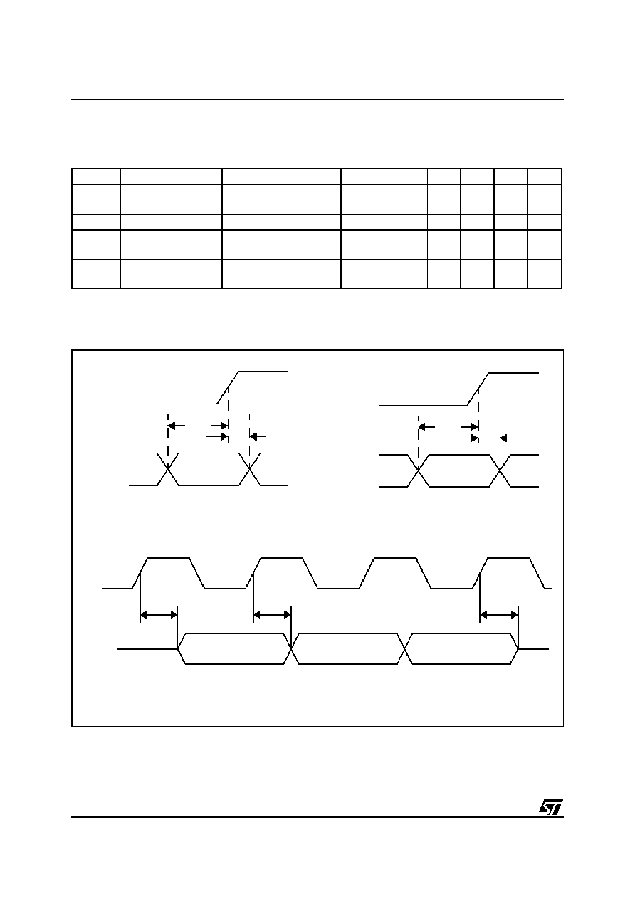
38/43
SBPH400-3
5
AC characteristics
Figure 5.1
Digital interface timing
Table 5.1
AC characteristics (analog interfaces)
Symbol
Parameter
Measured
Condition
Unit
Min
Typ
Max
Transmit jitter
(TPA, TPB)
ns
0.15
Transmit Skew
between TPA and TPB
ns
0.10
t
r
Transmit rise time
10% to 90%
Rl = 56
,
Cl = 10pF
ns
0.5
1.2
t
f
Transmit fall time
10% to 90%
Rl = 56
,
Cl = 10pF
ns
0.5
1.2
SCLK
D, CTL, LREQ
tpsu
tph
Link device to SBPH400 device timing
(NB SCLK runs from SBPH400 to link device)
SCLK
D, CTL
tlsu
tlh
SBPH400 to Link device timing
SCLK
CTL
DATA
LPS
t
d1
t
d2
t
d3
Link device to SBPH400 timing at the link
(Note: SCLK runs from the SBPH to the link device)
SBPH400-3
39/43
Table 5.2
AC characteristics (digital interfaces)
Symbol Parameter
Measured
Condition Unit
Min
Typ
Max
t
psu
D, CTL, LREQ input setup to SCLK
output
50% to 50%
ns
6
t
ph
D, CTL, LREQ hold from SCLK output 50% to 50%
ns
0
t
lsu
D, CTL output setup to SCLK
50% to 50%
ns
6.5
t
lh
D, CTL output hold from SCLK
50% to 50%
ns
0.5
t
d1
Delay time, SCLK input high to initial
instances of D, CTL and LREQ
outputs valid
50% to 50%
ns
1
10
t
d2
Delay time, SCLK input high to
subsequent instances of D, CTL and
LREQ outputs valid
50% to 50%
ns
1
10
t
d3
Delay time, SCLK input high to D, CTL
and LREQ outputs invalid (tri-state)
50% to 50%
ns
1
10
Table 5.3
Clock and reset parameters
Symbol Parameter
Measured
Condition Unit
Min
Typ
Max
Fextclk
External clock Frequency
24.576 MHz +/- 2.45 KHz
Dextclk
External clock duty cycle
50% to 50%
45%
55%
Jextclk
External clock Jitter peak to peak
100 pS peak to peak
F
SCLK
SCLK frequency
50% to 50%
Fextclk
◊
2
D
SCLK
SCLK duty cycle
50% to 50%
45%
55%
Power-on reset time, RESET# input
ms
2
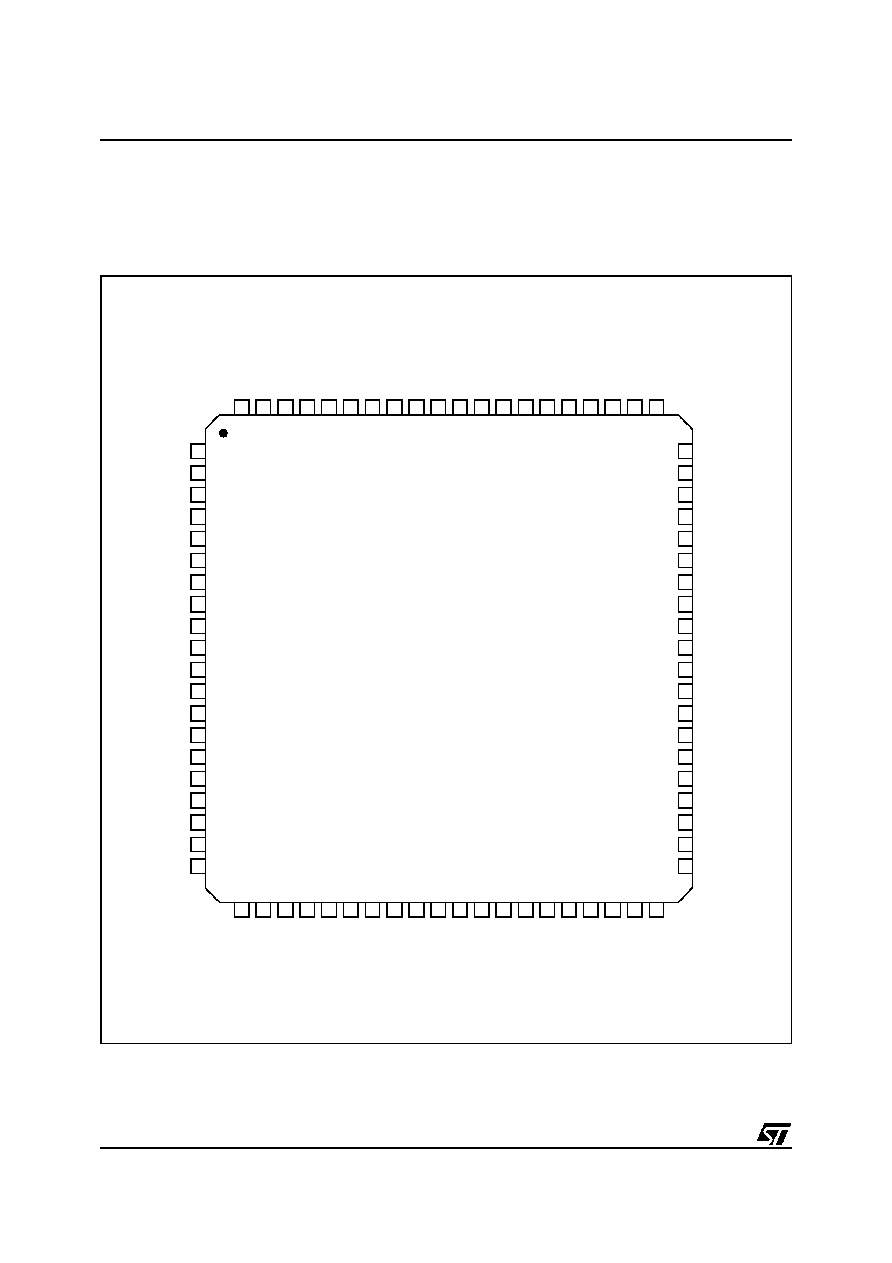
40/43
SBPH400-3
6
Package Specifications
The S B PH 4 00 -3 is available in a 80 pin plastic thin quad flat pack
Figure 6.1
Normal operation pinout for 80 pin 12mm x 12mmTQFP
1
2
3
4
5
6
7
8
9
10
11
12
13
14
15
16
17
18
19
20
25 26 27 28 29 30 31 32 33 34 35 36 37 38 39 40
41
42
43
44
45
46
47
48
49
50
51
52
53
54
55
59
60
56
57
58
80 79 78 77 76 75 74 73 72 71 70 69 68 67 66 65
TPBIAS1
AV
D D
TPA1
TPA1#
TPB1
TPB1#
TPA2
TPA2#
TPB2
TPB2#
TPA3
TPA3#
TPB3
R0
R1
AGN
D
AV
DD
QX0
/
C
L
K
2
4
OVD
D
DG
ND
LACT
CTL0
CTL1
DATA7
DATA6
DATA5
LKON
DGND
SCLK
LREQ
CMC
PC
1
DG
ND
LP
S
N/
C
R
E
SET
#
CP
S
AV
D
D
AG
N
D
SBPH400-3
12mm x 12mm
80 lead TQFP
21 22 2324
DG
ND
DV
DD
AGN
D
AVD
D
64 63 62 61
DG
ND
P
D
I
S
ABL
E
PC
0
TPB3#
DGND
PC
2
IS
O
DG
ND
DG
ND
DV
DD
DG
ND
DVDD
DGND
DGND
TPBIAS2
TPBIAS3
DGND
DGND
AGND
DG
ND
DG
ND
DG
ND
DG
ND
DV
DD
DGND
DATA4
DATA3
DATA2
DVDD
DATA1
DATA0
DG
ND
N/
C
DG
ND
N/
C
QX
1
OG
N
D

SBPH400-3
41/43
Figure 6.2
Data for 80 pin 12mm x 12mmTQFP
BODY + 2.00 mm FOOTPRINT
DIMS
TOLS/LEADS
64L
80L
A
MAX
1.60
A1
.05 MIN /.15 MAX
A2
+ .05
1.40
D
+ .20
14.00
D1
+ .10
12.00
E
+ .20
14.00
E1
+ .10
12.00
L
+1.5/-.10
.60
e
BASIC
.65
.50
b
+ .05
.30
.22
0
0
0
- 7
0
ddd
MAX
.13
.08
ccc
MAX
.10
.08
Body: 12 x 12 x 1.60 mm
A
A2
A1
B
C
16
17
32
33
48
49
64
E3
D3
E1
E
D1
D
e
1
K
B
TQFP64
L
L1
Seating Pl ane
0.10mm
D
D1
E
E1
A2
1.0 ref
N
1
e
b
A1
L
A
b

42/43
SBPH400-3
7
Application Circuit
Note:
Isolation components when using an isolated PHY-Link interface not shown;
1
2
3
4
5
6
7
8
9
1 0
1 1
1 2
1 3
1 4
1 5
1 6
1 7
1 8
19
20
2 5
26
27
28
2 9
3 0
3 1
32
33
34
35
36
3 7
3 8
39
40
41
42
43
44
45
46
47
48
49
50
51
52
53
54
55
59
60
56
57
58
8 0 79 7 8 77 7 6 75
7 4 73
7 2 71
70 69
68
67
66 65
TPBIAS1
AV DD
TPA1
TPA1#
TPB1
TPB1#
TPA2
TPA2#
TPB2
TPB2#
TPA3
TPA3
TPB3
R0
R1
AGND
AVDD
QX0/
C
L
K
2
4
OVDD
DGND
LA CT
CTL0
CTL1
D ATA 7
D ATA 6
D ATA 5
LK ON
D GN D
SCLK
LREQ
CM
C
PC
1
DGND
LP
S
N/
C
RE
S
E
T
#
CP
S
AVDD
AGND
SBPH400-3
21
22
2 3
2 4
DGND
DVDD
AGND
AVDD
64 6 3 62
61
DGND
PD
IS
A
B
L
E
PC
0
TPB3#
DG ND
PC
2
ISO
DGND
DGND
DVDD
DGND
D VD D
D GN D
D GN D
TPBIAS 2
TPBIAS 3
DG ND
DGND
AGND
DGND
DGND
DGND
DGND
DVDD
D GN D
D ATA 4
D ATA 3
D ATA 2
D VD D
D ATA 1
D ATA 0
DGND
N/
C
DGND
N/
C
QX1
OGND
3 00nF - 1
µ
F
V
D D
55
55
55
55
5 K
250 pF
Ca ble
C able
G ro und
V
D D
0. 1
µ
F
V
D D
10 0K
V
D D
u ser setting s
V
D D
V
D D
V
D D
V
D D
3.0K
+/- 1 %
F or TP A 2/A2 *, TP B2 /B 2*, T P B I A S 2,
T P A 3 /A 3* , TP B 3/B 3* a nd T P B I A S 3
c om po nent con ne cti o ns ar e the sam e as
T P A 1/A 1 *, TP B1 /B 1* and TP B IA S 1
.
L
I
N
K
I
N
TERF
A
C
E
(
*
)
(* ) Iso lation cir cu it use d if I S O pin enab le
40 0K
E xternal 24 .576 M H z Cr ystal O R E xternal os cill ator o ption
N /C
N C* *
N /C
N /C
V
D D
Ca ble P o w er
(* *) A ll N /C ( no n connec ted ) p ins, B UT N O T N C ** ( p in 3 6) may b e con nec ted to e it her G N D o r V
D D

43/43
Notes
Information furnished is believed to be accurate and reliable. However, SGS-THOMSON Microelectronics assumes no
responsibility for the consequences of use of such information nor for any infringement of patents or other rights of third
parties which may result from its use. No license is granted by implication or otherwise under any patent or patent rights
of SGS-THOMS ON Microelectronics. Specifications mentioned in this publication are subject to change without notice.
This publication supercedes and replaces all information previously supplied. SGS-THOMSON Microelectronics products
are not authorized for use as critical components in life support devices or systems without the express written approval
of SGS-THOMSON Microelectronics.
©1998
SGS-THOMSON Microelectronics - All rights reserved.
GLINT
TM
is a Trademark of BULL S.A.
This circuit uses patents licenced by BULL S.A.
SGS-THOMSON Microelectronics Group of Companies
Australia - Brazil - Canada - China - France - Germany - Hong Kong - Italy - Japan - Korea - Malaysia - Malta - Morocco - The Netherlands -
Singapore - Spain - Sweden - Switzerland - Taiwan - Thailand - United Kingdom - U.S.A.
3