1/4
TARGET DATA
November, 20 2001
SD60030
RF POWER TRANSISTORS
The LdmoST FAMILY
Designed for GSM / EDGE / IS-97 applications
∑ EXCELLENT THERMAL STABILITY
∑ COMMON SOURCE CONFIGURATION
∑ P
OUT
= 30 W with 10 dB gain @ 2000 MHz
DESCRIPTION
The SD60030 is a common source N-Channel en-
hancement-mode lateral Field-Effect RF power
transistor designed for broadband commercial and
industrial applications at frequencies up to 2.0 GHz.
The SD60030 is designed for high gain and broad-
band performance operating in common source
mode at 26 V. It is ideal for base station applications
requiring high linearity.
ABSOLUTE MAXIMUM RATINGS (T
CASE
= 25
∞
C)
Symbol
Parameter
Value
Unit
V
(BR)DSS
Drain-Source Voltage
65
V
V
DGR
Drain-Gate Voltage (R
GS
= 1 M
)
65
V
V
GS
Gate-Source Voltage
±
20
V
I
D
Drain Current
TBD
A
P
DISS
Power Dissipation (@ Tc = 70
∞
C)
TBD
W
Tj
Max. Operating Junction Temperature
200
∞C
T
STG
Storage Temperature
-65 to +200
∞C
THERMAL DATA (T
CASE
= 70
∞
C)
R
th(j-c)
Junction -Case Thermal Resistance
TBD
∞C/W
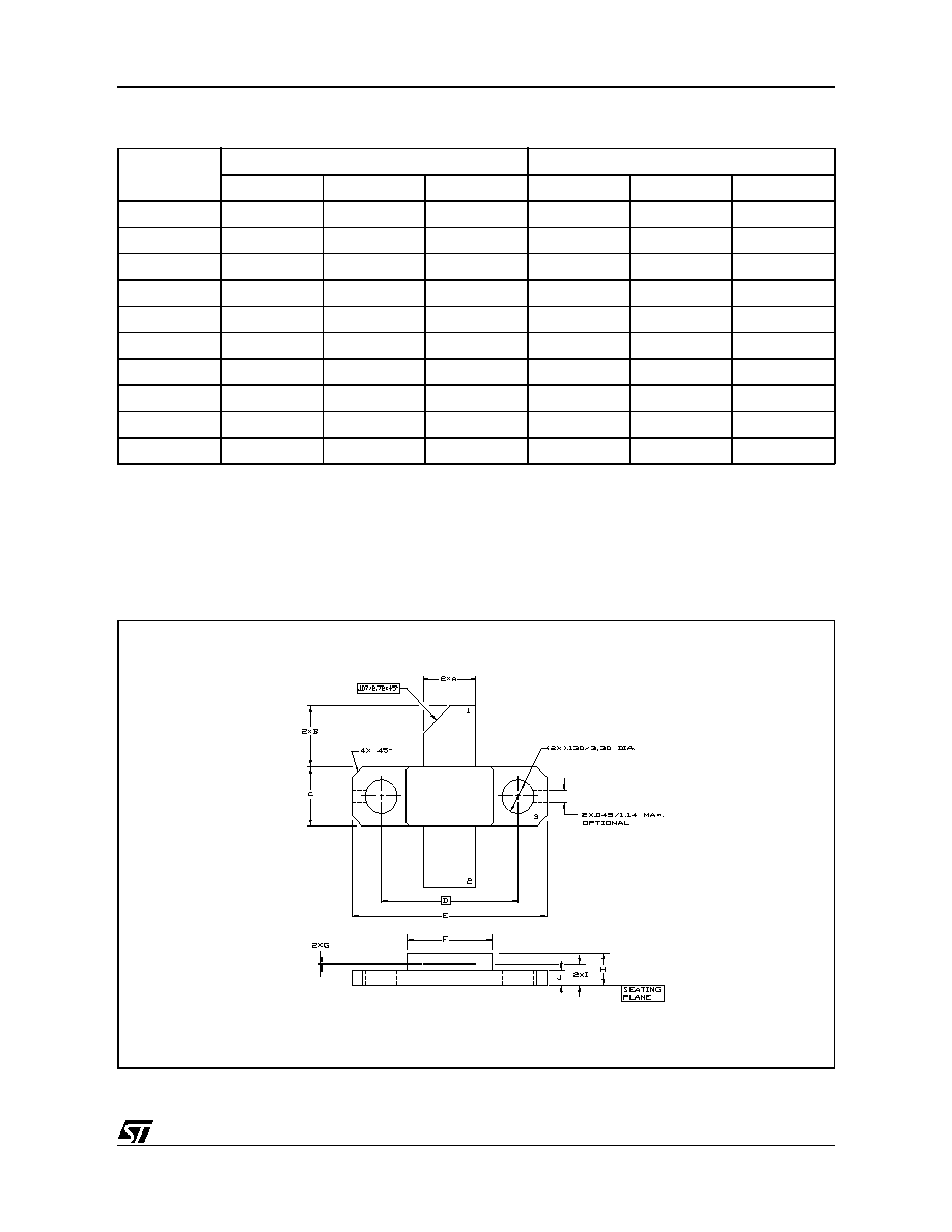
M243
epoxy sealed
ORDER CODE
SD60030
BRANDING
SD60030
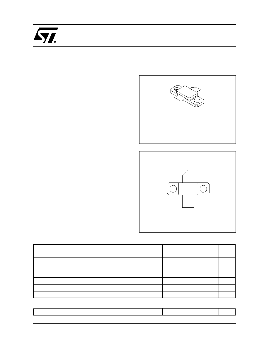
PIN CONNECTION
1
3
2
1. Drain
2. Gate
3. Source

SD60030
4/4
Information furnished is believed to be accurate and reliable. However, STMicroelectronics assumes no responsibility for the consequences
of use of such information nor for any infringement of patents or other rights of third parties which may result from its use. No license is granted
by implication or otherwise under any patent or patent rights of STMicroelectronics. Specifications mentioned in this publication are subject
to change without notice. This publication supersedes and replaces all information previously supplied. STMicroelectronics products are not
authorized for use as critical components in life support devices or systems without express written approval of STMicroelectronics.
The ST logo is registered trademark of STMicroelectronics
Æ
2001 STMicroelectronics - All Rights Reserved
All other names are the property of their respective owners.
Australia - Brazil - Canada - China - Finland - France - Germany - Hong Kong - India - Israel - Italy - Japan -
Malaysia - Malta - Morocco - Singapore - Spain - Sweden - Switzerland - United Kingdom - U.S.A.
http://www.st.com