
SMBYT03
Æ
October 1999 - Ed : 2C
FAST RECOVERY RECTIFIER DIODES
DESCRIPTION
FEATURES
SMC
Symbol
Parameter
Value
Unit
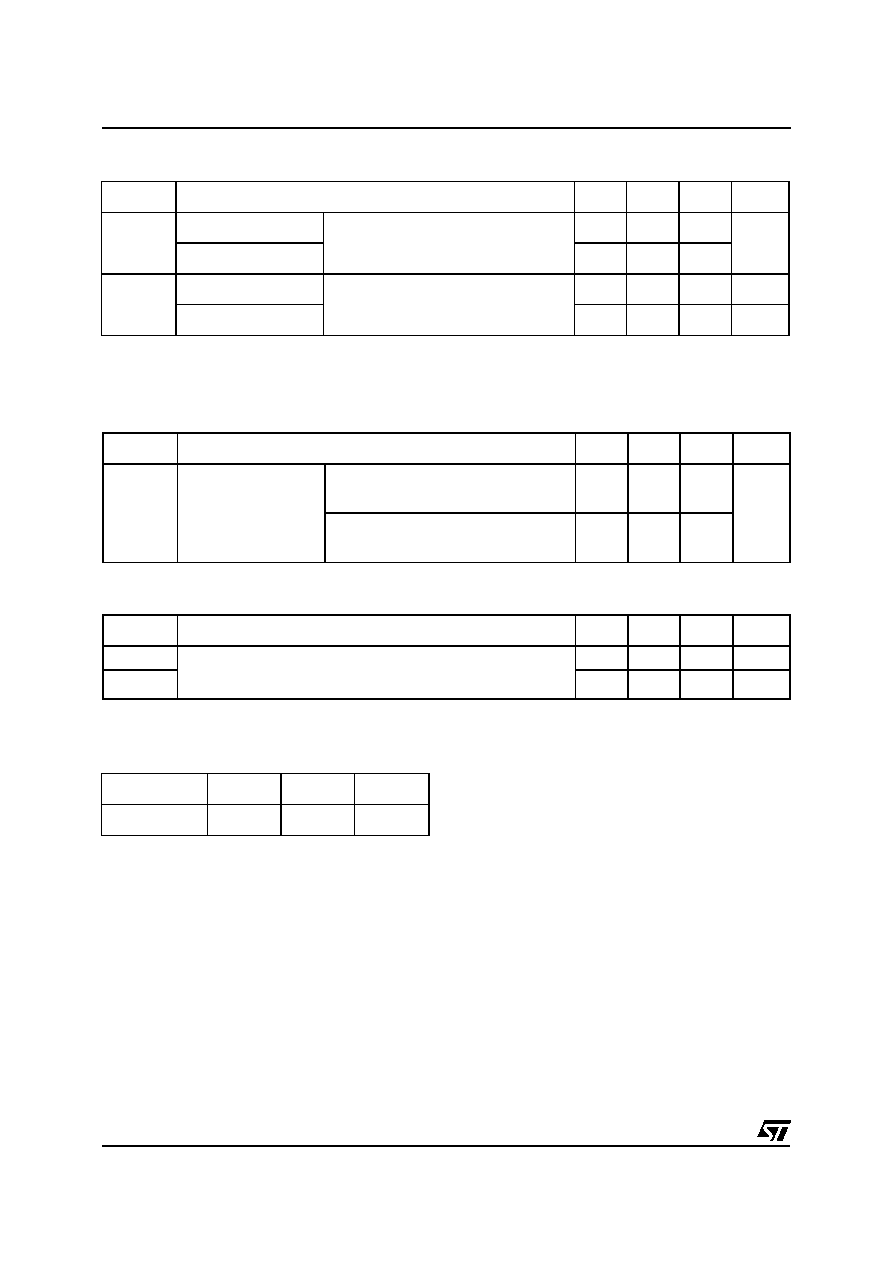
I
F(RMS)
RMS forward current
10
A
I
F(AV)
Average forward current
Tl=55
∞
C
= 0.5
3
A
I
FSM
Non repetitive surge peak forward current
tp=10ms
sinusoidal
60
A
Tstg
Tj
Storage and junction temperature range
- 40 to + 150
- 40 to + 150
∞
C
∞
C
ABSOLUTE MAXIMUM RATINGS
Symbol
Parameter
Value
Unit
V
RRM
Repetitive peak reverse voltage
400
V
Symbol
Parameter
Value
Unit
Rth (j-l)
Junction-leads
20
∞
C/W
THERMAL RESISTANCE
VERY LOW REVERSE RECOVERY TIME
VERY LOW SWITCHING LOSSES
LOW NOISE TURN-OFF SWITCHING
SURFACE MOUNT DEVICE
Single high voltage rectifier ranging from 200V to
400 V suited for Switch Mode Power Supplies and
other power converters.
1/5
Symbol
Test Conditions
Min.
Typ.
Max.
Unit
V
F *
Tj = 25
∞
C
I
F
= 3 A
1.5
V
T
j
= 100
∞
C
1.05
1.4
I
R
**
T
j
= 25
∞
C
V
R
= V
RRM
10
µ
A
T
j
= 100
∞
C
0.2
0.6
mA
Pulse test : * tp = 380
µ
s, duty cycle < 2 %
** tp = 5 ms, duty cycle < 2 %
ELECTRICAL CHARACTERISTICS
STATIC CHARACTERISTICS
Symbol
Test Conditions
Min.
Typ.
Max.
Unit
trr
T
j
= 25
∞
C
I
F
= 0.5A
I
R
= 1A
Irr = 0.25A
25
ns
I
F
= 1A
V
R
= 30V
dI
F
/dt = -15A/
µ
s
60
RECOVERY CHARACTERISTICS
Symbol
Test Conditions
Min.
Typ.
Max.
Unit
t
IRM
V
CC
= 200V I
F
= 3A Lp
0.05
µ
H
T
j
= 100
∞
C dI
F
/dt = -50A/
µ
s
35
50
ns
I
RM
1.5
2
A
To evaluate the conduction losses use the following equation :
P = 1.1 x I
F(AV)
+ 0.08 x I
F
2
(RMS)
TURN-OFF SWITCHING CHARACTERISTICS (Without serie inductance)
Voltage (V)
200
300
400
Marking
C2
C3
C4
Laser marking
Logo indicates cathode
SMBYT03
2/5

0.001
0.01
0.1
1
10
0
2
4
6
8
10
12
14
16
18
20
IM
t
=0.5
t(s)
IM(A)
Tc=25 C
o
Tc=55 C
o
Tc=40 C
o
Fig.3 : Non repetitive surge peak forward current
versus overload duration.
0.001
0.01
0.1
1
10
0.01
0.1
1
Zth(j-c) (tp.
)
K =
Rth(j-c)
= 0 . 5
= 0 . 2
= 0 . 1
Single pulse
tp(s)
T
=tp/T
tp
K
Fig.4 : Relative variation of thermal impedance
junction to lead versus pulse duration.
0.0
0.1
0.2
0.3
0.4
0.5
0.6
0.7
0.8
0.9
1.0
0
10
20
30
40
50
60
P=0.5W
T
I
M
=tp/T
tp
IM(A)
P=1.5W
P=2.5W
Fig.2 : Peak current versus form factor.
0.0
0.5
1.0
1.5
2.0
2.5
3.0
3.5
4.0
0.0
0.5
1.0
1.5
2.0
2.5
3.0
3.5
4.0
4.5
5.0
5.5
=0.05
=0.1
=0.2
=0.5
T
=tp/T
tp
IF(av)(A)
PF(av)(W)
=1
Fig.1 : Low frequency power losses versus
average current.
0
20
40
60
80
100
120
140
160
0.0
0.5
1.0
1.5
2.0
2.5
3.0
3.5
T
=tp/T
tp
=0.5
F(av)(A)
I
o
Tamb( C)
1cm Cu
2
Rth(j-a)=65
C/W
o
Rth(j-a)=Rth(j-l)
Fig.6 : Average current versus ambient
temperature. (duty cycle : 0.5)
0.01
0.1
1
10
0.0
0.3
0.6
0.9
1.2
1.5
1.8
2.1
2.4
2.7
3.0
I FM(A)
VFM(V)
Tl=100
C
o
50
Fig.5 : Voltage drop versus forward current.
(Maximum values)
SMBYT03
3/5

Fig.10 : Recovery charge versus dIF/dt.
(typical values)
Fig.9 : Peak reverse current versus dIF/dt.
Fig.7 : Recovery time versus dI
F
/dt.
Fig.8 : Peak forward voltage versus dI
F
/dt.
0.0 0.5 1.0 1.5 2.0 2.5 3.0 3.5 4.0 4.5 5.0
0
10
20
30
40
50
60
70
80
90
100
Rth(j-a)
2
Scu(cm )
Printed circuit : epoxy (e=35um)
Fig.12 : Thermal resistance junction to ambient
versus copper surface under each lead.
Fig.11 : Dynamic parameters versus junction
temperature.
SMBYT03
4/5

PACKAGE MECHANICAL DATA
SMC
REF.
DIMENSIONS
Millimeters
Inches
Min.
Max.
Min.
Max.
A1
1.90
2.45
0.075
0.096
A2
0.05
0.20
0.002
0.008
b
2.90
3.2
0.114
0.126
c
0.15
0.41
0.006
0.016
E
7.75
8.15
0.305
0.321
E1
6.60
7.15
0.260
0.281
E2
4.40
4.70
0.173
0.185
D
5.55
6.25
0.218
0.246
L
0.75
1.60
0.030
0.063
Information furnished is believed to be accurate and reliable. However, STMicroelectronics assumes no responsibility for the consequences of
use of such information nor for any infringement of patents or other rights of third parties which may result from its use. No license is granted by
implication or otherwise under any patent or patent rights of STMicroelectronics. Specifications mentioned in this publication are subject to
change without notice. This publication supersedes and replaces all information previously supplied.
STMicroelectronics products are not authorized for use as critical components in life support devices or systems without express written ap-
proval of STMicroelectronics.
The ST logo is a registered trademark of STMicroelectronics
© 1999 STMicroelectronics - Printed in Italy - All rights reserved.
STMicroelectronics GROUP OF COMPANIES
Australia - Brazil - China - Finland - France - Germany - Hong Kong - India - Italy - Japan - Malaysia
Malta - Morocco - Singapore - Spain - Sweden - Switzerland - United Kingdom - U.S.A.
http://www.st.com
2.0
4.2
2.0
3.3
FOOTPRINT DIMENSIONS
SMC
E
C
L
E1
D
A1
A2
b
SMBYT03
5/5