1/4
NOT FOR NEW DESIGN
November 2002
This is information on a product still in production but not recommended for new designs.
SSM1105V
Scalar System Memory (SSM)
for Image Processor ICs
FEATURES SUMMARY
s
System solution for use with image processing
scalar ICs
≠ For LCD monitors, projectors, and TVs
≠ Compatible with Pixelworks PW11x/PWx64
families (and similar image processors or mi-
cro-controllers)
s
Single integrated package, including:
≠ Dual bank Flash memories
≠ DDC, I
2
C, and PWM channels
≠ General purpose I/O
≠ Programmable logic
≠ In-System Programming via JTAG
s
Dual bank Flash memories
≠ Provide concurrent operation
≠ 5 Mbit main Flash memory
≠ 384 Kbit secondary Flash memory (divided
into 10 small sectors)
≠ Programmable Decode PLD for flexible ad-
dress mapping of both memories
s
Dual Display Data Channels (DDC)
≠ Supports DDC for both analog RGB and digi-
tal DVI video input channels
≠ DDC1/DDC2B VESA standard compliant
≠ 256 byte SRAM buffer for each DDC channel
s
Dual independent I
2
C channels
≠ Each capable of master or slave operation
≠ Control A/D converters, video decoders, and
future devices (tuner, audio, etc.)
s
Four Pulse Width Modulator (PWM) channels
≠ 16-bit resolution for period and for duty cycle
≠ 16-bit clock prescalers
s
Seven I/O ports with 52 I/O pins for Multifunction
I/O: GPIO, DDC, I
2
C, PWM, PLD I/O, and JTAG
s
3000 gate PLD with 16 macrocells, for creating
glue logic, state machines, clock dividers,
decoders, chip-selects, inverters; and to
prioritize interrupts from DDC, I
2
C, PWM
Figure 1. Packages
s
In-System Programming (ISP) with JTAG
≠ Program entire chip in 30-40 seconds with no
involvement of the processor
≠ Program with low-cost FlashLINK
s
Content Security: Programmable Security Bit
blocks access of device programmers / readers
s
Zero-Power Technology: memory and PLD
blocks automatically switch to stand-by current
between input changes
s
Package and Specifications
≠ 100-pin TQFP, 14 x 14mm
≠ 90 ns memory access time
≠ V
CC
Operating Voltage: 2.7V to 3.6V
TQFP100 (U)
SSM1105V
2/4
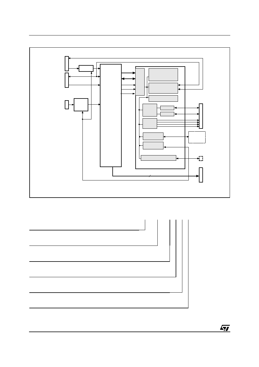
SUMMARY DESCRIPTION
SSM1105V devices bring in-system programma-
ble (ISP) and in-application programmable (IAP)
flash memory to LCD monitor, projector and televi-
sion applications utilizing a scalar IC from either
Pixelworks or other similar image processors or
micro-controllers (MCU). Figure 3 shows a typical
SSM based system with Pixelworks processor.
The SSM1105V devices feature a dual -bank flash
architecture, Dual Display Data Channels (DDC),
I
2
C, PWM channels, general purpose I/O, pro-
grammable logic, and in-system programming via
either JTAG or I
2
C.
The dual-bank Flash memory architecture sup-
ports full concurrent operation permitting IAP in
the field, which means that firmware can be re-
motely updated with little interruption of system
operation. During run-time, the secondary Flash
memory array is ideal for EEPROM emulation,
thus eliminating the need for a separate external
EEPROM.
An on-chip, decode PLD provides for flexible ad-
dress mapping for both memories. Dual 256 byte
SRAMs provide buffer storage for the DDC chan-
nels, thus removing the burden from the proces-
sor.
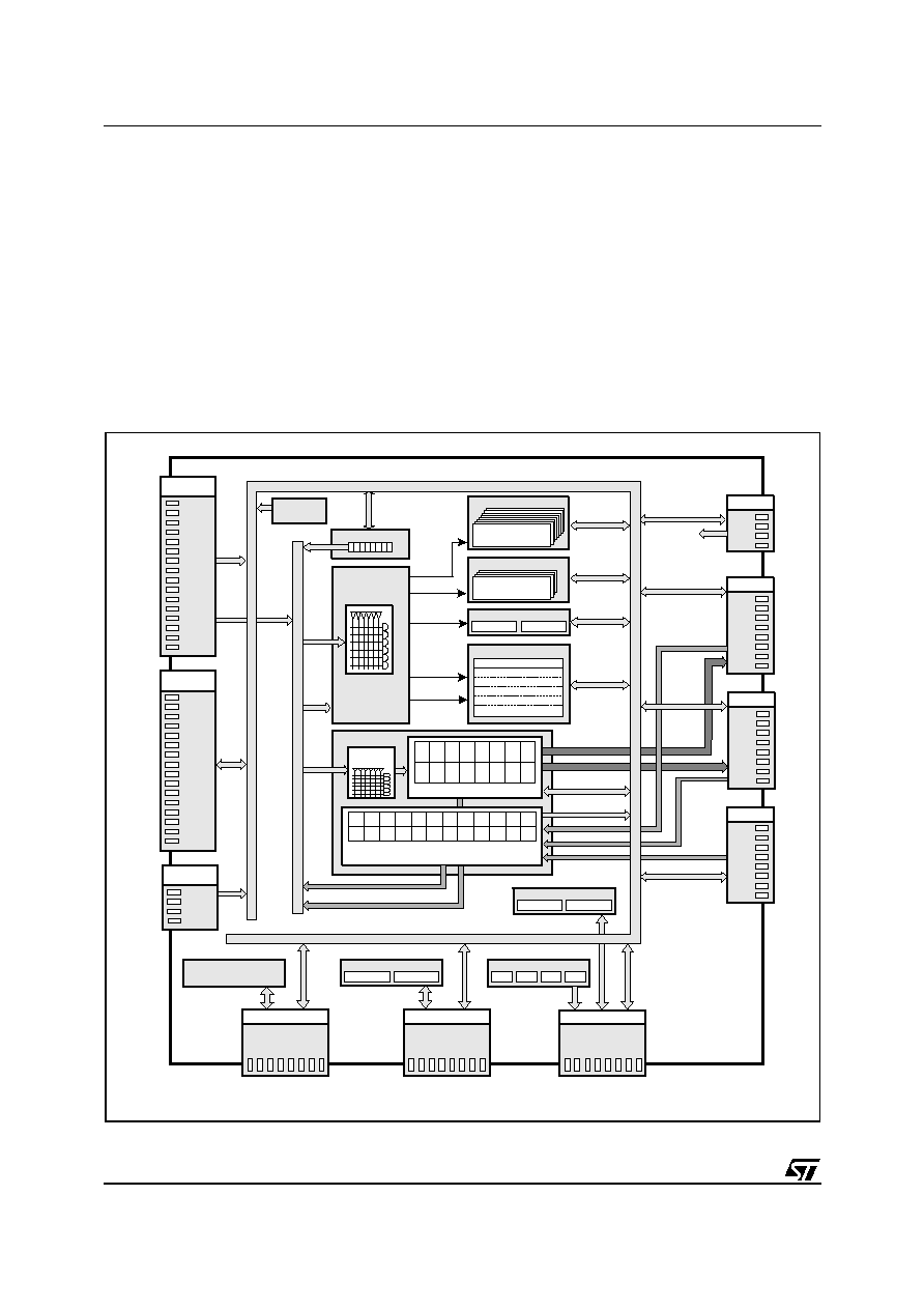
Figure 2. SSM Block Diagram
Note: Additional address lines can be brought in to the device via Port A, B, C or D.
AI04976
PD0
PD1
PD2
I/O PORT
PD3
PA0
PA1
PA2
PA3
PA4
PA5
PA6
PA7
I/O PORT
PB0
PB1
PB2
PB3
PB4
PB5
PB6
PB7
I/O PORT
GENERAL PLD
24 INPUT
MICROCELLS
16 OUTPUT MICROCELLS
A
A
A
A
A
A
A
A
B
B
B
B
B
B
B
B
PAGE REG
SECURITY
LOCK
P
L
D I
N
P
U
T
BU
S
MAIN FLASH
10 BLOCKS, 64 KB
640 KBytes total
PIN FEEDBACK
CSBOOT0-5
NODE FEEDBACK
DECODE
PLD
AND
ARRAY
SECONDARY FLASH
6 BLOCKS, 8 KB
48 KBytes total
FS0-9
A
A
A
A
A
A
A
A
B
B
B
B
B
B
B
B
C
C
C
C
C
C
C
C
TO PLD
IN BUS
RUNTIME CONTROL
REG FILES
DDC
I2C
PWM
GPIO
POWER MNGMT
CSIOP
DDC SRAMs
256 byte
256 byte
DDC-SRAM
PC0
PC1
PC2
PC3
PC4
PC5
PC6
PC7
I/O PORT
P
H
0
P
H
1
P
H
2
P
H
3
P
H
4
P
H
5
P
H
6
P
H
7
I/O PORT
P
I
0
P
I
1
P
I
2
P
I
3
P
I
4
P
I
5
P
I
6
P
I
7
I/O PORT
P
E
0
P
E
1
P
E
2
P
E
3
P
E
4
P
E
5
P
E
6
P
E
7
I/O PORT
DUAL I2C
I2C0
I2C1
QUAD PWM
PW0
PW1
PW2
PW3
JTAG ISP
CONTROLLER
DUAL DDC
DDC0
DDC1
INTERNAL ADDR, DATA, CONTROL BUS LINKED TO CPU
INTERNAL ADDR, DATA, CONTROL BUS LINKED TO CPU
AD0
CPU ADDR
AD1
AD2
AD3
AD4
AD5
AD6
AD7
AD8
AD9
AD10
AD11
AD12
AD13
AD14
AD15
CPU CNTL
CNTL2
RST\
CNTL0
CNTL1
CPU DATA
PF0
PF1
PF2
PF3
PF4
PF5
PF6
PF7
PG0
PG1
PG2
PG3
PG4
PG5
PG6
PG7
CSIP