 | ÐлекÑÑоннÑй компоненÑ: ST1534AD | СкаÑаÑÑ:  PDF PDF  ZIP ZIP |
Äîêóìåíòàöèÿ è îïèñàíèÿ www.docs.chipfind.ru
1/15
April 2003
s
GLITCH FREE TRANSITION BETWEEN
INPUT SOURCES
s
INTERNAL LOGIC SELECTS INPUT
SOURCE
s
GATE DRIVE FOR EXTERNAL PMOS
BYPASS SWITCH
s
5V DETECTOR WITH HYSTERESIS
s
1% 3.3V REGULATED OUTPUT VOLTAGE
s
500mA GUARANTEED OUTPUT CURRENT
s
OPERATING TEMPERATURE RANGE
FROM 0°C TO 85°C
s
AVAILABLE IN P
2
PAK PACKAGE
s
PPAK AND SO-8 PACKAGES CAN BE
AVAILABLE ON REQUEST
APPLICATIONS
s
NETWORK INTERFACE CARDS
s
PCMCIA/PCI INTERFACE CARDS
s
DESKTOP COMPUTERS
s
POWER SUPPLY WITH MULTIPLE INPUT
SOURCES
DESCRIPTION
The ST1534A is intended for application such as
power managed PCI and network interface cards
(NICs), where operations from 3.3V VAUX supply
may be required when the 5V supply has been
shut down.
During regular operation, 3.3V power for the PCI
card is provided by the internal LDO regulator,
generated from 5V supply. When the 5V V
AUX
is
available, the IC connects this supply directly to its
output using an external P-Channel FET. This
ensures an uninterrupted 3.3V out even if VIN falls
out of specification.
When both supplies are available simultaneously,
the drive pin DR will be pulled high, turning off the
PMOS switch.
The device is available in the popular 5 leads
P
2
PAK and PPAK
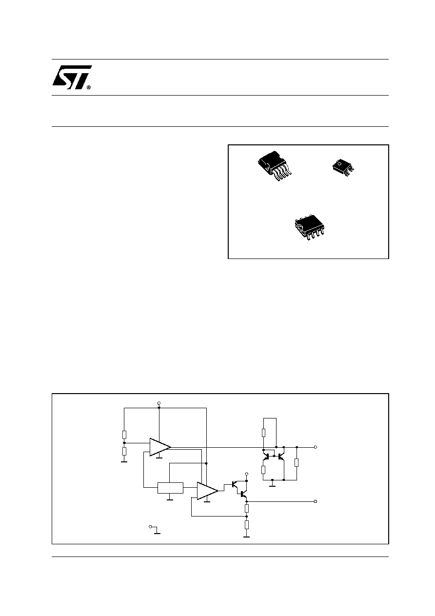
ST1534A
500mA SMART LDO
-
+
-
+
V
IN
V
IN
DR
V
OUT
Reference
Error
Amp
5V Detect
Rpull_down
GND
SCHEMATIC DIAGRAM
SO-8
PPAK
P
2
PAK
ST1534A
2/15
ABSOLUTE MAXIMUM RATINGS
Absolute Maximum Ratings are those values beyond which damage to the device may occur. Functional operation under these condition is
not implied.
THERMAL DATA
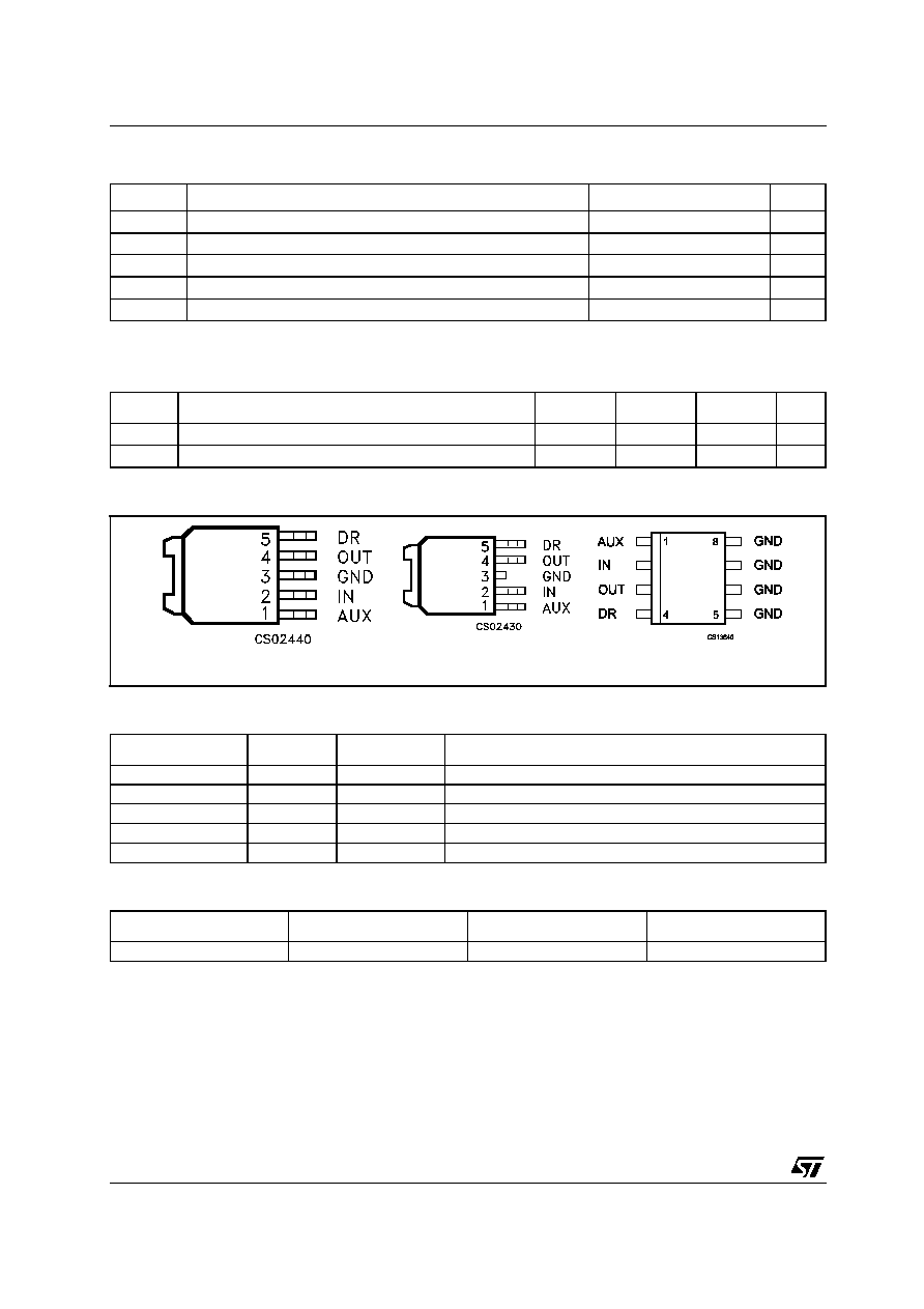
CONNECTION DIAGRAM (top view)
PIN DESCRIPTION
ORDERING INFORMATION
(*) PPAK and SO-8 are available in Tape & Reel with the suffix "-TR".
(#) P
2
PAK is available in Tape & Reel with the suffix "-R".
Symbol
Parameter²
Value
Unit
V
I
DC Input Voltage
-0.3 to 7
V
V
SHDN
Shutdown Input Voltage
-0.3 to 7
V
I
O
Output Current
Internally limited
mA
T
stg
Storage Temperature Range
-40 to +125
°C
T
op
Operating Junction Temperature Range
0 to +85
°C
Symbol
Parameter
PPAK
P
2
PAK
SO-8
Unit
R
thj-case
Thermal Resistance Junction-case
8
3
20
°C/W
R
thj-amb
Thermal Resistance Junction-ambient
100
50
55
°C/W
SO-8
P
2
PAK
PPAK
Pin PPAK/P
2
PAK
Pin SO/8
Symbol
Name and Function
1
1
AUX
Auxiliary Input port typically 3.3V
2
2
IN
Input port typically 5V
3
5, 6, 7, 8
GND
Ground
4
3
OUT
LDO 3.3V Output Port
5
4
DR
Drive Output for external P-Channel MOSFET pass element
TYPE
PPAK (*)
P
2
PAK (#)
SO-8 (*)
ST1534A
ST1534APT
ST1534AP2T
ST1534AD
ST1534A
3/15
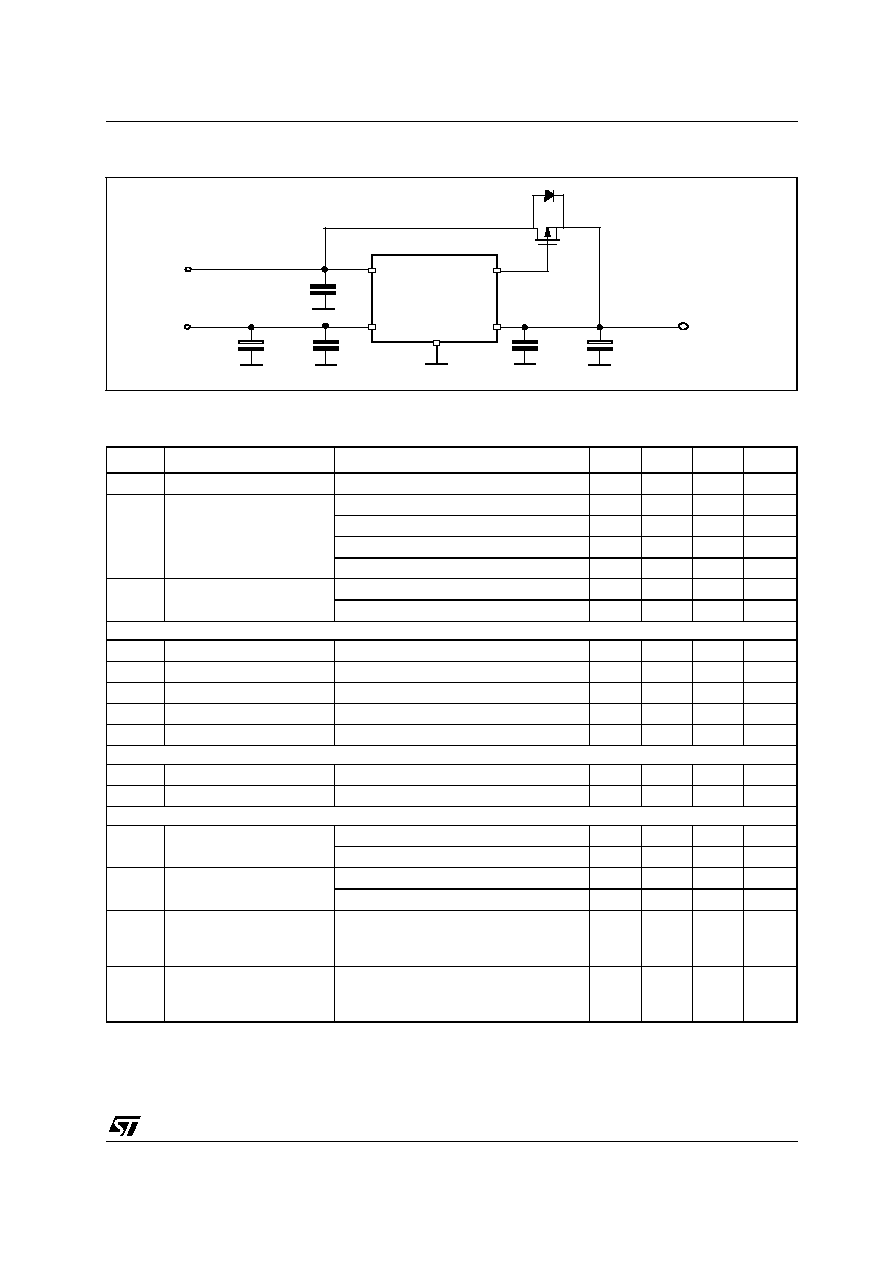
TYPICAL APPLICATION CIRCUIT
ELECTRICAL CHARACTERISTICS (T
j
= 25°C, V
I
=5V, V
AUX
=3.3V, I
O
=10mA, C
O
= 2.2
µ
F,
unless otherwise specified)
Note 1: Guaranteed by design
Note 2: See timing diagram
Symbol
Parameter
Test Conditions
Min.
Typ.
Max.
Unit
V
I
Input Voltage Range
4.5
5
5.5
V
I
IN
Input Supply Current
V
I
4.5V
I
O
= 0mA
V
AUX
= 0V
11
mA
V
I
4.5V
I
O
= 0mA
V
AUX
= 3.3V
11
mA
V
I
< 4.1V
I
O
= 0mA
V
AUX
= 0V
2
mA
V
I
< 4.1V
I
O
= 0mA
V
AUX
= 3.3V
2
mA
I
AUX
Auxliary Supply Current
V
I
= 0 V
2.2
mA
V
I
= 5V
200
µ
A
3.3V VOLTAGE REGULATOR BLOCK
V
O
Output Voltage
T
j
= 0 to 85 °C
3.18
3.3
3.42
V
V
O
Line Regulation
V
I
= 4.5 to 5.5V
0.04
0.5
%
V
O
Load Regulation
I
O
= 0 to 500mA
0.1
1
%
V
d
Dropout Voltage
I
O
= 500 mA T
j
= 0 to 85 °C
1.15
V
I
O
Output Current Limit
T
j
= 0 to 85 °C
550
mA
5V DETECT BLOCK
V
THL
Low Threshold Voltage
V
I
falling,
I
O
= 500 mA T
j
= 0 to 85 °C
4.15
4.3
V
V
HYST
Hysteresis
70
200
mV
DRIVE OUTPUT BLOCK
V
DR
Drive Output Voltage
V
I
= 4.5 to 5.5V
I
DR
= 200
µ
A
3.6
V
IN
-0.8
V
V
I
< 4.15V
I
DR
= 200
µ
A
100
200
mV
I
DR
Drive Current
Sinking: V
I
= 4.15V
V
DR
= 1V
7
20
mA
Sourcing: V
I
= 4.5V
V
I
- V
DR
= 2V
7
25
mA
t
DH
Drive High Delay (Note 1
and 2)
C
DR
= 1.2nF, V
IN
ramping up, measured
from V
I
= V
TH(H)
to V
DR
= 3.3V
T
j
= 0 to 85 °C
2
5
µ
s
t
DL
Drive Low Delay (Note 1
and 2)
C
DR
= 1.2nF, V
IN
ramping down, measured
from V
I
= V
TH(L)
to V
DR
= 200mV
T
j
= 0 to 85 °C
3
6
µ
s
IN
GND
OUT
DR
4.7 µF
0.1 µF
5V
3.3V
10 µF
0.1 µF
Vout=3.3V
0.1 µF
AUX
ST1534A
4/15
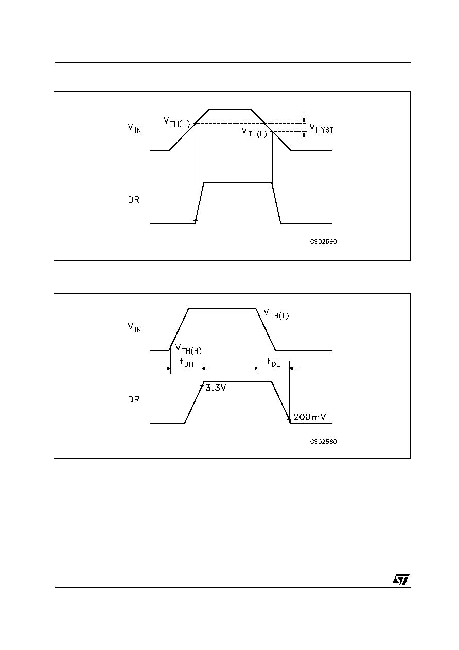
5V DETECT THRESHOLDS
V
IN
rise and fall times (10% to 90%) to be > 100
µ
s
TIMING DIAGRAM
V
IN
rise and fall times (10% to 90%) to be > 100
µ
s
ST1534A
5/15
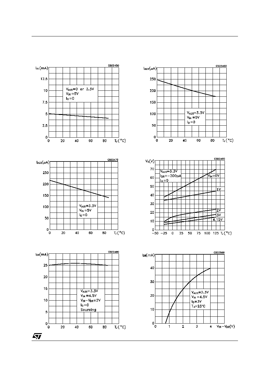
TYPICAL CHARACTERISTICS (unless otherwise specified T
j
= 25°C)
Figure 1 : Supply Current vs Temperature
Figure 2 : Aux Current vs Temperature
Figure 3 : Drive Current vs Temperature
Figure 4 : Aux Current vs Temperature
Figure 5 : Drive Output Voltage vs Temperature
Figure 6 : Drive Current vs V
IN
-V
DR