1/20
October 2004
s
HIGH SPEED: t
PD
= 4.4ns (MAX.) at T
A
=85∞C
V
CCA
= 3.0V V
CCB
= 2.3V
s
LOW POWER DISSIPATION:
I
CCA
= I
CCB
= 20
µ
A(MAX.) at T
A
=85∞C
s
SYMMETRICAL OUTPUT IMPEDANCE:
|I
OHA
| = I
OLA
= 8mA MIN at
V
CCA
= 3.0V V
CCB
= 1.65V or 2.3V
|I
OHB
| = I
OLB
= 6mA MIN at
V
CCB
= 1.65V V
CCA
= 3V)
s
BALANCED PROPAG. DELAYS: t
PLH
t
PHL
s
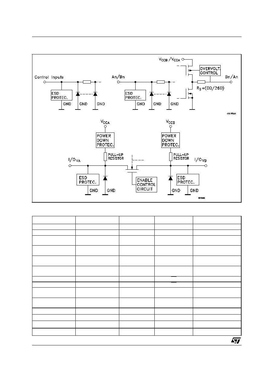
POWER DOWN PROTECTION ON I/O
s
26
SERIES RESISTOR ON A SIDE OUTPUTS
s
OPERATING VOLTAGE RANGE:
V
CCA
(OPR)=2.3V to 3.6V (1.2V Data Retent)
V
CCB
(OPR)=1.65V to 2.7V (1.2V Data Retent)
s
FAST I
2
C LINES 1.8V/2.8V LEVEL
TRANSLATOR: 400KHz GUARANTEED
DATA RATE AT C
L
= 15pF
s
BUS HOLD PROVIDED ON DATA INPUT
BOTH SIDE
s
LATCH-UP PERFORMANCE EXCEEDS
500mA (JESD 17)
s
ESD PERFORMANCE:
HBM > 2000V (MIL STD 883 method 3015);
MM > 200V
DESCRIPTION
The ST16C32245 is a dual supply low voltage
CMOS 14-BIT BUS TRANSCEIVER fabricated
with sub-micron silicon gate and five-layer metal
wiring C
2
MOS technology. Designed for use as an
interface between a 3.3V bus and a 2.5V or 1.8V
bus in a mixed 3.3V/1.8V,3.3V/2.5V and 2.5V/
1.8V supply systems, it achieves high speed
operation while maintaining the CMOS low power
dissipation and it includes 2-bit I
2
C level
translation. This IC is intended for two-way
asynchronous communication between data
buses and the direction of data transmission is
determined by nDIR inputs. The enable inputs nG
can be used to disable the device so that the
buses are effectively isolated. The A-port
interfaces with the 3V bus, the B-port with the 2.5V
and 1.8V bus. All inputs are equipped with
protection circuits against static discharge, giving
them 2KV ESD immunity and transient excess
voltage. All floating bus terminals during High Z
State don't need external pull-up or pull-down
resistor.
ST16C32245
14 BIT DUAL SUPPLY BUS TRANSCEIVER LEVEL
TRANSLATOR, A SIDE SERIES RESISTOR, 2 BIT I
2
C LINES
This is preliminary information on a new product now in development or undergoing evaluation. Details are subject to change without notice.
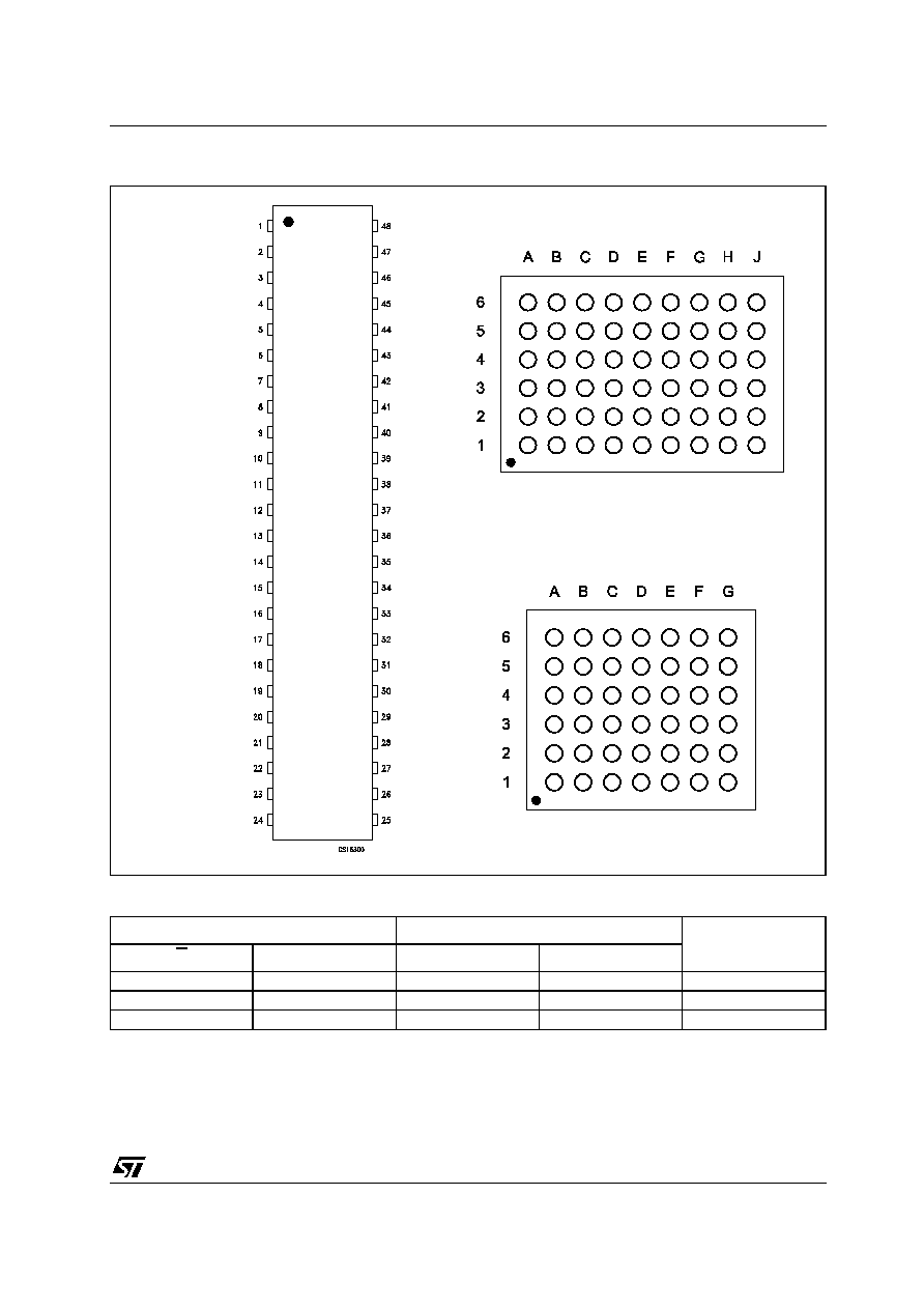
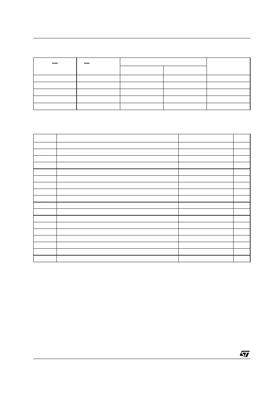
Table 1: Order Codes
PACKAGE
T & R
TSSOP48
ST16C32245TTR
TFBGA54
ST16C32245LBR
µ
TFBGA42
ST16C32245TBR
TSSOP
µ
TFBGA
TFBGA
PRELIMINARY DATA
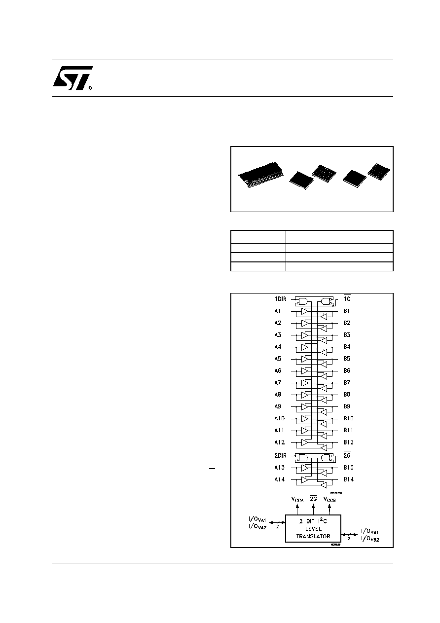
Figure 1: Logic Diagram
Rev. 1
ST16C32245
4/20
Table 4: I
2
C Bus Function Table
Open: If I/O
VA
is not driven then the I/O
VB
will go in high level V
CCB
by embedded 10k
pull-up resistor; If I/O
VB
is not driven then the I/O
VA
will go in high level V
CCB
by embedded 10k
pull-up resistor.
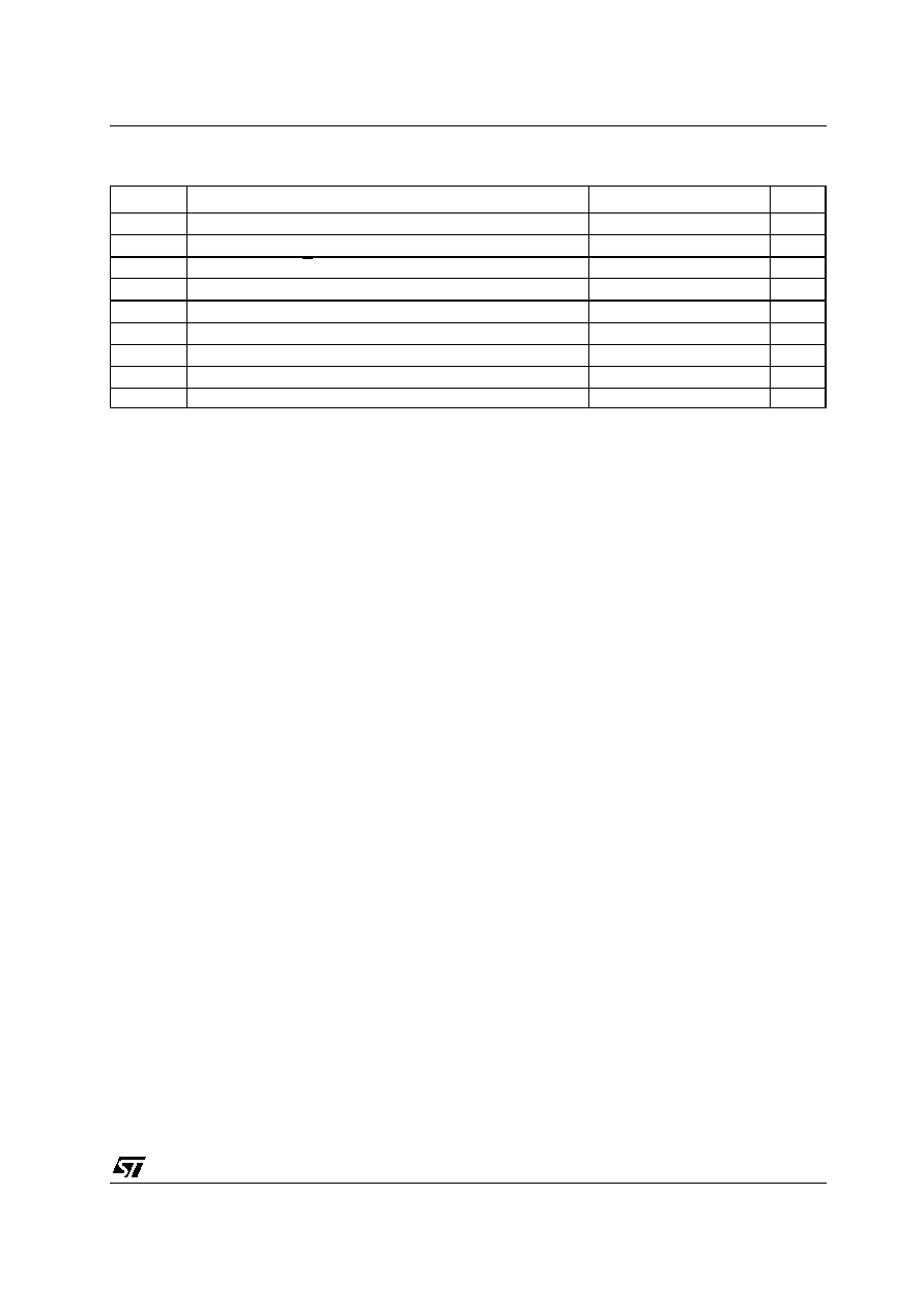
Table 5: Absolute Maximum Ratings
Absolute Maximum Ratings are those value beyond which damage to the device may occur. Functional operation under these conditions is
not implied
2G
1G, 1DIR, 2DIR
I/O INPUT
FUNCTION
I/O
VA
I/O
VB
H
X
Z
Z
I
2
C Disabled
L
X
L
L
I
2
C Comm.
L
X
V
CCA
V
CCB
I
2
C Comm.
L
X
Open
V
CCB
I
2
C Comm.
L
X
V
CCA
Open
I
2
C Comm.
Symbol
Parameter
Value
Unit
V
CCA
Supply Voltage
-0.5 to +4.6
V
V
CCB
Supply Voltage
-0.5 to +4.6
V
V
I
DC Input Voltage
-0.5 to +4.6
V
V
I/OA
DC I/O Voltage (Output disabled)
-0.5 to +4.6
V
V
I/OB
DC I/O Voltage (Output disabled)
-0.5 to +4.6
V
V
I/OA
DC I/O Voltage
-0.5 to V
CCA
+ 0.5
V
V
I/OB
DC I/O Voltage
-0.5 to V
CCB
+ 0.5
V
V
I/OVA
Level Input Voltage (I/O
VA
)
-0.5 to V
CCA
+ 0.5
V
V
I/OVB
Level Input Voltage (I/O
VB
)
-0.5 to V
CCB
+ 0.5
V
I
IK
DC Input Diode Current
-
20
mA
I
OK
DC Output Diode Current
-
50
mA
I
OA
DC Output Current
±
50
mA
I
OB
DC Output Current
±
50
mA
I
CCA
DC V
CC
or Ground Current
±
100
mA
I
CCB
DC V
CC
or Ground Current
±
100
mA
P
d
Power Dissipation
400
mW
T
stg
Storage Temperature
-65 to +150
∞C
T
L
Lead Temperature (10 sec)
260
∞C