12 January 98
42 1714 01
The information in this datasheet is subject to change
1/66
ST18952
DIGITAL SIGNAL PROCESSOR (DSP) CHIP
PRELIMINARY DATA
s
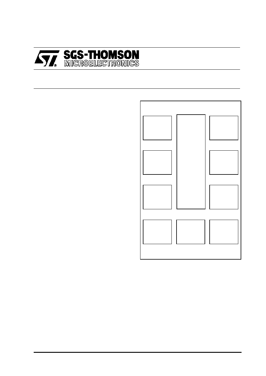
Programmable D950 Core
s
Data calculation unit
s
Address calculation unit
s
Program control unit
s
Fast and flexible buses
s
66MIPS - 15 ns instruction cycle time
s
16.5 Kwords data memory (RAM)
s
32 Kwords program memory (RA42 1714 01)
s
Interrupt controller
s
DMA controller
s
Serial input/output
s
Timer
s
Bus switch unit
s
Emulation unit
s
JTAG IEEE 1149.1 test access port
TAP
Emulation
unit
2
Timers
2
Serial I/O
Interrupt
controller
16.5 Kwords
data memory
Bus switch
unit
DMA
controller
D950
core
32 Kwords
program
memory

2/66
Table of Contents
3
1
Introduction . . . . . . . . . . . . . . . . . . . . . . . . . . . . . . . . . . . . . . . . . . . . . . . . . . . . . . . . . . 4
2
Pin Description . . . . . . . . . . . . . . . . . . . . . . . . . . . . . . . . . . . . . . . . . . . . . . . . . . . . . . . 5
3
Functional Overview . . . . . . . . . . . . . . . . . . . . . . . . . . . . . . . . . . . . . . . . . . . . . . . . . . . 9
4
D950Core . . . . . . . . . . . . . . . . . . . . . . . . . . . . . . . . . . . . . . . . . . . . . . . . . . . . . . . . . . 12
4.1
D950Core registers . . . . . . . . . . . . . . . . . . . . . . . . . . . . . . . . . . . . . . . . . . . . . . . 14
5
Memory . . . . . . . . . . . . . . . . . . . . . . . . . . . . . . . . . . . . . . . . . . . . . . . . . . . . . . . . . . . . 15
5.1
Internal memory resource . . . . . . . . . . . . . . . . . . . . . . . . . . . . . . . . . . . . . . . . . . 15
5.2
Direct bus extension . . . . . . . . . . . . . . . . . . . . . . . . . . . . . . . . . . . . . . . . . . . . . . 16
6
Bus Switch Unit . . . . . . . . . . . . . . . . . . . . . . . . . . . . . . . . . . . . . . . . . . . . . . . . . . . . . . 18
6.1
BSU operation . . . . . . . . . . . . . . . . . . . . . . . . . . . . . . . . . . . . . . . . . . . . . . . . . . . 18
6.2
BSU control registers . . . . . . . . . . . . . . . . . . . . . . . . . . . . . . . . . . . . . . . . . . . . . . 19
7
DMA Controller . . . . . . . . . . . . . . . . . . . . . . . . . . . . . . . . . . . . . . . . . . . . . . . . . . . . . . 21
7.1
DMA operation . . . . . . . . . . . . . . . . . . . . . . . . . . . . . . . . . . . . . . . . . . . . . . . . . . . 22
7.2
DMA registers . . . . . . . . . . . . . . . . . . . . . . . . . . . . . . . . . . . . . . . . . . . . . . . . . . . 23
8
Interrupt Controller . . . . . . . . . . . . . . . . . . . . . . . . . . . . . . . . . . . . . . . . . . . . . . . . . . . . 26
8.1
Interrupt controller registers . . . . . . . . . . . . . . . . . . . . . . . . . . . . . . . . . . . . . . . . . 27
9
Timers . . . . . . . . . . . . . . . . . . . . . . . . . . . . . . . . . . . . . . . . . . . . . . . . . . . . . . . . . . . . . 31
9.1
Timer registers . . . . . . . . . . . . . . . . . . . . . . . . . . . . . . . . . . . . . . . . . . . . . . . . . . . 31
10 SIO . . . . . . . . . . . . . . . . . . . . . . . . . . . . . . . . . . . . . . . . . . . . . . . . . . . . . . . . . . . . . . . 35
10.1 SIO registers . . . . . . . . . . . . . . . . . . . . . . . . . . . . . . . . . . . . . . . . . . . . . . . . . . . . 35
11 External Coprocessor . . . . . . . . . . . . . . . . . . . . . . . . . . . . . . . . . . . . . . . . . . . . . . . . . 41
12 System Control . . . . . . . . . . . . . . . . . . . . . . . . . . . . . . . . . . . . . . . . . . . . . . . . . . . . . . 41
12.1 System registers . . . . . . . . . . . . . . . . . . . . . . . . . . . . . . . . . . . . . . . . . . . . . . . . . 42
12.2 Clocks . . . . . . . . . . . . . . . . . . . . . . . . . . . . . . . . . . . . . . . . . . . . . . . . . . . . . . . . . 44
13 JTAG IEEE 1149.1 test access port . . . . . . . . . . . . . . . . . . . . . . . . . . . . . . . . . . . . . . 45
14 Emulation Unit . . . . . . . . . . . . . . . . . . . . . . . . . . . . . . . . . . . . . . . . . . . . . . . . . . . . . . . 45
15 Electrical Specifications . . . . . . . . . . . . . . . . . . . . . . . . . . . . . . . . . . . . . . . . . . . . . . . . 47
15.1 DC Absolute maximum ratings . . . . . . . . . . . . . . . . . . . . . . . . . . . . . . . . . . . . . . 47
15.2 DC Electrical characteristics . . . . . . . . . . . . . . . . . . . . . . . . . . . . . . . . . . . . . . . . 47
15.3 AC Characteristics . . . . . . . . . . . . . . . . . . . . . . . . . . . . . . . . . . . . . . . . . . . . . . . . 48
16 Y SPACE Memory Mapping . . . . . . . . . . . . . . . . . . . . . . . . . . . . . . . . . . . . . . . . . . . . 56
16.1 Memory map . . . . . . . . . . . . . . . . . . . . . . . . . . . . . . . . . . . . . . . . . . . . . . . . . . . . 56
16.2 Serial input/output registers . . . . . . . . . . . . . . . . . . . . . . . . . . . . . . . . . . . . . . . . . 56
16.3 Timer registers . . . . . . . . . . . . . . . . . . . . . . . . . . . . . . . . . . . . . . . . . . . . . . . . . . . 58
16.4 Bus switch unit registers . . . . . . . . . . . . . . . . . . . . . . . . . . . . . . . . . . . . . . . . . . . 58
1

3/66
Table of Contents
16.5 System control registers . . . . . . . . . . . . . . . . . . . . . . . . . . . . . . . . . . . . . . . . . . . 58
16.6 DMA controller registers . . . . . . . . . . . . . . . . . . . . . . . . . . . . . . . . . . . . . . . . . . . 59
16.7 Interrupt controller registers . . . . . . . . . . . . . . . . . . . . . . . . . . . . . . . . . . . . . . . . . 59
16.8 Emulation unit registers . . . . . . . . . . . . . . . . . . . . . . . . . . . . . . . . . . . . . . . . . . . . 60
16.9 D950Core control registers . . . . . . . . . . . . . . . . . . . . . . . . . . . . . . . . . . . . . . . . . 60
17 ST18952 Package Specifications . . . . . . . . . . . . . . . . . . . . . . . . . . . . . . . . . . . . . . . . 61
17.1 208 pin PQFP pinout . . . . . . . . . . . . . . . . . . . . . . . . . . . . . . . . . . . . . . . . . . . . . . 61
17.2 208 pin PQFP package dimensions . . . . . . . . . . . . . . . . . . . . . . . . . . . . . . . . . . 62
18 Device ID . . . . . . . . . . . . . . . . . . . . . . . . . . . . . . . . . . . . . . . . . . . . . . . . . . . . . . . . . . . 64
19 Ordering Information . . . . . . . . . . . . . . . . . . . . . . . . . . . . . . . . . . . . . . . . . . . . . . . . . . 64
20 Revision History . . . . . . . . . . . . . . . . . . . . . . . . . . . . . . . . . . . . . . . . . . . . . . . . . . . . . . 64

4/66
ST18952
1
Introduction
The ST18952 chip includes the SGS-Thomson D950 16-bit fixed point digital signal processor
core, 16.5 Kwords of data memory, 32 Kwords of program memory, and the following on-chip
peripherals:
�
Interrupt controller (ITC)
�
DMA controller (DMA)
�
Bus switch unit (BSU)
�
Synchronous input/output (SIO)
�
Timer (TIM)
�
Emulation unit (EMU)
�
Tap controller (TAP)
It also includes an oscillator and a PLL for generation of the D950Core clock.
The ST18952 is used on the D950 Emulation Card (called the D952 module) developed by
SGS-Thomson.
It can also be used for application development by customers.
Custom development is eased by providing direct access to the D950 instruction and data
buses to allow simultaneous access to external memories or peripherals (with wait-states).
For full details of the D950Core refer to the D950Core datasheet (
document number 42-1709).
2
5/66
ST18952
2
Pin Description
The following tables detail the ST18952 pin set. There is one table for each group of pins. The
tables detail the pin name, type and a short description of the pin function.
Signal names have an overbar if they are active low, otherwise they are active high.
Table 2.1
Direct I bus extension (35 pins)
Table 2.2
Direct Y bus extension (35 pins)
Table 2.3
Direct X bus extension / bus extension through bus switch unit (39 pins)
Pin name
Type
Description
IDE0-15
I/O
Instruction data extension bus.
IAE0-15
O
Instruction address extension bus.
IRDE
O
I-extension bus read strobe. Active low.
IWRE
O
I-extension bus write strobe. Active low.
IBSE
O
I-extension bus strobe. Active low.
Pin name
Type
Description
YDE0-15
I/O
Y data extension bus.
YAE0-15
O
Y address extension bus.
YRDE
O
Y-extension bus read strobe. Active low.
YWRE
O
Y-extension bus write strobe. Active low.
YBSE
O
Y-extension bus strobe. Active low.
Pin name
Type
Description
ED_XDE0-15
I/O
Multiplexed input/output. Bus switch unit extension data bus or X data exten-
sion bus.
EA_XAE0-15
O
Multiplexed output. Bus switch unit extension address bus or X address ex-
tension bus.
EIRD
O
BSU EIRD output
EIWR
O
BSU EIWR output
XBSE
O
X extension bus data strobe
EYRD
O
BSU EYRD output
EYWR
O
BSU EYWR output
XRDE_EXRD
O
Multiplexed output.
X-extension bus read strobe (XRDE) or BSU EXRD output.
XWRE_EXWR
O
Multiplexed output.
X-extension bus write strobe (XWRE) or BSU EXWR output.