1/11
February 2005
I
ADJUSTABLE OUTPUT VOLTAGE FROM
0.8V to V
I
-V
d
I
INTERNAL REFERENCE VOLTAGE
ACCURACY ± 2% AT 25°C
I
OUTPUT CURRENT CAPABILITY: 1A
MINIMUM
I
VERY LOW QUIESCENT CURRENT: MAX
3mA OVER TEMPERATURE RANGE
I
MAXIMUM DROPOUT 1V (@ I
O
=1A)
I
STABLE ONLY WITH LOW ESR CERAMIC
CAPACITORS
I
THERMAL SHUTDOWN PROTECTION
WITH HYSTERESIS
I
OVER CURRENT PROTECTION
I
OPERATING JUNCTION TEMPERATURE
RANGE: FROM 0 TO 125°C
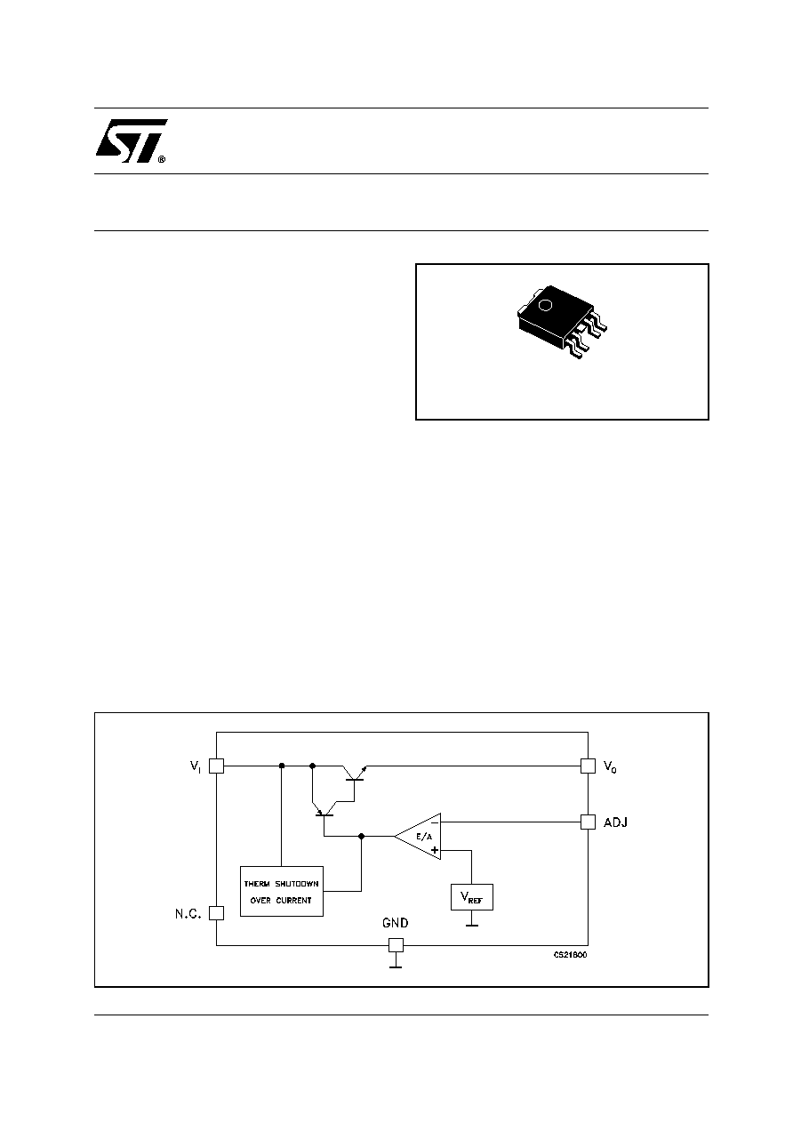
DESCRIPTION
The ST1L04 is a low drop adjustable linear
voltage regulator capable to supply up to 1A
output current.
The output voltage can be as low as 0.8V. The
quiescent current is well controlled and
maintained below 3mA over the whole allowed
junction temperature range. The ST1L04 is stable
only with low ESR output ceramic capacitors.
Internal protection circuitry includes thermal
protection with hysteresis and over current
limiting.
The ST1L04 is especially suitable for applications
requiring low voltage outputs from low voltage
inputs. Typical application for this product are,
notebook PCs, low voltage ASIC, VID power
supplies and low cost post regulation for 3.3V
output voltage switching regulators.
ST1L04
LOW QUIESCENT CURRENT VOLTAGE REGULATOR
Figure 1: Schematic Diagram
PPAK
Rev. 1
ST1L04
2/11
Table 1: Order Codes
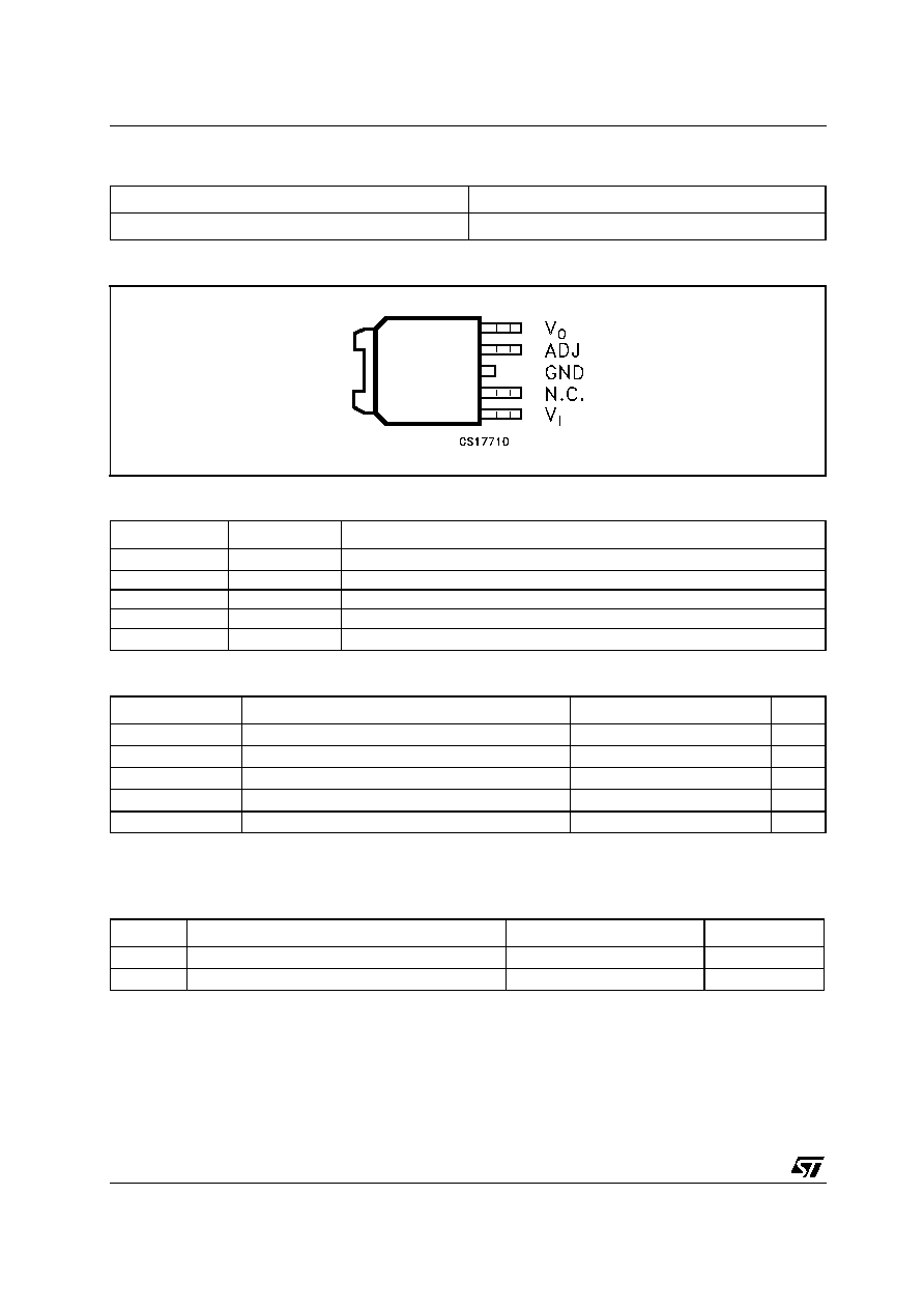
Figure 2: Pin Connection (top view)
Table 2: Pin Description
Table 3: Absolute Maximum Ratings
Absolute Maximum Ratings are those values beyond which damage to the device may occur. Functional operation under these condition is
not implied.
Table 4: Thermal Data
TYPE
PPAK
ST1L04
ST1L04PT
PIN N°
NAME
FUNCTION
1
V
I
Supply voltage input pin. Bypass with a ceramic capacitor to GND
2
N.C.
Not connected.
3
GND
Ground. The exposed metallic pad of the package is connected to GND.
4
ADJ
Adjust voltage pin. External resistor divider connection.
5
V
O
Output voltage pin. Bypass with a ceramic capacitor to GND
Symbol
Parameter
Value
Unit
V
I
DC Supply Voltage
from GND-0.3 to 10
V
P
tot
Power Dissipation
internally limited
W
I
O
Output Current
internally limited
A
T
op
Operating Junction Temperature Range
0 to +125
°C
T
stg
Storage Temperature Range
-40 to +150
°C
Symbol
Parameter
PPAK
Unit
R
thj-case
Thermal Resistance Junction-case
8
°C/W
R
thj-amb
Thermal Resistance Junction-ambient
100
°C/W
ST1L04
3/11
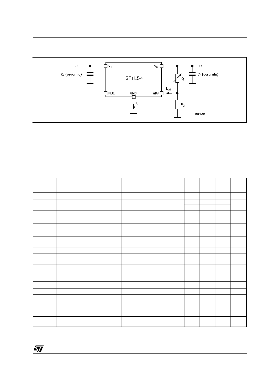
Figure 3: Typical Application Schematic
NOTE: The adjustable output voltage is set by a resistor divider connected between V
O
and GND with its centre tap connected to ADJ. The
voltage divider resistor are: R1 connected between V
O
and ADJ and R2 connected between ADJ and GND. V
O
is determined by V
REF
, R1,
R2, I
ADJ
, as follows:
V
O
=V
REF
(1+R1/R2)+I
ADJ
R1
Since I
ADJ
is very small and stable it can be ignored and the output voltage can be simply calculated as follows:
V
O
=V
REF
(1+R1/R2)
Table 5: Electrical Characteristics (refer to the typical application schematic, V
IN
=from 2.9 to 5.5V, I
O
=
from 10mA to 1A,
C
IN
=4.7µF, C
OUT
=4.7µF, T
j
=0 to 125°C, unless otherwise specified). Typical values
are intended at T
j
=25°C unless otherwise specified
NOTE 1: This parameter is the minimum input to output differential voltage required to maintain 1% regulation with respect to the V
O
nominal
value. For V
O
between 0.8V and 1.8V included, the V
d
value is overridden by the minimum operating input voltage.
NOTE 2: Guaranteed by design. Not tested in production.
Symbol
Parameter
Test Conditions
Min.
Typ.
Max.
Unit
V
I
Operating Input Voltage
2.8
V
I
d
Quiescent Current
3
mA
V
REF
Reference Voltage
T
J
= 25°C
0.784
0.8
0.816
V
0.776
0.8
0.824
V
O
Line Regulation
I
O
= 10mA
0.8
%
V
O
Load Regulation
V
I
= 3.3V
0.8
%
I
ADJ
Adjustment Current
I
O
= 10mA
1
µA
I
ADJ
Adjustment Current change
200
nA
I
Omin
Minimum Output Current for
regulation
100
µA
I
O
Output Current Limit
1
1.4
A
V
d
Dropout Voltage
(see note 1 and note 2)
I
O
= 1A, V
O
= from 1.8 to 3.3V
1
V
SVR
Supply Voltage Rejection
(see note 2)
V
I
= 3.3±0.5V,
I
O
=10mA,
T
J
= 25°C
f=120Hz
50
dB
f=100kHz
20
C
O
Ceramic Output capacitor value
2.2
µF
C
ESR
Output Capacitor ESR value
200
m
eN
Output Noise Voltage (see note 2)
B = from 10Hz to 10kHz,
V
I
= 3.3V, I
O
=10mA, T
j
=25°C
0.003
%V
O
T
SH
Thermal shutdown trip point
(see note 2)
V
I
=3.3V
165
°C
T
HY
Thermal Shutdown hysteresis
(see note 2)
V
I
=3.3V
5
°C
ST1L04
4/11
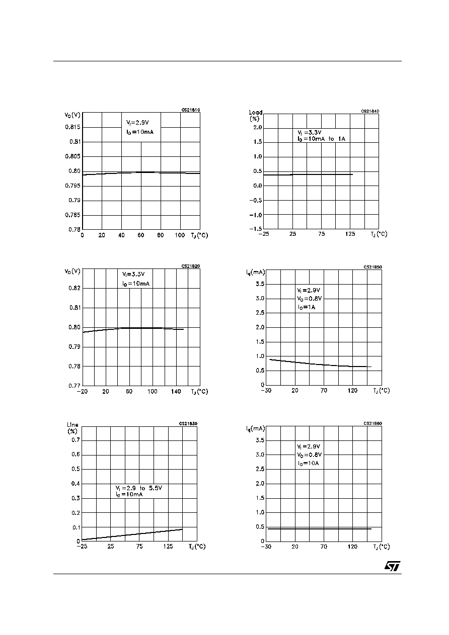
TYPICAL CHARACTERISTICS
Figure 4: Output Voltage vs Temperature
Figure 5: Output Voltage vs Temperature
Figure 6: Line Regulation vs Temperature
Figure 7: Load Regulation vs Temperature
Figure 8: Quiescent Current vs Temperature
Figure 9: Quiescent Current vs Temperature
ST1L04
5/11
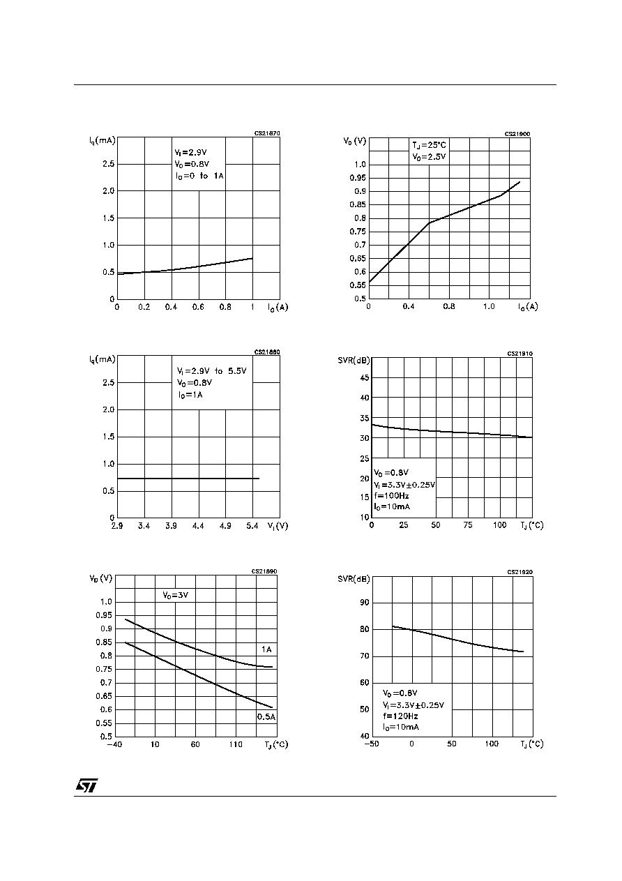
Figure 10: Quiescent Current vs Output Current
Figure 11: Quiescent Current vs Input Voltage
Figure 12: Dropout Voltage vs Temperature
Figure 13: Dropout Voltage vs Output Current
Figure 14: Supply Ripple Rejection vs
Temperature
Figure 15: Supply Ripple Rejection vs
Temperature