 | –≠–ª–µ–∫—Ç—Ä–æ–Ω–Ω—ã–π –∫–æ–º–ø–æ–Ω–µ–Ω—Ç: ST2042 | –°–∫–∞—á–∞—Ç—å:  PDF PDF  ZIP ZIP |
1/8
October 2003
s
80m
HIGH-SIDE MOSFET SWITCH
s
500mA CONTINUOUS CURRENT PER
CHANNEL
s
INDEPENDENT THERMAL AND
SHORT-CIRCUIT PROTECTION WITH
OVERCURRENT LOGIC OUTPUT
s
OPERATING RANGE FROM 2.7V TO 5.5V
s
CMOS- AND TTL-COMPATIBLE ENABLE
INPUTS
s
2.5ms TYPICAL RISE TIME
s
UNDERVOLTAGE LOCKOUT
s
10
µ
A MAXIMUM STANDBY SUPPLY
CURRENT
s
AMBIENT TEMPERATURE RANGE, 0∞C TO
85∞C
s
ESD PROTECTION
DESCRIPTION
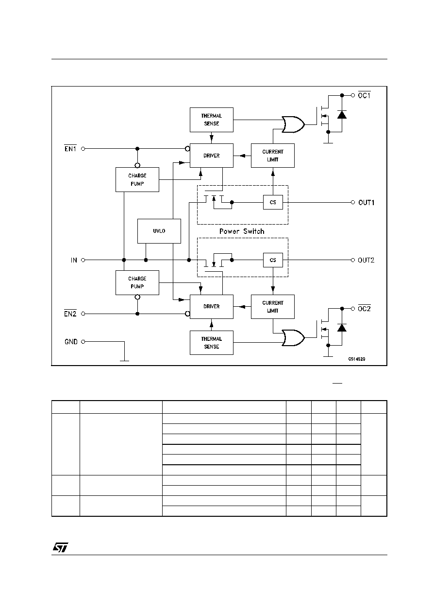
The
ST2042
power
distribution
switches
is
intended for application where heavy capacitive
loads
and
short
circuits
are
likely
to
be
encountered. These devices incorporate 80m
N-channel MOSFET high-side power switches for
power-distribution systems that require multiple
powers switches in a single package. Each switch
is controlled by an independent logic enable input.
Gate drive is provided by an internal charge pump
designed to control the power-switch rise times
and fall times to minimize current surges during
switching. The charge pump requires no external
components and allows operation from supplies
as low as 2.7 V.
When the output load exceeds the current-limit
threshold or a short is present, these devices limit
the output current to a safe level by switching into
a constant-current mode, pulling the overcurrent
(OCx) logic output low. When continuous heavy
overloads and short circuits increase the power
dissipation in the switch, causing the junction
temperature to rise, a thermal protection circuit
shuts off the switch to prevent damage. Recovery
from a thermal shutdown is automatic once the
device has cooled sufficiently. Internal circuitry
ensures the switch remains off until valid input
voltage
is
present.
These
power-distribution
switches are designed to current limit at 0.9 A
ORDERING CODES
Type
Temperature
Range
Package
Comments
ST2042BD
-40 to 85 ∞C
SO-8 (Tube)
50parts per tube / 40tube per box
ST2042BDR
-40 to 85 ∞C
SO-8 (Tape & Reel)
2500 parts per reel
ST2042
CURRENT LIMITED
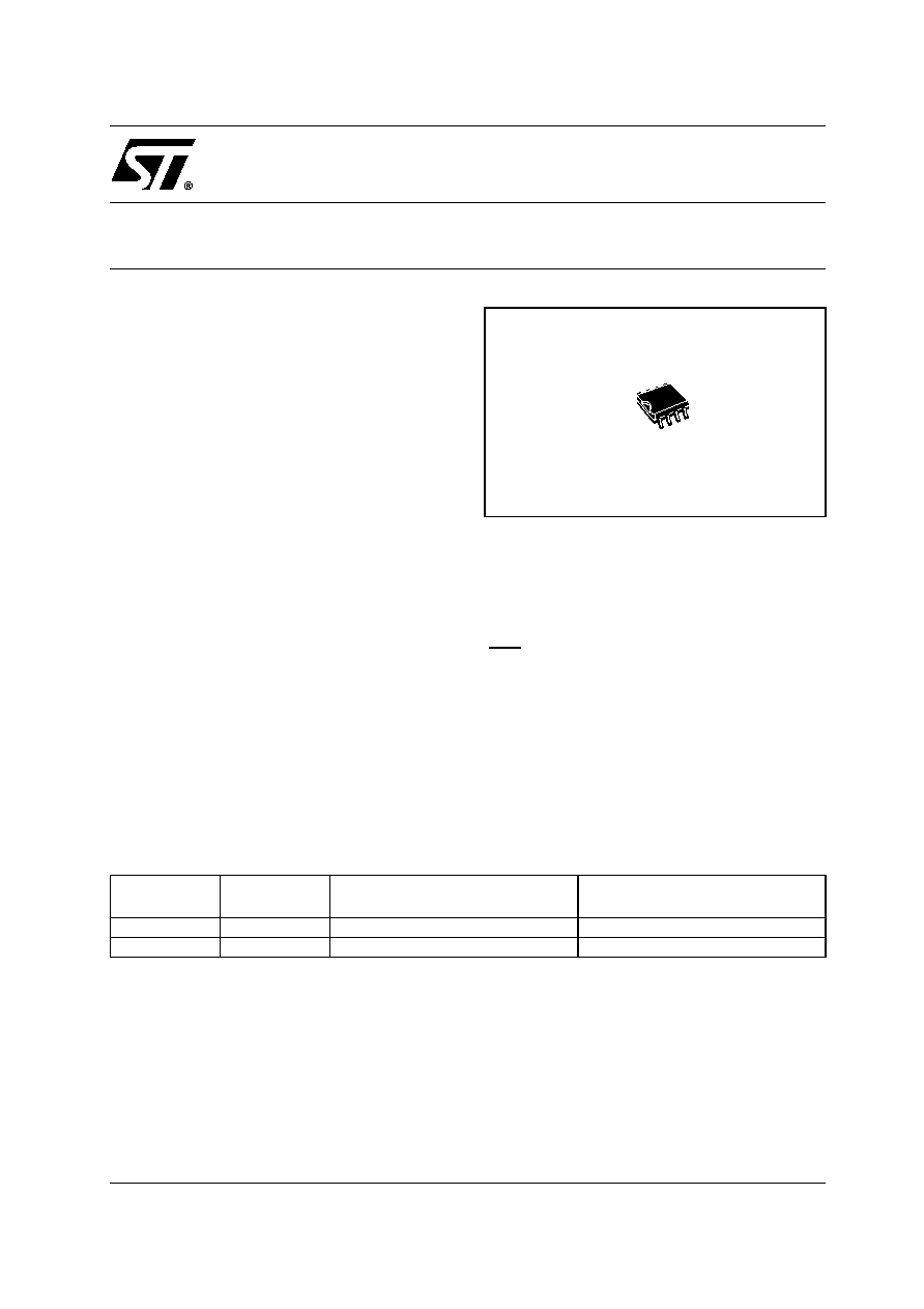
POWER DISTRIBUTION SWITCHES
SOP

ST2042
2/8
PIN CONFIGURATION
PIN DESCRIPTION
ABSOLUTE MAXIMUM RATINGS
Absolute Maximum Ratings are those values beyond which damage to the device may occur. Functional operation under these condition is
not implied.
Note1: All voltage are referred to GND
RECOMMENDED OPERATING CONDITION
Pln N∞
Symbol
Name And Function
1
GND
Ground
2
IN
Input Voltage
3
EN1
Enable Input. Logic Low Turns
On Power Switch IN-OUT1
4
EN2
Enable Input. Logic Low Turns
On Power Switch IN-OUT2
5
OC2
Overcurrent. Logic Output
Active Low IN-OUT2
6
OUT2
Power Switch Output
7
OUT1
Power Switch Output
8
OC1
Overcurrent. Logic Output
Active Low IN-OUT2
Symbol
Parameter
Value
Unit
V
I
Input Voltage Range (Note 1)
-0.3 to 6
V
V
O
Output Voltage Range (Note 1)
-0.3 to (V
I
+0.3)
V
V
IENX
Input Voltage Range
-0.3 to 6
V
I
O
Continuous Output Current
Internally Limited
ESD
Electrostatic Discharge
2
kV
T
J
Operating Junction Temperature
-40 to 125
∞C
Symbol
Parameter
Min.
Typ.
Max.
Unit
V
I
Input Voltage Range (Note 1)
2.7
5.5
V
V
O
Output Voltage Range (Note 1)
0
5.5
V
I
O
Continuous Output Current (Per Switch)
0
500
mA
ST2042
3/8
BLOCK DIAGRAM
POWER SWITCH ELECTRICAL CHARACTERISTICS (V
I
= 5.5V, I
O
= rated current, V
IEN
= 0V, T
J
=
25∞C, unless otherwise specified.) (See Note 1)
Symbol
Parameter
Test Conditions
Min.
Typ.
Max.
Unit
R
DS(ON)
Static Drain-Source
ON-State Resistance
V
I
=5V
I
O
= 0.5A
80
100
m
V
I
=5V
I
O
= 0.5A
T
J
=85∞C
90
120
V
I
=5V
I
O
= 0.5A
T
J
=125∞C
100
135
V
I
=3.3V I
O
= 0.5A
90
125
V
I
=3.3V I
O
= 0.5A
T
J
=85∞C
110
145
V
I
=3.3V I
O
= 0.5A
T
J
=125∞C
120
160
t
r
Output Rise Time
V
I
=5.5V R
L
=10
C
L
=1
µ
F
2.5
ms
V
I
=2.7V R
L
=10
C
L
=1
µ
F
3
t
f
Output Fall Time
V
I
=5.5V R
L
=10
C
L
=1
µ
F
0.3
ms
V
I
=2.7V R
L
=10
C
L
=1
µ
F
0.2
ST2042
4/8
ENABLE INPUT ENx CHARACTERISTICS (V
I
= 5.5V, I
O
= rated current, V
IEN
= 0V, T
J
= 25∞C, unless
otherwise specified.) (See Note 1)
CURRENT LIMIT CHARACTERISTICS (V
I
= 5.5V, I
O
= rated current, V
IEN
= 0V, T
J
= 25∞C, unless
otherwise specified.) (See Note 1)
SUPPLY CURRENT CHARACTERISTICS (V
I
= 5.5V, I
O
= rated current, V
IEN
= 0V, T
J
= 25∞C, unless
otherwise specified.) (See Note 1)
UNDERVOLTAGE CHARACTERISTICS (V
I
= 5.5V, I
O
= rated current, V
IEN
= 0V, T
J
= 25∞C, unless
otherwise specified.) (See Note 1)
OVERCURRENT (OC) CARACTERISTICS (V
I
= 5.5V, I
O
= rated current, V
IEN
= 0V, T
J
= 25∞C, unless
otherwise specified.) (See Note 1)
Note 1: Pulse testing techniques maintain junction temperature close to ambient temperature: thermal effect must be takes into account
separately.
Note 2: Specified by design, not production tested.
Symbol
Parameter
Test Conditions
Min.
Typ.
Max.
Unit
V
IH
High level Input Voltage
V
I
=2.7V to 5.5V
2
V
V
IL
Low level Input Voltage
V
I
=4.5V to 5.5V
0.8
V
V
I
=2.7V to 4.5V
0.4
I
I
Input Current
V
IENX
=0V or V
I
-0.5
0.5
µ
A
t
on
Turn-on Time
R
L
=10
C
L
=100
µ
F
20
ms
t
off
Turn-off Time
R
L
=10
C
L
=100
µ
F
40
ms
Symbol
Parameter
Test Conditions
Min.
Typ.
Max.
Unit
I
OS
Short Circuit Output Current V
I
=5V, OUT connected to GND, device
enabled into short circuit
0.7
1
1.3
A
Symbol
Parameter
Test Conditions
Min.
Typ.
Max.
Unit
I
SOL
Current Low Level Output
V
IENX
= V
I
, No Load,
0.025
1
µ
A
V
IENX
= V
I
, No Load,
T
J
=-40 to 125∞C
10
I
SOH
Current Low High Output
V
IENX
= 0, No Load,
70
90
µ
A
V
IENX
= 0, No Load,
T
J
=-40 to 125∞C
100
I
L
Output Leakage Current
V
IENX
= V
I
, Output Connected to GND,
T
J
=-40 to 125∞C
10
µ
A
Symbol
Parameter
Test Conditions
Min.
Typ.
Max.
Unit
V
IL
Low Level Input Voltage
2
2.5
V
V
HYS
Hysteresis
100
mV
Symbol
Parameter
Test Conditions
Min.
Typ.
Max.
Unit
I
SINK
Sink Current
V
O
=5V
10
mA
V
O
Output Low Voltage
I
O
=5mA
0.5
V
I
OFF
OFF-State Current
V
O
=5V V
O
=3.3V
1
µ
A

ST2042
5/8
TEST CIRCUIT
WAVEFORM: PROPAGATION DELAYS (f=1MHz; 50% duty cycle)
ST2042
6/8
DIM.
mm.
inch
MIN.
TYP
MAX.
MIN.
TYP.
MAX.
A
1.35
1.75
0.053
0.069
A1
0.10
0.25
0.04
0.010
A2
1.10
1.65
0.043
0.065
B
0.33
0.51
0.013
0.020
C
0.19
0.25
0.007
0.010
D
4.80
5.00
0.189
0.197
E
3.80
4.00
0.150
0.157
e
1.27
0.050
H
5.80
6.20
0.228
0.244
h
0.25
0.50
0.010
0.020
L
0.40
1.27
0.016
0.050
k
∞ (max.)
ddd
0.1
0.04
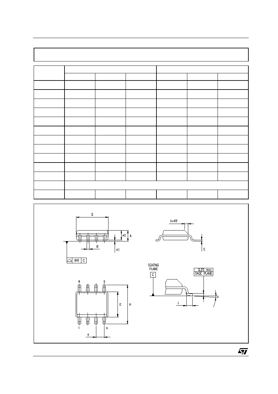
SO-8 MECHANICAL DATA
0016023/C
8
ST2042
7/8
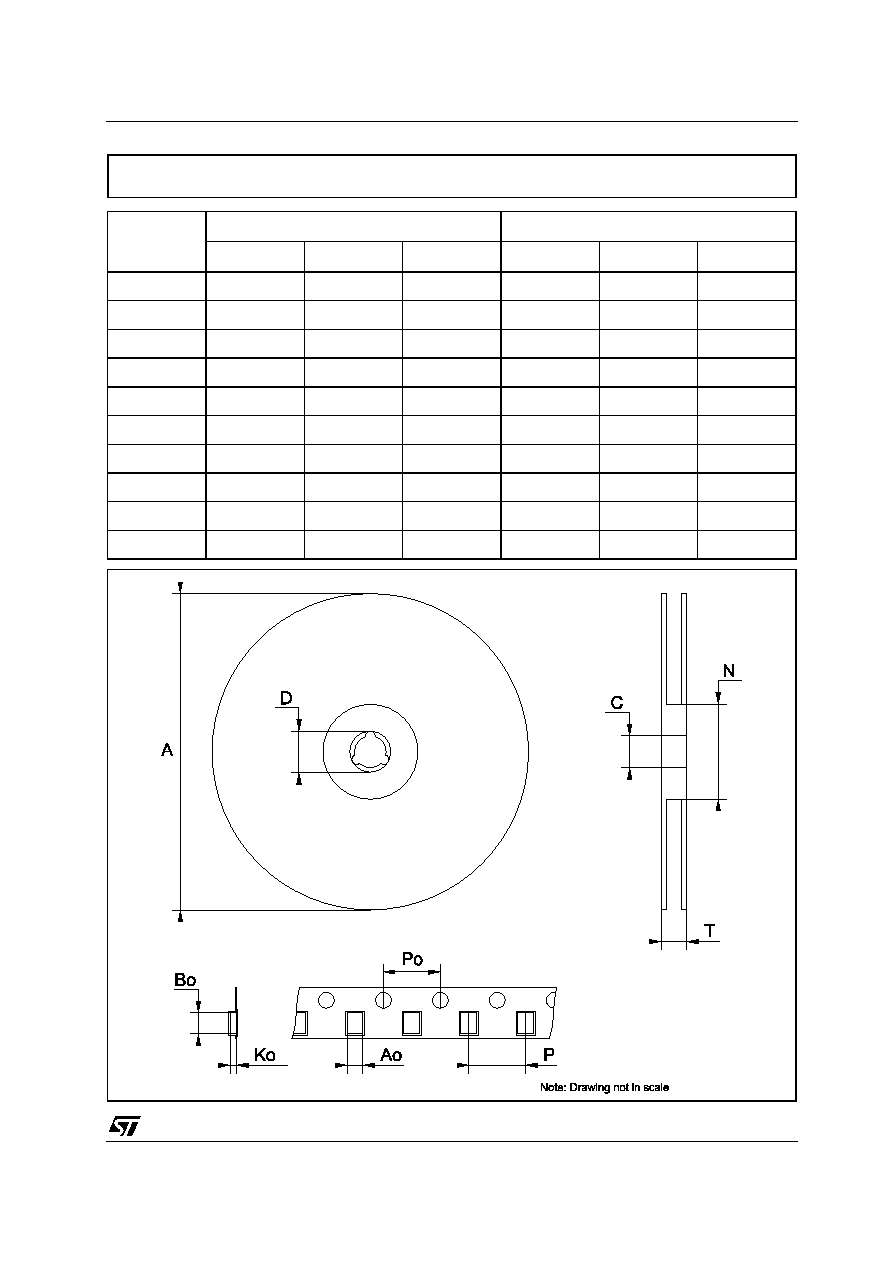
DIM.
mm.
inch
MIN.
TYP
MAX.
MIN.
TYP.
MAX.
A
330
12.992
C
12.8
13.2
0.504
0.519
D
20.2
0.795
N
60
2.362
T
22.4
0.882
Ao
8.1
8.5
0.319
0.335
Bo
5.5
5.9
0.216
0.232
Ko
2.1
2.3
0.082
0.090
Po
3.9
4.1
0.153
0.161
P
7.9
8.1
0.311
0.319
Tape & Reel SO-8 MECHANICAL DATA

ST2042
8/8
Information furnished is believed to be accurate and reliable. However, STMicroelectronics assumes no responsibility for the
consequences of use of such information nor for any infringement of patents or other rights of third parties which may result from
its use. No license is granted by implication or otherwise under any patent or patent rights of STMicroelectronics. Specifications
mentioned in this publication are subject to change without notice. This publication supersedes and replaces all information
previously supplied. STMicroelectronics products are not authorized for use as critical components in life support devices or
systems without express written approval of STMicroelectronics.
The ST logo is a registered trademark of STMicroelectronics
All other names are the property of their respective owners
© 2003 STMicroelectronics - All Rights Reserved
STMicroelectronics GROUP OF COMPANIES
Australia - Belgium - Brazil - Canada - China - Czech Republic - Finland - France - Germany - Hong Kong - India - Israel - Italy - Japan -
Malaysia - Malta - Morocco - Singapore - Spain - Sweden - Switzerland - United Kingdom - United States.
http://www.st.com