 | –≠–ª–µ–∫—Ç—Ä–æ–Ω–Ω—ã–π –∫–æ–º–ø–æ–Ω–µ–Ω—Ç: ST207EATR | –°–∫–∞—á–∞—Ç—å:  PDF PDF  ZIP ZIP |

1/12
September 2003
s
ESD PROTECTION FOR RS-232 I/O PINS:
±
15 KV HUMAN BODY MODEL
s
230kbps DATE RATE
s
GUARANTEED SLEW RATE 3V/
µ
s (Min)
s
OPERATES FROM A SINGLE 5V POWER
SUPPLY
s
PACKAGED IN SO-24, SSO-24 AND
TSSOP24
DESCRIPTION
The ST207E is a 5 driver and 3 receiver devices
designed for RS-232 and V.28 communications in
harsh environments. Each transmitter output and
receiver
input
is
protected
against
±
15KV
electrostatic discharge (ESD) shocks. The drivers
and receivers of the ST207E meet all EIA/
TIA-232E and CCITT V.28 specifications at data
rates up to 120Kbps, when loaded in accordance
with the EIA/TIA-232E specification.
The ST207E operates with four 0.1
µ
F capacitors.
It came in 24-pin SO and TSSOP packages.
ORDERING CODES
Type
Temperature
Range
Package
Comments
ST207ECD
0 to 70 ∞C
SO-24 (Tube)
33parts per tube / 25tube per box
ST207EBD
-40 to 85 ∞C
SO-24 (Tube)
33parts per tube / 25tube per box
ST207EAD
-40 to 125 ∞C
SO-24 (Tube)
33parts per tube / 25tube per box
ST207ECDR
0 to 70 ∞C
SO-24 (Tape & Reel)
1000 parts per reel
ST207EBDR
-40 to 85 ∞C
SO-24 (Tape & Reel)
1000 parts per reel
ST207EADR
-40 to 125 ∞C
SO-24 (Tape & Reel)
1000 parts per reel
ST207ECPR
0 to 70 ∞C
SSOP-24 (Tape & Reel)
1350 parts per reel
ST207EBDR
-40 to 85 ∞C
SSOP-24 (Tape & Reel)
1350 parts per reel
ST207EAPR
-40 to 125 ∞C
SSOP-24 (Tape & Reel)
1350 parts per reel
ST207ECTR
0 to 70 ∞C
TSSOP24 (Tape & Reel)
2500 parts per reel
ST207EBTR
-40 to 85 ∞C
TSSOP24 (Tape & Reel)
2500 parts per reel
ST207EATR
-40 to 125 ∞C
TSSOP24 (Tape & Reel)
2500 parts per reel
ST207E
±
15KV ESD PROTECTED
5V RS-232 TRANSCEIVER
SSOP
SOP
TSSOP
ST207E
2/12
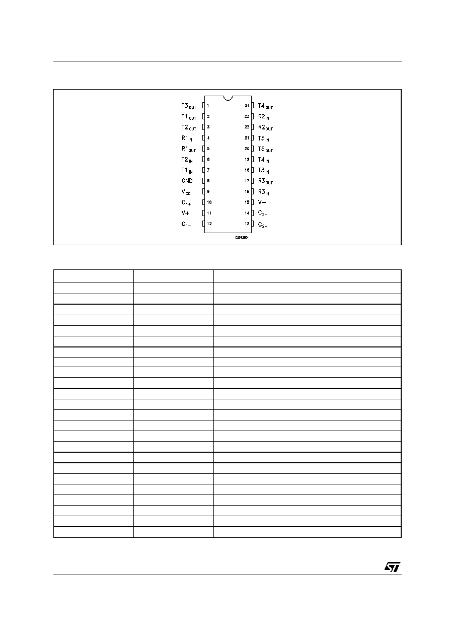
PIN CONFIGURATION
PIN DESCRIPTION
PlN N∞
SYMBOL
NAME AND FUNCTION
1
T3
OUT
RS-232 Driver Output
2
T1
OUT
RS-232 Driver Output
3
T2
OUT
RS-232 Driver Output
4
R1
IN
RS-232 Receiver Input
5
R1
OUT
TTL/CMOS Receiver Output
6
T2
IN
TTL/CMOS Driver Input Internal Pull-up to V
CC
7
T1
IN
TTL/CMOS Driver Input Internal Pull-up to V
CC
8
GND
Ground
9
V
CC
4.75V to 5.25V Supply Voltage
10
C
1+
Terminal For Positive Charge-pump Capacitor
11
V
+
2V
CC
Generated by The Charge-pump
12
C
1-
Terminal For Negative Charge-pump Capacitor
13
C
2+
Terminal For Positive Charge-pump Capacitor
14
C
2-
Terminal For Negative Charge-pump Capacitor
15
V
-
-2V
CC
Generated by The Charge-pump
16
R3
IN
RS-232 Receiver Input
17
R3
OUT
TTL/CMOS Receiver Output
18
T3
IN
TTL/CMOS Driver Input Internal Pull-up to V
CC
19
T4
IN
TTL/CMOS Driver Input Internal Pull-up to V
CC
20
T5
OUT
RS-232 Driver Output
21
T5
IN
TTL/CMOS Driver Input Internal Pull-up to V
CC
22
R2
OUT
TTL/CMOS Receiver Output
23
R2
IN
RS-232 Receiver Input
24
T4
OUT
RS-232 Driver Output
ST207E
3/12
ABSOLUTE MAXIMUM RATINGS
Absolute Maximum Ratings are those values beyond which damage to the device may occur. Functional operation under these condition is
not implied. V+ and V- can have a maximum magnitude of +7V, but their absolute addition can not exceed 13 V.
ESD PERFORMANCE: TRANSMITTER OUTPUTS, RECEIVER INPUTS
ELECTRICAL CHARACTERISTICS (C
1
- C
4
= 0.1
µ
F, V
CC
= 5V
±
5%, T
A
= MIN to MAX, unless
otherwise specified. Typical values are referred to T
A
= 25∞C)
RECEIVER ELECTRICAL CHARACTERISTICS (C
1
- C
4
= 0.1
µ
F, V
CC
= 5V
±
5%, T
A
= MIN to MAX,
unless otherwise specified. Typical values are referred to T
A
= 25∞C)
TRANSMITTER ELECTRICAL CHARACTERISTICS (C
1
- C
4
= 0.1
µ
F, V
CC
= 5V
±
5%, T
A
= MIN to MAX,
unless otherwise specified. Typical values are referred to T
A
= 25∞C)
Symbol
Parameter
Value
Unit
V
CC
Supply Voltage
-0.3 to 6
V
V+
Extra Positive Voltage
(V
CC
- 0.3) to 14
V
V-
Extra Negative Voltage
-14 to 0.3
V
T
IN
Transmitter Input Voltage Range
-0.3 to (V
CC
+ 0.3)
V
R
IN
Receiver Input Voltage Range
±
30
V
T
OUT
Transmitter Output Voltage Range
(V- - 0.3) to (V+ + 0.3)
V
R
OUT
Receiver Output Voltage Range
-0.3 to (V
CC
+ 0.3)
V
T
SHORT
Short Circuit Duration on T
OUT
Continuous
T
stg
Storage Temperature Range
-65 to 150
∞C
Symbol
Parameter
Test Conditions
Min.
Typ.
Max.
Unit
ESD
ESD Protection Voltage
Human Body Model
±
15
KV
ESD
ESD Protection Voltage
IEC-1000-4-2 Contact Discharge
±
8
KV
Symbol
Parameter
Test Conditions
Min.
Typ.
Max.
Unit
I
SUPPLY
V
CC
Power Supply Current
No Load
T
A
= 25∞C
2
5
mA
Symbol
Parameter
Test Conditions
Min.
Typ.
Max.
Unit
V
RIN
Receiver Input Voltage
Operating Range
-30
30
V
V
RIL
Input Threshold Low
T
A
= 25∞C
V
CC
= 5V
0.8
1.2
V
V
RIH
Input Threshold High
T
A
= 25∞C
V
CC
= 5V
1.7
2.4
V
V
RIHYS
Input Hysteresys
V
CC
= 5V, no hysteresis in shutdown
0.2
0.5
1
V
R
RIN
Input Resistance
T
A
= 25∞C
V
CC
= 5V
3
5
7
K
V
OL
Output Voltage Low
0.4
V
V
OH
Output Voltage High
I
OUT
= -1mA
3.5
V
CC
-0.4
V
Symbol
Parameter
Test Conditions
Min.
Typ.
Max.
Unit
V
TOUT
Output Voltage Swing
All Driver loaded with 3K
to GND
±
5
±
8.5
V
R
OUT
Transmitter Output
Resistance
V
CC
= V+ = V- = 0V
V
OUT
=
±
2V
300
I
SC
Output Short Circuit Current
±
18
±
60
mA
I
IL
Input Pull-Up Current
T
IN
= 0V
15
200
µ
A
V
TIL
Input Logic Threshold Low
0.8
V
V
TIH
Input Logic Threshold High
2
V

ST207E
4/12
TIMING CHARACTERISTICS (C
1
- C
4
= 0.1
µ
F, V
CC
= 5V
±
5%, T
A
= MIN to MAX, unless otherwise
specified. Typical values are referred to T
A
= 25∞C)
Symbol
Parameter
Test Conditions
Min.
Typ.
Max.
Unit
D
R
Maximum Data Rate
R
L
= 3K
to 7K
C
L
= 50pF to 1000pF
one transmitter switching
150
240
Kbps
R
L
= 3K
to 7K
C
L
= 50pF to 150pF
one transmitter switching
230
300
Kbps
t
PHLR
t
PLHR
Receiver Propagation Delay All drivers loaded with 3K
to GND
0.2
10
µ
s
t
PHLT
t
PLHT
Transmitter Propagation
Delay
R
L
= 3K
C
L
= 2500pF
All transmitter loaded
2
3
µ
s
SR
Transition-Region Slew
Rate
T
A
= 25∞C R
L
= 3 to 7K
V
CC
= 5V
C
L
= 50pF to 1000pF
measured from +3V to -3V or -3V to +3V
3
7
30
V/
µ
s
ST207E
5/12
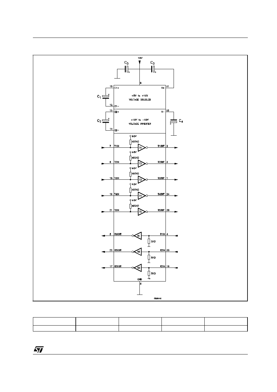
APPLICATION CIRCUITS
CAPACITANCE VALUE (
µ
F)
C1
C2.
C3
C4
C5
0.1
0.1
0.1
0.1
0.1