 | ÐлекÑÑоннÑй компоненÑ: ST22FJ1M | СкаÑаÑÑ:  PDF PDF  ZIP ZIP |
Äîêóìåíòàöèÿ è îïèñàíèÿ www.docs.chipfind.ru
1/8
DATA BRIEF
December 2003
This is Brief Data from STMicroelectronics. Details are subject to change without notice. For complete data, please contact
your nearest Sales Office or SmartCard Products Divison, Rousset, France. Fax: (+33) 4 42 68 87 29.
ST22FJ1M
Smartcard 32-Bit RISC MCU with 1 Mbytes
FLASH & JavacardTM HW Execution
PRODUCT FEATURES
I
32-BIT RISC CPU WITH 24-BIT LINEAR
MEMORY ADDRESSING
I
768 KBYTES USER FLASH
I
16 KBYTES USER RAM
I
16 KBYTES USER SECONDARY RAM
I
256 KBYTES USER PAGE-FLASH
32-BIT RISC CPU
I
DUAL INSTRUCTION SET, JAVACARDTM
AND NATIVE
I
4-STAGE PIPELINE
I
16 GENERAL PURPOSE 32-BIT REGISTERS,
AND 11 SPECIAL REGISTERS
I
4 MASKABLE INTERRUPT LEVELS
I
SUPERVISOR AND USER MODES
SECURITY
I
CPU SECURITY INSTRUCTIONS
DES and 3DES instructions
Fast Multiply and Accumulate instructions for
Public Key and Elliptic Curve Cryptography
I
CPU DPA/SPA COUNTERMEASURES
I
RANDOM NUMBER GENERATOR
I
HARDWARE RAM DESTRUCTION
I
CLOCK AND POWER MANAGEMENT
I
VOLTAGE AND CLOCK FREQUENCY
SENSORS
I
ADVANCED MEMORY PROTECTION
Memory Protection Unit for application
firewalling and peripheral access control
Domain switching securely controlled by
protected Context Stack
Native/Java, Code/Data memory attributes
with 256-byte granularity for Page-Flash, and
8-Kbyte granularity for Flash and ROM
Each FLASH sector can be independently set
as read-only
I
FOUR WORKING STACKS
Java stack with both 16 and 32-bit accesses
User and Supervisor mode stacks
Security Context stack
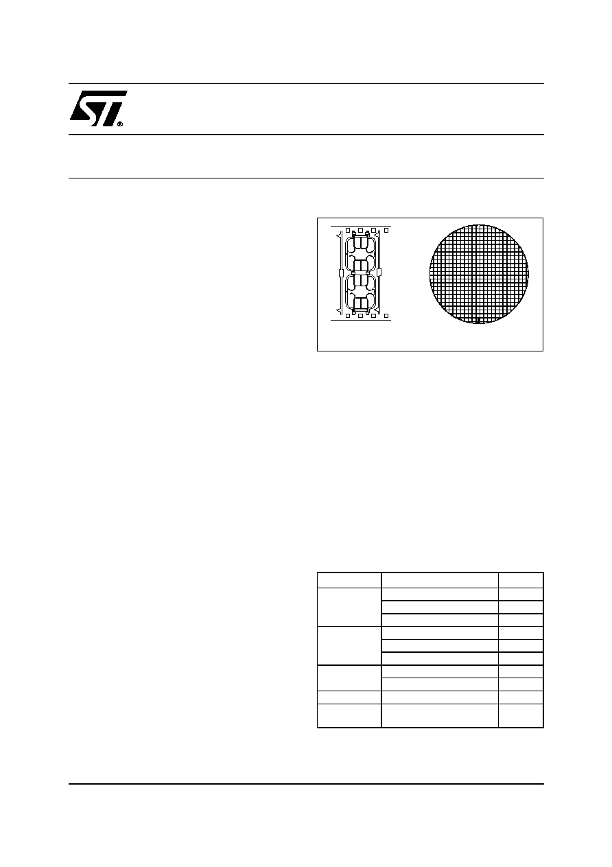
Figure 1. Delivery Form
CRYPTOGRAPHIC LIBRARY
I
ASYMMETRICAL ALGORITHMS
Software Crypto libraries in separate ROM
area for efficient algorithm coding using a set
of advanced functions. RSA, signature/
verification
RSA key calculation including Prime number
generation SHA-1
I
SYMMETRICAL ALGORITHMS
DES, Triple DES, AES
CRYPTOGRAPHY PERFORMANCE
The following table provides the cryptographic
performances of the ST22FJ1M based on ST
Crypto Library.
Table 1. Preliminary Cryptographic
Performances
Note: 1) Internal clock at 33 MHz
Note: 2) CRT: Chinese Reminder Theorem
Algorithm
Function
Time
1)
RSA
1024 bits
Signature with CRT
79.0 ms
Signature without CRT
2)
242.0 ms
Verification (e=0x10001)
3.6 ms
RSA
2048 bits
Signature with CRT
485.0 ms
Signature without CRT
1.7 s
Verification (e=0x10001)
11.0 ms
DES
Triple
18 µs
Single
8 µs
SHA-1
512-bit Block
194 µs
AES-128
Encryption including subkey
computation
85 µs
4
4
4
4
Micromodule
Wafer

ST22FJ1M
2/8
MEMORY
I
HIGHLY RELIABLE CMOS
FLASHTECHNOLOGY
10 years data retention, 100,000 Erase/Write
cycles endurance
64 Kbytes sector Erase in 1.5 s typical
32-bit word program in 100 µs for FLASH
Div 2 jittsi update and 200 µs for Page-Flash
typical in User mode
I
HIGHLY RELIABLE CMOS PAGE-FLASH
TECHNOLOGY
10 years data retention, 100,000 Erase/Write
cycles endurance
32-bit word Erase in 2 ms typical
2K byte sector erase in 50 ms typical
32-bit word program in 30 µs typical in User
mode, 10 µs in Issuer mode
I
FAST AND SECURE FLASH LOADER
I
HIGH PERFORMANCE MEMORY
Dual memory buses for data and instruction
Byte, Short (2) and Word (4) load and store
Address auto-increment
OTHER FEATURES
I
HARDWARE ASYNCHRONOUS SERIAL
INTERFACE (ASI)
1M baud rate capability
2 serial I/O ports compatible ISO 7816-3 T=0
and T=1
I
2 USER CONFIGURABLE 12-BIT AND 16-BIT
TIMERS WITH INTERRUPT
I
CENTRAL INTERRUPT CONTROLLER WITH
UP TO 16 INPUT LINES
I
UP TO 8 MHZ BIG JITTER DIV 4
I
EXTERNAL CLOCK FROM 1 MHz TO 10 MHz
I
3 V TO 5.5 V SUPPLY VOLTAGE
I
TEMPERATURE RANGE -25° C to +85° C
I
POWER SAVING STANDBY MODE
I
ESD PROTECTION GREATER THAN 4000 V
I
UNIQUE IDENTIFICATION PER DIE
3/8
ST22FJ1M
DESCRIPTION
The ST22FJ1M is a member of the SmartJTM plat-
form using a 32-bit Reduced Instruction Set Com-
puter (RISC) core to execute both Native RISC
instructions and JavaCardTM 2.x Technology in-
struction (byte codes) directly.
Direct JavaCardTM byte code execution provides
high performance advantage over processors that
emulate the JavaCardTM byte code instruction set.
The product features a 24-bit wide linear ad-
dressing capability and includes 768 Kbytes of
User Flash, 16 KBytes of User RAM, 16 Kbytes
of User secondary RAM, and 256 KBytes of
User Page-Flash.
The Flash memory is organized in 12 sectors of
64 Kbytes each, with 8 Kbytes sub-sectors.
Each sector can be erased in 1.5 s typical. All
32-bit words are programmed in 100 µs typical
in User mode.
One of the Flash sector is reserved by the HSI
for saving data, when modifying a sector.
The Page-Flash memory is organized in 128
sub-sectors of 2 Kbytes each. Each sub-sector
can be erased in 50 ms typical. All 32-bit words
are programmed in 200 µs typical in User mode.
The secondary RAM memory can be used as a
regular RAM, or dynamically mapped to the ad-
dress of any of the 96 Flash sub-sectors, or
mapped to two consecutive Flash sub-sectors.
This memory can be used to speed-up process-
ing and decrease power consumption.
The product includes a fast and secure Flash
loader. The OS code is received from the OS
manufacturer in an encrypted form, and
decrypted on-chip before programming the
Flash.
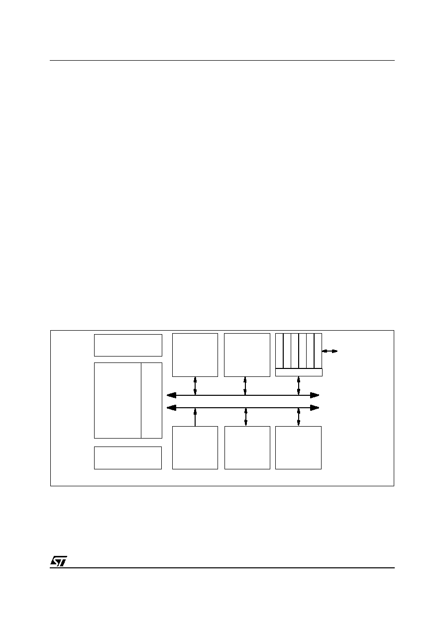
Memory and Peripheral accesses are controlled
by a Memory Protection Unit that allows to imple-
ment firewalls between applications.
Memories are accessed via two different buses,
allowing simultaneous accesses to code and data.
Memory load and stores can be performed at byte,
short (2-bytes), or word (4-bytes) granularity, with
optional pointer auto increment.
The ST22 core includes dedicated DES instruc-
tions for Secret Key cryptography, a fast Multiply
and Accumulate instruction for Public Key cryptog-
raphy (RSA) and Elliptic Curve cryptography. The
ST22 core also includes specific instructions for
security.
The product has clock and power management, 2
User configurable Timers, a Central Interrupt Con-
troller and a Random Number Generator.
Figure 2. SmartJTM Platform FLASH Architecture
ST ROM
FLASH
RAM
PERIPHERALS
BUS 2
BUS 1
TI
M
E
R
AS
I
....
POWER MNGT.
CLOCK MNGT.
ISO
7816
S
E
CUR
I
T
Y
RN
G
...
.
....
SCP 160b/PRZ
32-bit
RISC
CORE
MP
U
P-FLASH
SECONDARY
RAM

ST22FJ1M
4/8
The product has two execution modes. Java mode
is used when JavaCardTM 2.x byte codes are be-
ing executed. Native mode is used for long JavaC-
ardTM byte codes, Native methods and system
routines. The processor enters Java mode when a
dispatch (DISP) instruction is encountered. When
executing in Native mode, there are two privilege
levels, User and Supervisor. Some instructions
can only be executed in Supervisor mode.
Instructions are of variable length, from 1 to 4
bytes in Native mode.
Special instructions exist for single-cycle stack op-
erations, a frequent occurrence in Java code.
Short branches and conditional branches within a
1 KByte block or the entire 16-MByte instruction
space are supported.
The product has four stages of pipeline in Native
mode: fetch, decode, execute and write-back. In
Java mode, there are five stages of pipeline: byte
code-fetch, byte code-decode, decode, execute
and write-back.
The CPU core has 16 32-bit general purpose reg-
isters, as well as 11 special registers of variable
length.
The chip also features a very high performance
Asynchronous Serial Interface (ASI) to support
high speed serial communication protocols com-
patible with ISO 7816 standards.
It is manufactured using the highly reliable ST
CMOS FLASH technology.
EMBEDDED SOFTWARE
The Hardware Software Interface (HSI) imple-
ments the Hardware abstraction layer. It consists
of C interfaces to the FLASH memory and periph-
erals. The drivers are:
Non Volatile Memory
Flash memory
Asynchronous Serial Interface
Central Interrupt Controller
Timer
Random Number Generator
Clock Manager
Memory Protection Unit
Sensors
Security
Note:
The HSI driver software layer is access to the
peripherals and Non Volatile Memory for
programming or erasing.
Only the OS and JavaCardTM Virtual Machine
(JVM) domains can access the HSI software
layer (In the following the term OS will refer to
the software layer that is directly interfaced to
the HSI).
CRYPTOGRAPHIC LIBRARY
ST proposes a complete set of firmware subrou-
tines. This library is located in a specific ROM ar-
ea. It saves the operating system designer from
coding first layer functions and allows him to con-
centrate on algorithms, Public Key Cryptography
and Secret Key Cryptography protocols imple-
mentation.
The cryptographic library, located in a specific
ROM area, contains firmware functions for:
I
ASYMMETRICAL ALGORITHMS:
basic mathematics including modular
squaring and multiplication for various
lengths;
modular exponentionation;
more elaborate functions such as RSA
signatures and verifications for modulo length
up to 2048 bits long;
full internal key generation for signatures/
verifications. This guarantees that the secret
key will never be known outside the chip and
contributes to the overall system security.
long random number generation
SHA-1
RSA key generation
I
SYMMETRICAL ALGORITHMS
DES, Triple DES
AES-128, AES-192, AES-256
5/8
ST22FJ1M
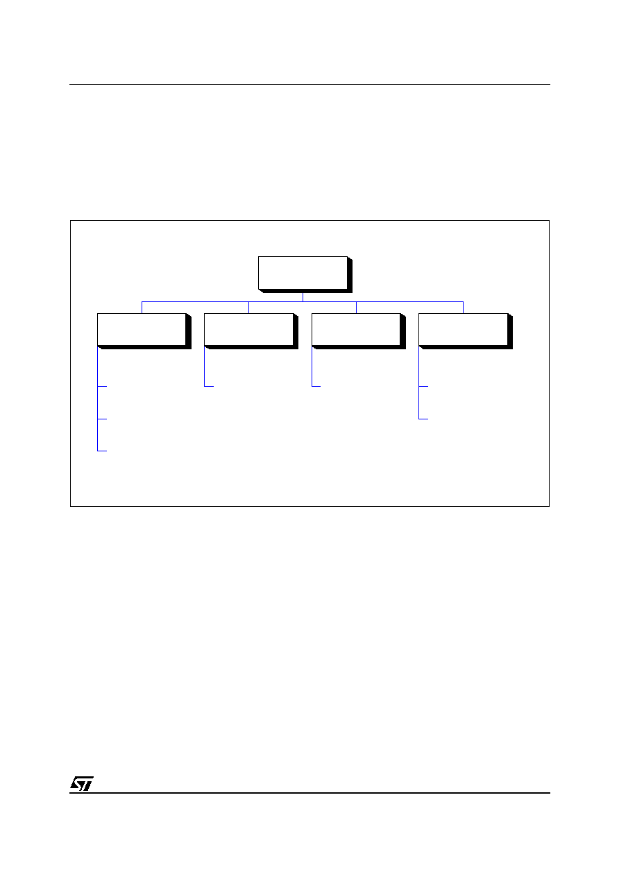
SOFTWARE DEVELOPMENT ENVIRONMENT
Modularity, flexibility and methodology are the key
words for the SmartJTM Development Tools Plat-
form. Using the same interface, the developers are
able to create, compile and debug a project.
The SmartJTM Integrated Development environ-
ment (IDE) includes:
A code Generation chain: C/C++ compiler,
assembler and linker. The assembler supports
both native and JavaCardTM instruction sets.
An instruction set simulator, a cycle accurate
simulator, a C/C++ source level debugger.
Figure 3. SmartJTM Platform Concept
Note: 1) SmartJTM Platform Technology License Agreement required
Note: 2) SmartJTM Technology License and Distribution Agreement required
SmartJ Platform
ST22 Core Plus
ROM RAM NVM
Size Definition
STD PERIPHERALS
& SECURITY
ASI, Timers, Security
Mechanisms,...
CUSTOMS PLUGS-IN (1)
SmartJ IDE
SmartJ-Tools Pack-CD
SmartJ H/W Development
(not yet available)
VHDL Library (1)
SmartJ
ISO 15408 Certified
Embedded Library
HSI (2)
Memory & Std Peripherals Drivers
CRYPTO (2)
Certified Crypto Library
(DES, 3DES, RSA, SHA, AES...)
484