ST24LC21
1Kb (x8) DUAL MODE SERIAL EEPROM
for VESA Plug&Play
NOT FOR NEW DESIGN
June 1997
1/18
This is information on a product still in production but not recommended for new designs.
1 MILLION ERASE/WRITE CYCLES
40 YEARS DATA RETENTION
2.5V to 5.5V SINGLE SUPPLY VOLTAGE
400k Hz COMPATIBILITY OVER the FULL
RANGE of SUPPLY VOLTAGE
TWO WIRE SERIAL INTERFACE I
2
C BUS
COMPATIBLE
PAGE WRITE (up to 8 BYTES)
BYTE, RANDOM and SEQUENTIAL READ
MODES
SELF TIMED PROGRAMMING CYCLE
AUTOMATIC ADDRESS INCREMENTING
ENHANCED ESD/LATCH UP
PERFORMANCES
ST24LC21 is replaced by the ST24LC21B
DESCRIPTION
The ST24LC21 is a 1K bit electrically erasable
programmable memory (EEPROM), organized by
8 bits.This device can operate in two modes: Trans-
mit Only mode and I
2
C bidirectional mode. When
powered, the device is in Transmit Only mode with
EEPROM data clocked out from the rising edge of
the signal applied on VCLK.
The device will switch to the I
2
C bidirectional mode
upon the falling edge of the signal applied on SCL
pin. The ST24LC21 cannot switch from the I
2
C
bidirectional mode to the Transmit Only mode (ex-
cept when the power supply is removed). The
device operates with a power supply value as low
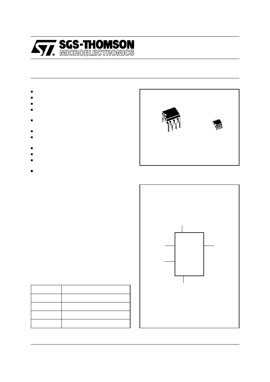
as 2.5V. Both Plastic Dual-in-Line and Plastic Small
Outline packages are available.
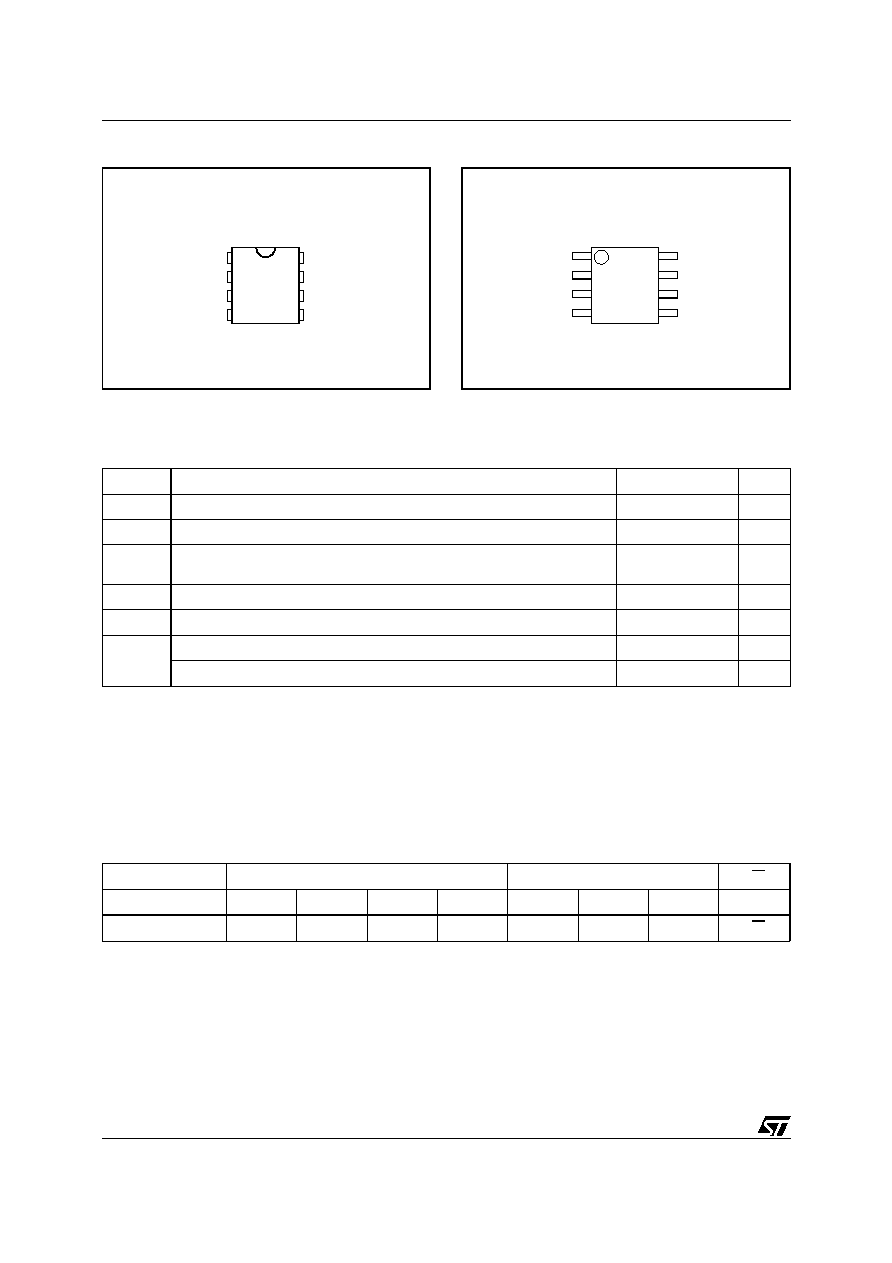
AI01489
SDA
VCC
ST24LC21
VCLK
SCL
VSS
Figure 1. Logic Diagram
SDA
Serial Data Address Input/Output
SCL
Serial Clock (I
2
C mode)
V
CC
Supply Voltage
V
SS
Ground
VCLK
Clock Transmit only mode
Table 1. Signal Names
8
1
SO8 (M)
8
1
PSDIP8 (B)
0.25mm Frame
SDA
VSS
SCL
VCLK
NC
NC
VCC
NC
AI01499
ST24LC21
1
2
3
4
8
7
6
5
Figure 2A. DIP Pin Connections
1
AI01500
2
3
4
8
7
6
5
SDA
VSS
SCL
VCLK
NC
NC
VCC
NC
ST24LC21
Figure 2B. SO Pin Connections
Symbol
Parameter
Value
Unit
T
A
Ambient Operating Temperature
grade 1
0 to 70
�
C
T
STG
Storage Temperature
�65 to 150
�
C
T
LEAD
Lead Temperature, Soldering
(SO8 package)
(PSDIP8 package)
40 sec
10 sec
215
260
�
C
V
IO
Input or Output Voltages
�0.3 to 6.5
V
V
CC
Supply Voltage
�0.3 to 6.5
V
V
ESD
Electrostatic Discharge Voltage (Human Body model)
(2)
4000
V
Electrostatic Discharge Voltage (Machine model)
(3)
500
V
Notes: 1. Except for the rating "Operating Temperature Range", stresses above those listed in the Table "Absolute Maximum Ratings"
may cause permanent damage to the device. These are stress ratings only and operation of the device at these or any other
conditions above those indicated in the Operating sections of this specification is not implied. Exposure to Absolute Maximum
Rating conditions for extended periods may affect device reliability. Refer also to the SGS-THOMSON SURE Program and other
relevant quality documents.
2. MIL-STD-883C, 3015.7 (100pF, 1500
).
3. EIAJ IC-121 (Condition C) (200pF, 0
).
Table 2. Absolute Maximum Ratings
(1)
Device Code
Chip Enable
RW
Bit
b7
b6
b5
b4
b3
b2
b1
b0
Device Select
1
0
1
0
X
X
X
RW
Note: The MSB b7 is sent first.
X = 0 or 1.
Table 3. Device Select Code
Warning: NC = Not Connected
Warning: NC = Not Connected
2/18
ST24LC21
AI01501
Bit 7
VCC
tVPU
SCL
SDA
VCLK
Bit 6
Bit 7
VCC
SCL
SDA
VCLK
Bit 6
Bit 6
Bit 4
Bit 0
1
2
8
9
10
11
12
13
17
18
19
20
Bit 5
Figure 3. Transmit Only Mode Waveforms
Mode
RW bit
VCLK
Bytes
Initial Sequence
Current Address Read
'1'
X
1
START, Device Select, RW = '1'
Random Address Read
'0'
X
1
START, Device Select, RW = '0', Address,
'1'
X
reSTART, Device Select, RW = '1'
Sequential Read
'1'
X
1 to 128
Similar to Current or Random Mode
Byte Write
'0'
V
IH
1
START, Device Select, RW = '0'
Page Write
'0'
V
IH
8
START, Device Select, RW = '0'
Note: X = V
IH
or V
IL
Table 4. Operating Modes
3/18
ST24LC21
Transmit Only Mode
After a Power-up, the device is in the Transmit Only
mode. A proper initialization sequence must supply
nine clock pulses on the VCLK pin (in order to
internally synchronize the device). During this in-
itialization sequence, the SDA pin is in high imped-
ance. On the rising edge of the tenth pulse applied
on VCLK pin, the device will output the first bit of
byte located at address 00h (most significant bit
first).
A byte is clocked out (on SDA pin) with nine clock
pulses on VCLK: 8 clock pulses for the data byte
and one extra clock pulse for a Don't Care bit.
As long as the SCL pin is held high, each byte of
the memory array is transmitted serially on the SDA
pin with an automatic address increment.
When the last byte is transmitted, the address
counter will roll-over to location 00h.
I
2
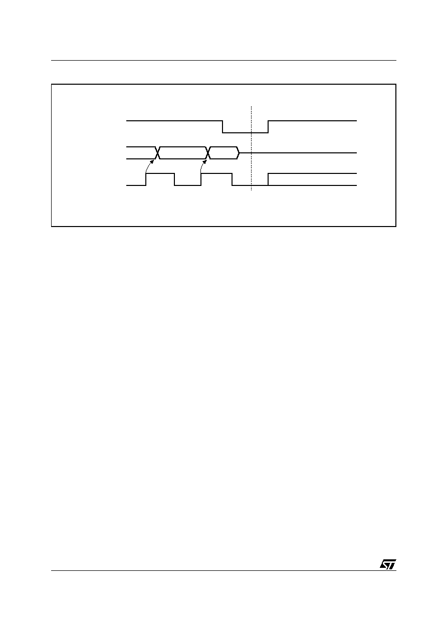
C Bidirectional Mode
The device can be switched from Transmit Only
mode to I
2
C Bidirectional mode by applying a valid
high to low transition on the SCL pin (see Figure 4).
When the device is in the I2C Bidirectional mode,
the VCLK input enables (or inhibits) the execution
of any write instruction: if VCLK = 1, write instruc-
tions are executed; if VCLK = 0, write instructions
are not executed.
The device is compatible with the I
2
C standard, two
wire serial interface which uses a bi-directional data
bus and serial clock. The device carries a built-in 4
bit, unique device identification code (1010) corre-
sponding to the I
2
C bus definition.
The device behaves as a slave device in the I
2
C
protocol with all memory operations synchronized
by the serial clock. Read and write operations are
initiated by a START condition generated by the
bus master. The START condition is followed by a
stream of 7 bits (identification code 1010XXX), plus
one read/write bit and terminated by an acknow-
ledge bit.
When writing data to the memory it responds to the
8 bits received by asserting an acknowledge bit
during the 9th bit time. When data is read by the
bus master, it acknowledges the receipt of the data
bytes in the same way. Data transfers are termi-
nated with a STOP condition.
Power On Reset: V
CC
lock out write protect. In
order to prevent data corruption and inadvertent
write operations during power up, a Power On
Reset (POR) circuit is implemented. Until the V
CC
voltage has reached the POR threshold value, the
internal reset is active, all operations are disabled
and the device will not respond to any command.
In the same way, when V
CC
drops down from the
operating voltage to below the POR threshold
value, all operations are disabled and the device
will not respond to any command. A stable V
CC
must be applied before applying any logic signal.
AI01502
SCL
SDA
VCLK
Bi-Directional Mode
Transmit Only Mode
Figure 4. Transition Mode Waveforms
4/18
ST24LC21
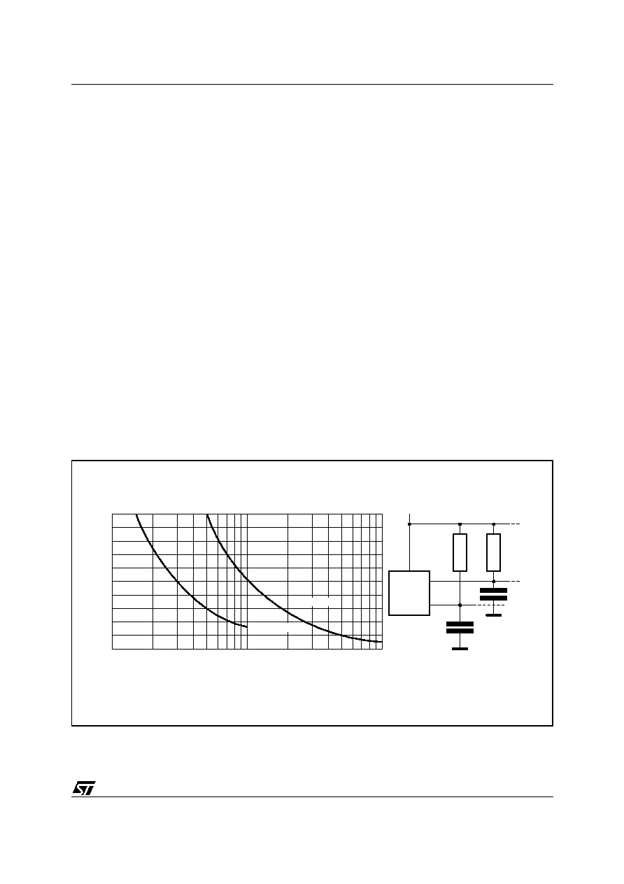
AI01665
VCC
CBUS
SDA
RL
MASTER
RL
SCL
CBUS
100
0
4
8
12
16
20
CBUS (pF)
Maximum RP value (k
)
10
1000
fc = 400kHz
fc = 100kHz
Figure 5. Maximum R
L
Value versus Bus Capacitance (C
BUS
) for an I
2
C Bus
SIGNAL DESCRIPTIONS
I
2
C Serial Clock (SCL). The SCL input pin is used
to synchronize all data in and out of the memory. A
resistor can be connected from the SCL line to V
CC
to act as a pull up (see Figure 5).
Transmit Only Clock (VCLK). The VCLK input pin
is used to synchronize data out when the
ST24LC21 is in Transmit Only mode. The VCLK
input offers also a Write Enable (active high) func-
tion when the ST24LC21 is in I
2
C bidirectional
mode.
Serial Data (SDA). The SDA pin is bi-directional
and is used to transfer data in or out of the memory.
It is an open drain output that may be wire-OR'ed
with other open drain or open collector signals on
the bus. A resistor must be connected from the SDA
bus line to V
CC
to act as pull up (see Figure 5).
DEVICE OPERATION
I
2
C Bus Background
The ST24LC21 supports the I
2
C protocol. This
protocol defines any device that sends data onto
the bus as a transmitter and any device that reads
the data as a receiver. The device that controls the
data transfer is known as the master and the other
as the slave. The master will always initiate a data
transfer and will provide the serial clock for syn-
chronisation. The ST24LC21 are always slave de-
vices in all communications.
Start Condition. START is identified by a high to
low transition of the SDA line while the clock SCL
is stable in the high state. A START condition must
precede any command for data transfer. Except
during a programming cycle, the ST24LC21 con-
tinuously monitor the SDA and SCL signals for a
START condition and will not respond unless one
is given.
Stop Condition. STOP is identified by a low to high
transition of the SDA line while the clock SCL is
stable in the high state. A STOP condition termi-
nates communication between the ST24LC21 and
the bus master. A STOP condition at the end of a
Read command forces the standby state. A STOP
condition at the end of a Write command triggers
the internal EEPROM write cycle.
Acknowledge Bit (ACK). An acknowledge signal
is used to indicate a successfull data transfer. The
bus transmitter, either master or slave, will release
the SDA bus after sending 8 bits of data. During the
9th clock pulse period the receiver pulls the SDA
bus low to acknowledge the receipt of the 8 bits of
data.
5/18
ST24LC21