 | –≠–ª–µ–∫—Ç—Ä–æ–Ω–Ω—ã–π –∫–æ–º–ø–æ–Ω–µ–Ω—Ç: ST3232B | –°–∫–∞—á–∞—Ç—å:  PDF PDF  ZIP ZIP |
1/11
May 2002
s
300
µ
A SUPPLY CURRENT
s
300Kbps MINIMUM GUARENTEED DATA
RATE
s
6V/
µ
s MINIMUM GUARANTEED SLEW RATE
s
MEET EIA/TIA-232 SPECIFICATIONS DOWN
TO 3V
s
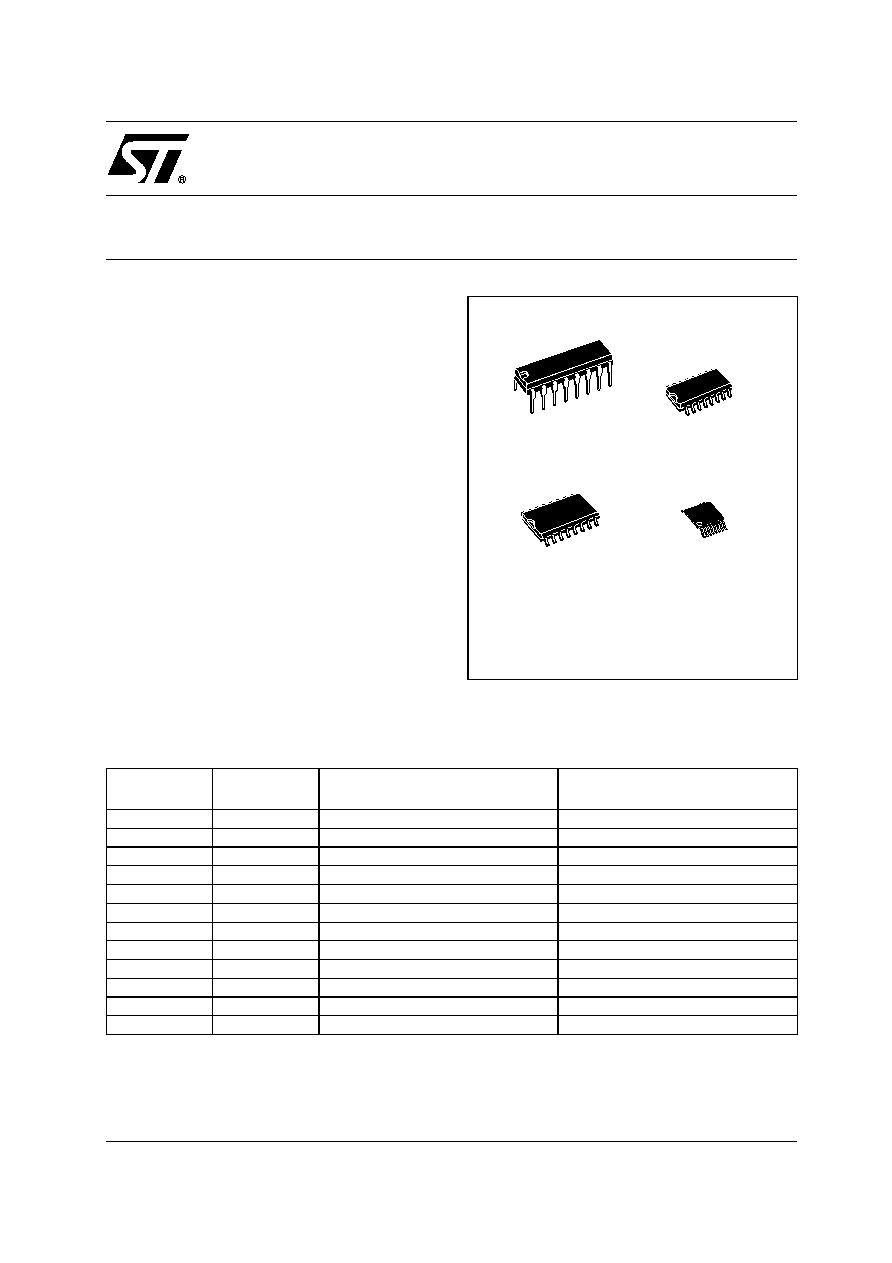
AVAILABLE IN DIP-16, SO-16, SO-16 LARGE
AND TSSOP16
DESCRIPTION
The ST3232 is a 3V powered EIA/TIA-232 and
V.28/V.24 communication interface with low
power requirements, high data-rate capabilities.
ST3232 has a proprietary low dropout transmitter
output stage providing true RS-232 performance
from 3 to 5.5V supplies. The device requires only
four small 0.1
µ
F standard external capacitors for
operations from 3V supply.
The ST3232 has two receivers and two drivers.
The device is guaranteed to run at data rates of
250Kbps while maintaining RS-232 output levels.
Typical applications are Notebook, Subnotebook
and Palmtop Computers, Battery Powered
Equipment, Hand-Held Equipment, Peripherals
and Printers.
ORDERING CODES
Type
Temperature
Range
Package
Comments
ST3232CN
0 to 70 ∞C
DIP-16
25parts per tube / 40tube per box
ST3232BN
-40 to 85 ∞C
DIP-16
25parts per tube / 40tube per box
ST3232CD
0 to 70 ∞C
SO-16 (Tube)
50parts per tube / 20tube per box
ST3232BD
-40 to 85 ∞C
SO-16 (Tube)
50parts per tube / 20tube per box
ST3232CDR
0 to 70 ∞C
SO-16 (Tape & Reel)
2500 parts per reel
ST3232BDR
-40 to 85 ∞C
SO-16 (Tape & Reel)
2500 parts per reel
ST3232CW
0 to 70 ∞C
SO-16 Large (Tube)
49parts per tube / 25tube per box
ST3232BW
-40 to 85 ∞C
SO-16 Large (Tube)
49parts per tube / 25tube per box
ST3232CWR
0 to 70 ∞C
SO-16 Large (Tape & Reel)
1000 parts per reel
ST3232BWR
-40 to 85 ∞C
SO-16 Large (Tape & Reel)
1000 parts per reel
ST3232CTR
0 to 70 ∞C
TSSOP16 (Tape & Reel)
2500 parts per reel
ST3232BTR
-40 to 85 ∞C
TSSOP16 (Tape & Reel)
2500 parts per reel
ST3232
3 TO 5.5V, LOW POWER, UP TO 400KBPS,
RS-232 DRIVERS AND RECEIVERS
SOP Large
DIP
SOP
TSSOP

ST3232
2/11
PIN CONFIGURATION
PIN DESCRIPTION
ABSOLUTE MAXIMUM RATINGS
Absolute Maximum Ratings are those values beyond which damage to the device may occur. Functional operation under these condition is
not implied. V+ and V- can have a maximum magnitude of +7V, but their absolute addition can not exceed 13 V.
PlN N∞
SYMBOL
NAME AND FUNCTION
1
C
1
+
Positive Terminal for the first Charge Pump Capacitor
2
V+
Doubled Voltage Terminal
3
C
1
-
Negative Terminal for the first Charge Pump Capacitor
4
C
2
+
Positive Terminal for the second Charge Pump Capacitor
5
C
2
-
Negative Terminal for the second Charge Pump Capacitor
6
V-
Inverted Voltage Terminal
7
T2
OUT
Second Transmitter Output Voltage
8
R2
IN
Second Receiver Input Voltage
9
R2
OUT
Second Receiver Output Voltage
10
T2
IN
Second Transmitter Input Voltage
11
T1
IN
First Transmitter Input Voltage
12
R1
OUT
First Receiver Output Voltage
13
R1
IN
First Receiver Input Voltage
14
T1
OUT
First Transmitter Output Voltage
15
GND
Ground
16
V
CC
Supply Voltage
Symbol
Parameter
Value
Unit
V
CC
Supply Voltage
-0.3 to 6
V
V+
Doubled Voltage Terminal
(V
CC
- 0.3) to 7
V
V-
Inverted Voltage Terminal
0.3 to -7
V
V+ +|V-|
13
V
T
IN
Transmitter Input Voltage Range
-0.3 to 6
V
R
IN
Receiver Input Voltage Range
±
25
V
T
OUT
Transmitter Output Voltage Range
±
13.2
V
R
OUT
Receiver Output Voltage Range
-0.3 to (V
CC
+ 0.3)
V
t
SHORT
Transmitter Output Short to GND Time
Continuous
ST3232
3/11
ELECTRICAL CHARACTERISTICS
(C
1
- C
4
= 0.1
µ
F, V
CC
= 3V to 5.5V, T
A
= -40 to 85∞C, unless otherwise specified.
Typical values are referred to T
A
= 25∞C)
LOGIC INPUT ELECTRICAL CHARACTERISTICS
(C
1
- C
4
= 0.1
µ
F, V
CC
= 3V to 5.5V, T
A
= -40 to 85∞C, unless otherwise specified.
Typical values are referred to T
A
= 25∞C)
Note 1: Transmitter input hysteresis is typically 250mV
TRANSMITTER ELECTRICAL CHARACTERISTICS
(C
1
- C
4
= 0.1
µ
F tested at V
CC
= 3V to 5.5V, T
A
= -40 to 85∞C, unless otherwise specified.
Typical values are referred to T
A
= 25∞C)
RECEIVER ELECTRICAL CHARACTERISTICS
(C
1
- C
4
= 0.1
µ
F tested at V
CC
= 3V to 5.5V, T
A
= -40 to 85∞C, unless otherwise specified.
Typical values are referred to T
A
= 25∞C)
Symbol
Parameter
Test Conditions
Min.
Typ.
Max.
Unit
I
SUPPLY
V
CC
Power Supply Current
No Load V
CC
= 3V ±10% T
A
= 25∞C
0.3
1
mA
No Load V
CC
= 5V ±10% T
A
= 25∞C
1
2
mA
Symbol
Parameter
Test Conditions
Min.
Typ.
Max.
Unit
V
TIL
Input Logic Threshold Low
T-IN (Note 1)
0.8
V
V
TIH
Input Logic Threshold High
V
CC
= 3.3V
V
CC
= 5V
2
2.4
V
V
I
IL
Input Leakage Current
T-IN
±
0.01
±
1
µ
A
Symbol
Parameter
Test Conditions
Min.
Typ.
Max.
Unit
V
TOUT
Output Voltage Swing
All Transmitter outputs are loaded with
3K
to GND
±
5
±
5.4
V
R
TOUT
Transmitter Output
Resistance
V
CC
= V+ = V- = 0V
V
OUT
=
±
2V
300
10M
I
TSC
Output Short Circuit
Current
V
CC
= 3V to 5V
V
OUT
=
±
12V
±
60
mA
Symbol
Parameter
Test Conditions
Min.
Typ.
Max.
Unit
V
RIN
Receiver Input Voltage
Operating Range
-25
25
V
V
RIL
RS-232 Input Threshold
Low
T
A
= 25∞C
V
CC
= 3.3V
T
A
= 25∞C
V
CC
= 5V
0.6
0.8
1.2
1.5
V
V
V
RIH
RS-232 Input Threshold
High
T
A
= 25∞C
V
CC
= 3.3V
T
A
= 25∞C
V
CC
= 5V
1.5
1.8
2.4
2.4
V
V
V
RIHYS
Input Hysteresis
0.3
V
R
RIN
Input Resistance
T
A
= 25∞C
3
5
7
K
V
ROL
TTL/CMOS Output Voltage
Low
I
OUT
= 1.6mA
0.4
V
V
ROH
TTL/CMOS Output Voltage
High
I
OUT
= -1mA
V
CC
-0.6 V
CC
-0.1
V
ST3232
4/11
TIMING CHARACTERISTICS
(C
1
- C
4
= 0.1
µ
F, V
CC
= 3V to 5.5V, T
A
= -40 to 85∞C, unless otherwise specified.
Typical values are referred to T
A
= 25∞C)
Transmitter Skew is measured at the transmitter zero cross points
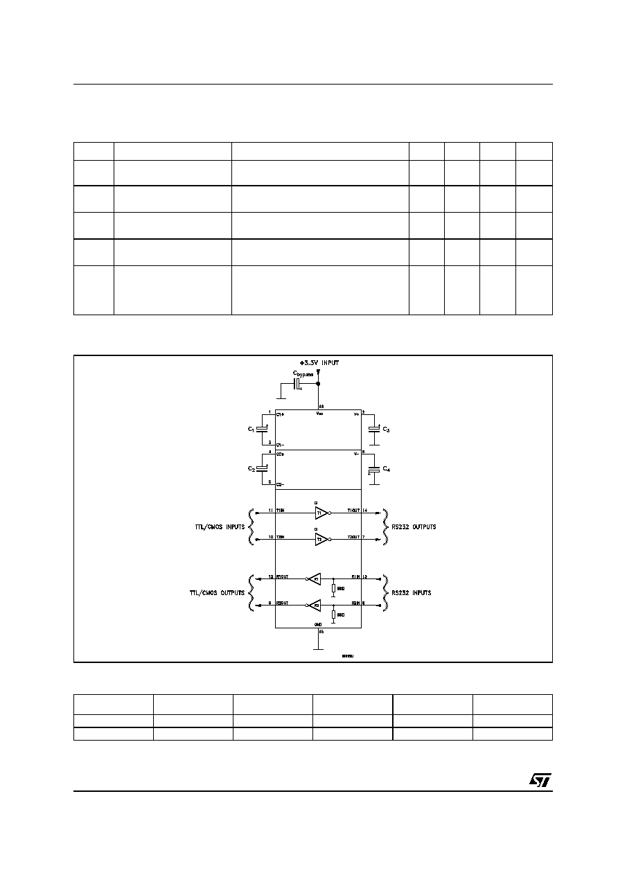
APPLICATION CIRCUITS
CAPACITANCE VALUE (
µ
F)
Symbol
Parameter
Test Conditions
Min.
Typ.
Max.
Unit
D
R
Data Transfer Rate
R
L
= 3K
C
L2
= 1000pF
one trasmitter switching
300
400
Kbps
t
PHLR
t
PLHR
Propagation Delay Input to
Output
R
XIN
= R
XOUT
C
L
= 150pF
0.2
µ
s
|t
PHLT
- t
THL
|
Transmitter Propagation
Delay Difference
(Note 1)
100
ns
|t
PHLR
- t
THR
|
Receiver Propagation Delay
Difference
50
ns
S
RT
Trnasition Slew Rate
T
A
= 25∞C R
L
= 3K
to 7K
V
CC
= 3.3V
measured from +3V to -3V or -3V to +3V
C
L
= 150pF to 1000pF
C
L
= 150pF to 2500pF
6
4
30
30
V/
µ
s
V/
µ
s
V
CC
C1
C2
C3
C4
Cbypass
3.0 to 3.6
0.1
0.1
0.1
0.1
0.1
4.5 to 5.5
0.047
0.33
0.33
0.33
0.33

ST3232
5/11
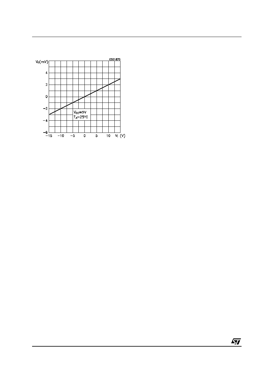
TYPICAL PERFORMANCE CHARACTERISTICS (unless otherwise specified T
j
= 25∞C)
Figure 1 : Driver Voltage Transfer Characteristics
for Trasmitter Inputs
Figure 2 : Driver Voltage Transfer Characteristics
for Receiver Inputs
Figure 3 : Output Current vs Output Low Voltage
Figure 4 : Output Current vs Output Low Voltage
Figure 5 : Output Current vs Output High Voltage
Figure 6 : Output Current vs Output High Voltage
ST3232
6/11
Figure 7 : Receiver Input Resistance
ST3232
7/11
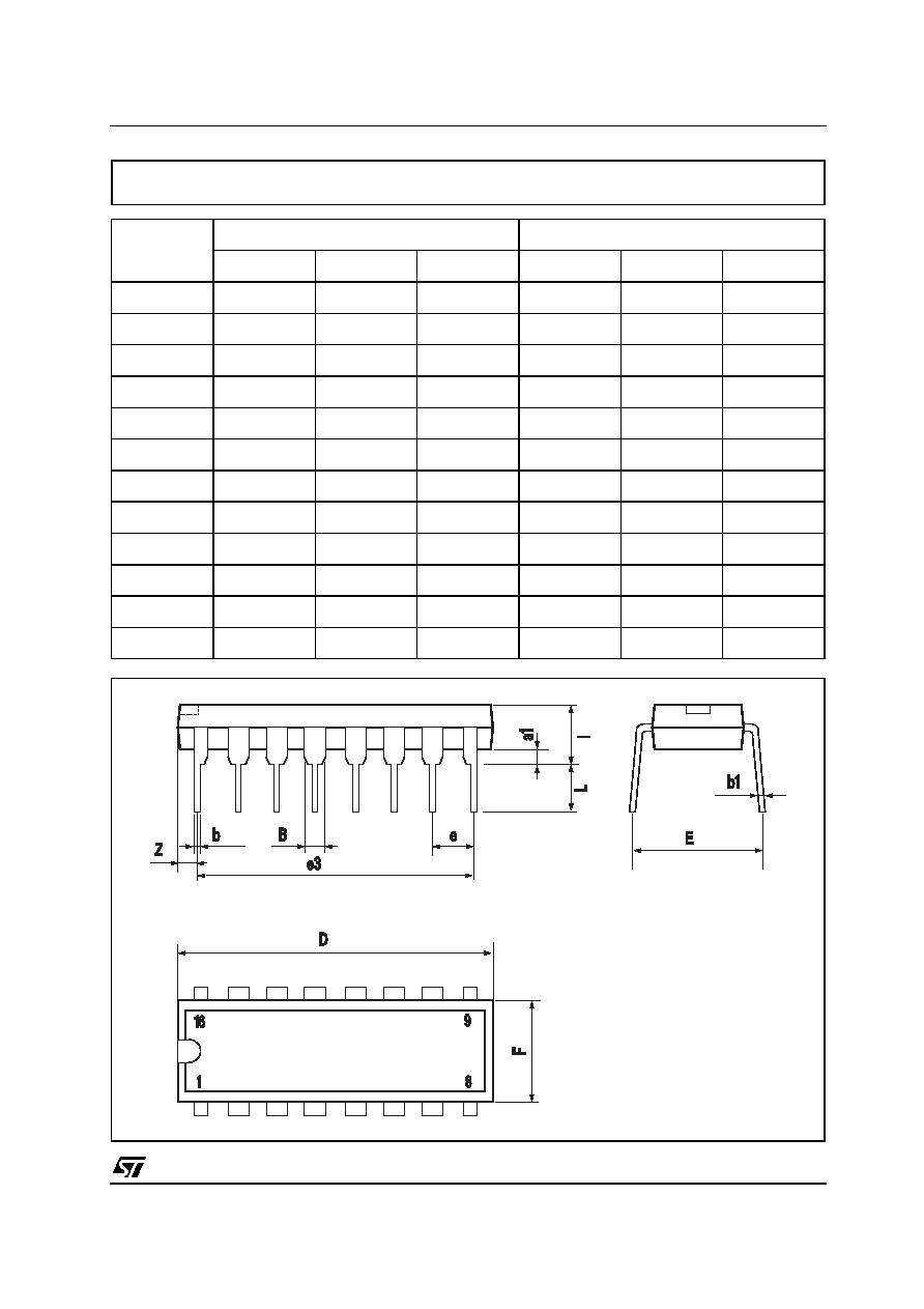
DIM.
mm.
inch
MIN.
TYP
MAX.
MIN.
TYP.
MAX.
a1
0.51
0.020
B
0.77
1.65
0.030
0.065
b
0.5
0.020
b1
0.25
0.010
D
20
0.787
E
8.5
0.335
e
2.54
0.100
e3
17.78
0.700
F
7.1
0.280
I
5.1
0.201
L
3.3
0.130
Z
1.27
0.050
Plastic DIP-16 (0.25) MECHANICAL DATA
P001C
ST3232
8/11
DIM.
mm.
inch
MIN.
TYP
MAX.
MIN.
TYP.
MAX.
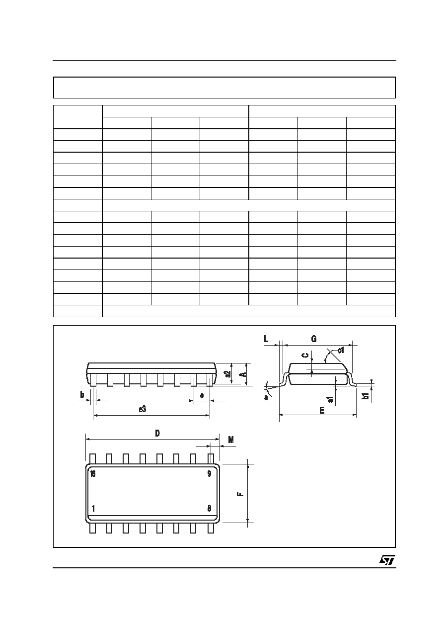
A
1.75
0.068
a1
0.1
0.2
0.003
0.007
a2
1.65
0.064
b
0.35
0.46
0.013
0.018
b1
0.19
0.25
0.007
0.010
C
0.5
0.019
c1
45∞ (typ.)
D
9.8
10
0.385
0.393
E
5.8
6.2
0.228
0.244
e
1.27
0.050
e3
8.89
0.350
F
3.8
4.0
0.149
0.157
G
4.6
5.3
0.181
0.208
L
0.5
1.27
0.019
0.050
M
0.62
0.024
S
8∞ (max.)
SO-16 MECHANICAL DATA
PO13H
ST3232
9/11
DIM.
mm.
inch
MIN.
TYP
MAX.
MIN.
TYP.
MAX.
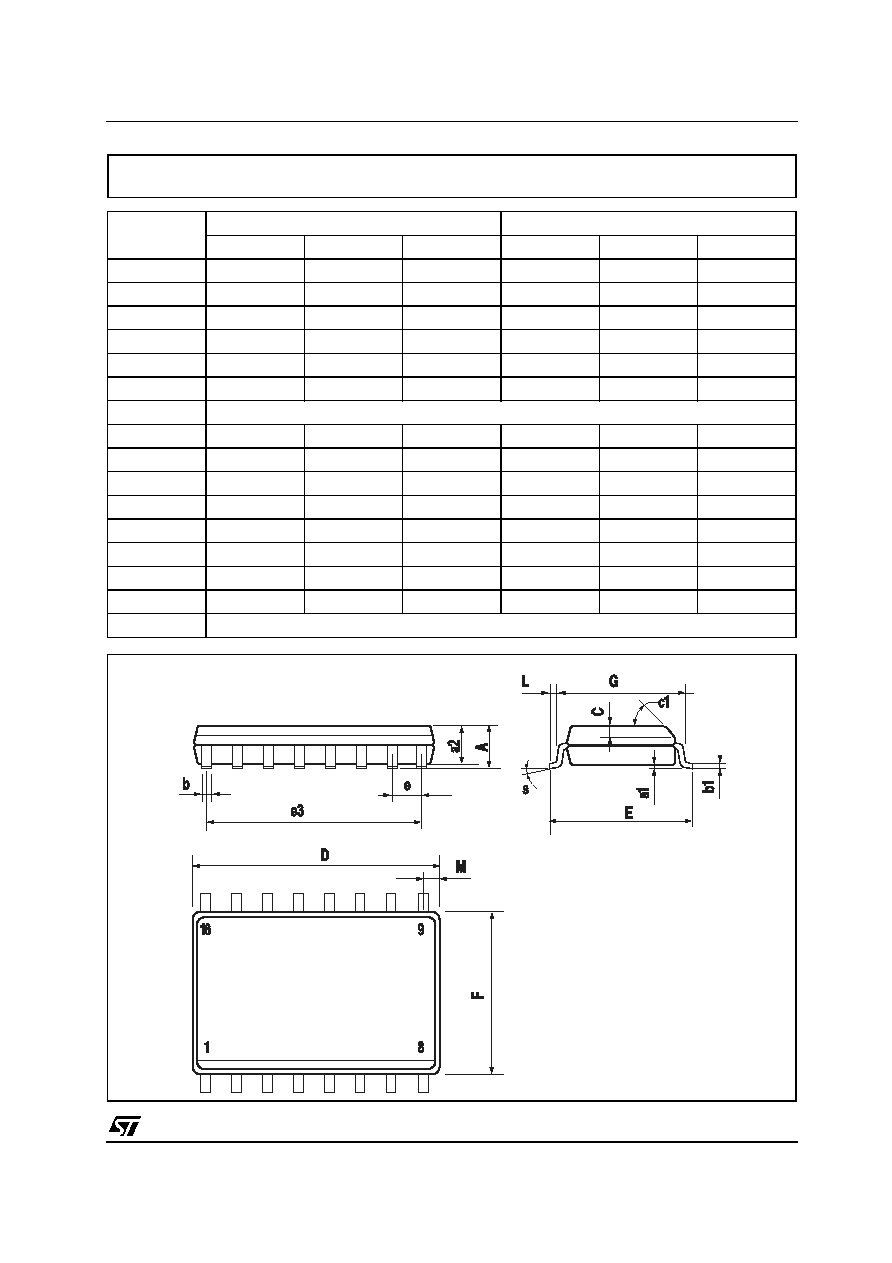
A
2.65
0.104
a1
0.1
0.2
0.004
0.008
a2
2.45
0.096
b
0.35
0.49
0.014
0.019
b1
0.23
0.32
0.009
0.012
C
0.5
0.020
c1
45∞ (typ.)
D
10.1
10.5
0.397
0.413
E
10.0
10.65
0.393
0.419
e
1.27
0.050
e3
8.89
0.350
F
7.4
7.6
0.291
0.300
G
L
0.5
1.27
0.020
0.050
M
0.75
0.029
S
8∞ (max.)
SO-16L MECHANICAL DATA
PO13I
ST3232
10/11
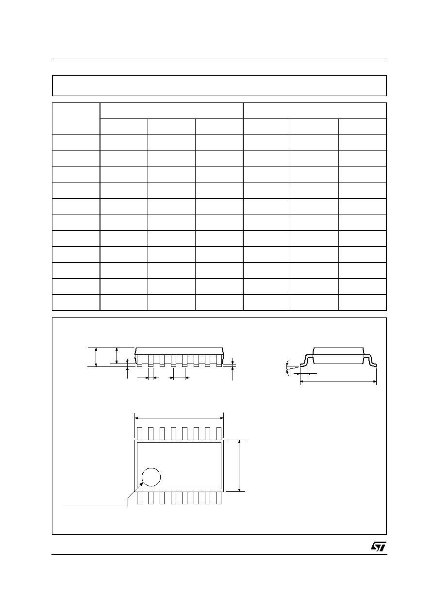
DIM.
mm.
inch
MIN.
TYP
MAX.
MIN.
TYP.
MAX.
A
1.2
0.047
A1
0.05
0.15
0.002
0.004
0.006
A2
0.8
1
1.05
0.031
0.039
0.041
b
0.19
0.30
0.007
0.012
c
0.09
0.20
0.004
0.0089
D
4.9
5
5.1
0.193
0.197
0.201
E
6.2
6.4
6.6
0.244
0.252
0.260
E1
4.3
4.4
4.48
0.169
0.173
0.176
e
0.65 BSC
0.0256 BSC
K
0∞
8∞
0∞
8∞
L
0.45
0.60
0.75
0.018
0.024
0.030
TSSOP16 MECHANICAL DATA
c
E
b
A2
A
E1
D
1
PIN 1 IDENTIFICATION
A1
L
K
e
0080338D

ST3232
11/11
Information furnished is believed to be accurate and reliable. However, STMicroelectronics assumes no responsibility for the
consequences of use of such information nor for any infringement of patents or other rights of third parties which may result from
its use. No license is granted by implication or otherwise under any patent or patent rights of STMicroelectronics. Specifications
mentioned in this publication are subject to change without notice. This publication supersedes and replaces all information
previously supplied. STMicroelectronics products are not authorized for use as critical components in life support devices or
systems without express written approval of STMicroelectronics.
© The ST logo is a registered trademark of STMicroelectronics
© 2002 STMicroelectronics - Printed in Italy - All Rights Reserved
STMicroelectronics GROUP OF COMPANIES
Australia - Brazil - Canada - China - Finland - France - Germany - Hong Kong - India - Israel - Italy - Japan - Malaysia - Malta - Morocco
Singapore - Spain - Sweden - Switzerland - United Kingdom - United States.
© http://www.st.com