 | –≠–ª–µ–∫—Ç—Ä–æ–Ω–Ω—ã–π –∫–æ–º–ø–æ–Ω–µ–Ω—Ç: ST490A | –°–∫–∞—á–∞—Ç—å:  PDF PDF  ZIP ZIP |
1/11
November 2002
s
LOW SUPPLY CURRENT: 5mA MAX
s
-7 TO 12 COMMON MODE INPUT VOLTAGE
RANGE
s
70mV TYPICAL INPUT HYSTERESIS
s
DESIGNED FOR 25Mbps OPERATION
s
OPERATE FROM SINGLE 5 SUPPLY
s
±4kV ESD PROTECTION
s
CURRENT LIMITING AND THERMAL
SHUTDOWN FOR DRIVER OVERLOAD
PROTECTION
DESCRIPTION
The ST490A is a low power transceiver for
RS-485 and RS-422 communications. The device
contains one driver and one receiver in full duplex
configuration. The ST490A draws 5mA (typ.) of
supply current when unloaded or fully loaded with
disabled drivers. It operates from a single 5V
supply.
Driver is short-circuit current limited and is
protected against excessive power dissipation by
thermal shutdown circuitry that place the driver
outputs into a high-impedance state. The receiver
input has a fail-safe feature that guarantees a
logic high output if both inputs are open circuit.
ORDERING CODES
Type
Temperature
Range
Package
Comments
ST490ACN
0 to 70 ∞C
DIP-8
50parts per tube / 40tube per box
ST490ABN
-40 to 85 ∞C
DIP-8
50parts per tube / 40tube per box
ST490ACD
0 to 70 ∞C
SO-8 (Tube)
100parts per tube / 20tube per box
ST490ABD
-40 to 85 ∞C
SO-8 (Tube)
100parts per tube / 20tube per box
ST490ACDR
0 to 70 ∞C
SO-8 (Tape & Reel)
2500 parts per reel
ST490ABDR
-40 to 85 ∞C
SO-8 (Tape & Reel)
2500 parts per reel
ST490A
LOW POWER HIGH SPEED RS-485/RS-422 TRANSCEIVER
DIP
SOP
ST490A
2/11
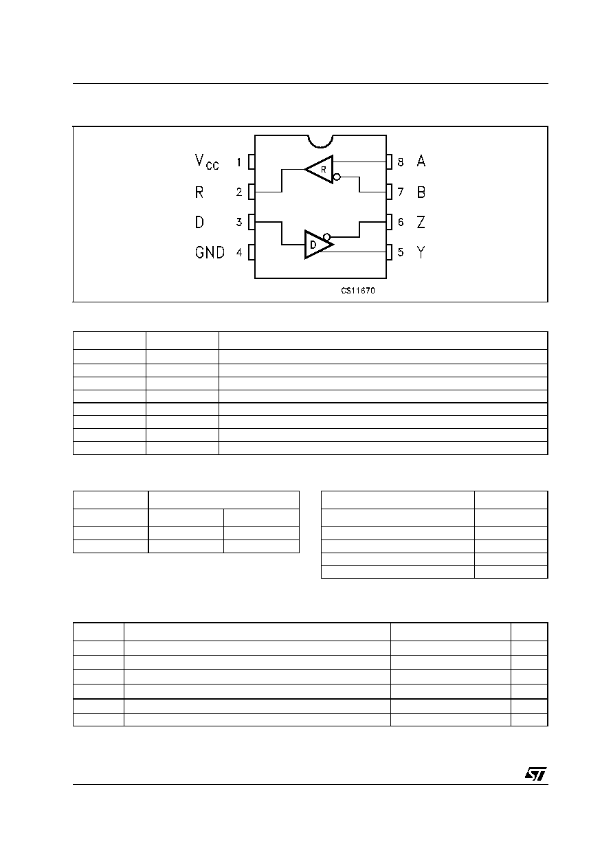
PIN CONFIGURATION
PIN DESCRIPTION
TRUTH TABLE (DRIVER)
X= Don't Care; Z=High Impedance
TRUTH TABLE (RECEIVER)
?= Irrelevant; Z=High Impedance
ABSOLUTE MAXIMUM RATINGS
Absolute Maximum Ratings are those values beyond which damage to the device may occur. Functional operation under these condition is
not implied.
PlN N∞
SYMBOL
NAME AND FUNCTION
1
V
CC
Supply Voltage
2
RO
Receiver Output.
3
DI
Driver Input.
4
GND
Ground
5
Z
Inverting Driver Output
6
Y
Non-inverting Driver Output
7
B
Inverting Receiver Input
8
A
Non-inverting Receiver Input
INPUT
OUTPUTS
DI
Y
Z
L
L
H
H
H
L
DIFFERENTIAL INPUT
OUTPUT
A-B
RO
-0.2V
H
between -0.2V to 0.2V
?
-0.2V
L
OPEN
H
Symbol
Parameter
Value
Unit
V
CC
Supply Voltage
7
V
V
DI
Driver Input Voltage
-0.5 to 7
V
V
Y
, V
Z
Driver Output Voltage
-7.5 to 12.5
V
V
A
, V
B
Receiver Input Voltage
-7.5 to 12.5
V
V
RO
Receiver Output Voltage
-0.3 to (V
CC
+ 0.3)
V
ESD
Human Boby Model
3.5
KV
ST490A
3/11
ELECTRICAL CHARACTERISTICS
V
CC
= 4.5V to 5.5V, T
A
= -40 to 85∞C, unless otherwise specified. Typical values are referred to T
A
= 25∞C)
TRANSMITTER ELECTRICAL CHARACTERISTICS
V
CC
= 4.5V to 5.5V, T
A
= -40 to 85∞C, unless otherwise specified. Typical values are referred to T
a
= 25∞C)
Symbol
Parameter
Test Conditions
Min.
Typ.
Max.
Unit
I
SUPPLY
No Load Supply Current
2
5
mA
C
IN
Input Capacitance
1.8
pF
C
YZ
Driver Output Capacitance
1.2
pF
C
OUT
Output Capacitance
2.3
pF
Symbol
Parameter
Test Conditions
Min.
Typ.
Max.
Unit
V
OD1
Differential Drive Output
(No load)
V
CC
V
V
OD2
Differential Drive Output
(With Load)
R
L
= 54
(RS-422) (Figure 1)
1.5
2.6
5
V
V
OD3
Differential Drive Output
(With Load)
R
L
= 100
(RS-422) (Figure 1)
2
3
V
V
OD
Change in magnitude of
Driver Differential Output
Voltage for Complementary
Output States (Note1)
R
L
= 54
or 100
(Figure 1)
0
0.2
V
V
OC
Driver Common Mode
Output Voltage
R
L
= 54
(Figure 1)
1
3
V
V
OC
Change in magnitude of
Driver Common Mode
Output Voltage (Note1)
R
L
= 54
(Figure 1)
0
0.2
V
I
OFF
Power Off Output Current
V
CC
= 0V
V
O
=-7V to 12V
±
100
µ
A
I
OSD
Driver Short Circuit Output
Current
V
O
=-7V to 12V
±
35
±
250
mA
V
IL
Input Logic Threshold Low
0.8
V
V
IH
Input Logic Threshold High
2
V

ST490A
4/11
RECEIVER ELECTRICAL CHARACTERISTICS
V
CC
= 4.5V to 5.5V, T
A
= -40 to 85∞C, unless otherwise specified. Typical values are referred to T
a
= 25∞C)
DRIVER SWITCHING CHARACTERISTICS
V
CC
= 4.5V to 5.5V, T
A
= -40 to 85∞C, unless otherwise specified. Typical values are referred to T
a
= 25∞C)
RECEIVER SWITCHING CHARACTERISTICS
V
CC
= 4.5V to 5.5V, T
A
= -40 to 85∞C, unless otherwise specified. Typical values are referred to T
a
= 25∞C)
Symbol
Parameter
Test Conditions
Min.
Typ.
Max.
Unit
I
IN1
Logic Input Current
±
2.0
µ
A
I
IN2
Input Current (A, B)
other input=0V
V
CC
= 0 or 5.25V
V
IN
=12V
0.5
1
mA
V
IN
=-7V
-0.35
-0.8
mA
V
TH
Receiver Differential
Threshold Voltage
V
CM
= -7V to 12V
-0.2
0.2
V
V
TH
Receiver Input Hysteresis
V
CM
= 0V
70
mV
V
OH
Receiver Output High
Voltage
I
OUT
= -8mA, V
ID
= 200mV
3.5
4.7
V
V
OL
Receiver Output Low
Voltage
I
OUT
= 8mA, V
ID
= -200mV
0.2
0.4
V
R
RIN
Receiver Input Resistance
V
CM
= -7V to 12V
12
24
K
I
OSR
Receiver Short-Circuit
Current
V
O
= 0V to V
CC
7
95
mA
Symbol
Parameter
Test Conditions
Min.
Typ.
Max.
Unit
D
R
Maximum Data Rate
Jitter <5%
25
50
Mbps
t
PLH
t
PHL
Propagation Delay Input to
Output
R
L
= 54
C
L1
=C
L2
=50pF, (Figure 1)
10
16
ns
t
SKEW
Differential Output Delay
Skew
R
L
= 54
C
L1
=C
L2
=50pF, (Figure 1)
1
3
ns
t
TLH
t
THL
Rise or Fall Differential
Time
R
L
= 54
C
L1
=C
L2
=50pF, (Figure 1)
8
12
ns
Symbol
Parameter
Test Conditions
Min.
Typ.
Max.
Unit
t
PLH
t
PHL
Propagation Delay Input to
Output
C
L
= 15pF
(Figures 2,4)
19
30
ns
t
SKD
|t
PLH -
t
PHL
| Receiver Output
Skew
C
L
= 15pF
(Figures 2,4)
1
3
ns
t
TLH
t
THL
Rise or Fall Time
C
L
= 15pF
(Figures 2,4)
8
ns
ST490A
5/11
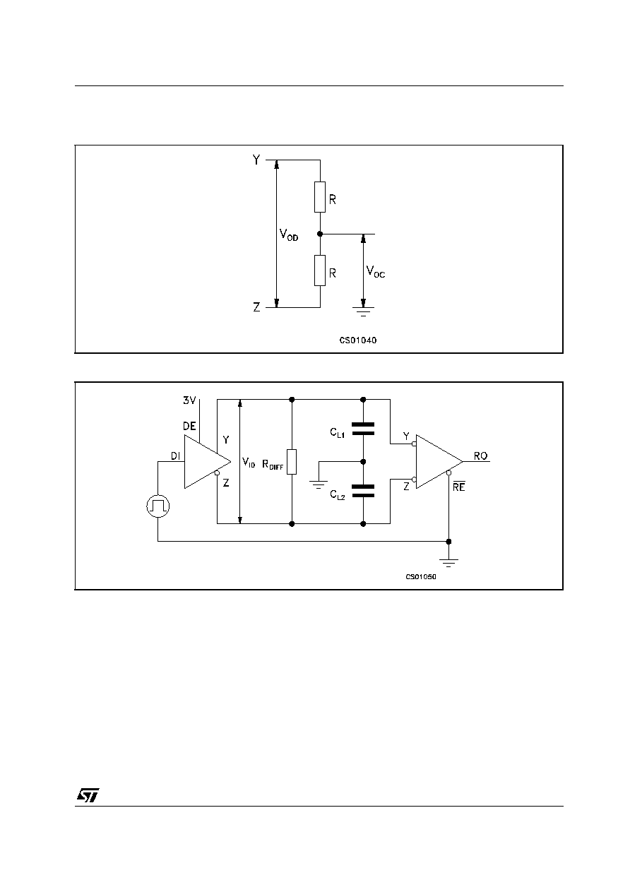
TEST CIRCUITS AND TYPICAL CHARACTERISTICS
Figure 1 : Driver DC Test Load
Figure 2 : Driver/Receiver Timing Test Circuit