ST5092
2.7V SUPPLY 14-BIT LINEAR CODEC
WITH HIGH-PERFORMANCE AUDIO FRONT-END
PRELIMINARY DATA
FEATURES:
Complete CODEC and FILTER system including:
14 BIT LINEAR ANALOG TO DIGITAL AND
DIGITAL TO ANALOG CONVERTERS.
8 BIT COMPANDED ANALOG TO DIGITAL
AND DIGITAL TO ANALOG CONVERTERS
A-LAW OR
µ
-LAW.
TRANSMIT AND RECEIVE BAND-PASS FILTERS
ACTIVE ANTIALIAS NOISE FILTER.
Phone Features:
THREE SWITCHABLE MICROPHONE AM-
PLIFIER INPUTS. GAIN PROGRAMMABLE:
20 dB PREAMP. (+MUTE), 0 . . 22.5 dB AM-
PLIFIER, 1.5 dB STEPS.
EARPIECE AUDIO OUTPUT. ATTENUATION
PROGRAMMABLE: 0 . . 30 dB, 2 dB STEPS.
EXTERNAL AUDIO OUTPUT. ATTENUATION
PROGRAMMABLE: 0 . . 30 dB, 2 dB STEPS.
TRANSIENT SUPRESSION SIGNAL DURING
POWER
ON
AND
DURING
AMPLIFIER
SWITCHING.
INTERNAL
PROGRAMMABLE
SIDETONE
CIRCUIT. ATTENUATION PROGRAMMABLE:
16 dB RANGE, 1 dB STEP. ROUTING POSSI-
BLE TO BOTH OUTPUTS.
INTERNAL RING OR TONE GENERATOR IN-
CLUDING DTMF TONES, SINEWAVE OR
SQUAREWAVE
WAVEFORMS.
ATTENU-
ATION PROGRAMMABLE: 27dB RANGE,
3dB STEP. THREE FREQUENCY RANGES:
a) 3.9Hz . . . . 996Hz, 3.9Hz STEP
b) 7.8Hz . . . . 1992Hz, 7.8Hz STEP
c) 15.6Hz . . . . 3984Hz, 15.6Hz STEP
PROGRAMMABLE PULSE WIDTH MODU-
LATED BUZZER DRIVER OUTPUT.
General Features:
SINGLE 2.7V to 3.6V SUPPLY
EXTENDED TEMPERATURE RANGE OPERA-
TION (*) -40
∞
C to 85
∞
C.
1.5
µ
W STANDBY POWER (TYP. AT 3.0V).
15mW OPERATING POWER (TYP. AT 3.0V).
13mW OPERATING POWER (TYP. AT 2.7V).
CMOS COMPATIBLE DIGITAL INTERFACES.
PROGRAMMABLE PCM AND CONTROL IN-
TERFACE MICROWIRE COMPATIBLE.
APPLICATIONS:
GSM DIGITAL CELLULAR TELEPHONES.
CT2 DIGITAL CORDLESS TELEPHONES.
DECT DIGITAL CORDLESS TELEPHONES.
BATTERY OPERATED AUDIO FRONT-ENDS
FOR DSPs.
(*) Functionality guaranteed in the range ≠ 40
∞
C to +85
∞
C;
Timing and Electrical Specifications are guaranteed in the range
≠ 30
∞
C to +85
∞
C.
GENERAL DESCRIPTION
ST5092 is a high performance low power combined
PCM CODEC/FILTER device tailored to implement
the audio front-end functions required by the next
generation low voltage/low power consumption
digital terminals.
ST5092 offers a number of programmable func-
tions accessed through a serial control channel that
easily interfaces to any classical microcontroller.
The PCM interface supports both non-delayed (nor-
mal and reverse) and delayed frame synchroniza-
tion modes.
ST5092 can be configurated either as a 14-bit lin-
ear or as an 8-bit companded PCM coder.
Additionally
to
the
CODEC/FILTER
function,
ST5092 includes a Tone/Ring/DTMF generator, a
sidetone generation, and a buzzer driver output.
ST5092 fulfills and exceeds D3/D4 and CCITT rec-
ommendations and ETSI requirements for digital
handset terminals.
Main applications include digital mobile phones, as
cellular and cordless phones, or any battery pow-
ered equipment that requires audio codecs operat-
ing at low single supply voltages
This is preliminary information on a new product now in development or undergoing evaluation. Details are subject to change without notice.
June 1997
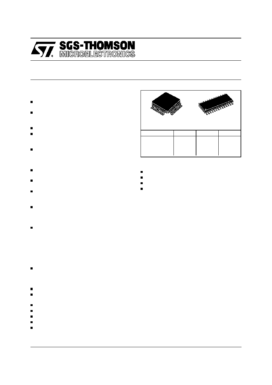
TQFP44(10x10x1.4)
SO28
ORDERING NUMBERS:
Package
Dim.
Cond.
ST5092AD
ST5092ADTR
ST5092TQFP
ST5092TQFPTR
SO28
SO28
TQFP44
TQFP44
10x10x1.4
10x10x1.4
Tube
Tape&Reel
Tray 8x20
Tape&Reel
1/29
VS & TE
MIC PREAMP
20dB
+ MUTE
MIC AMP
0 -> 22.5
1.5dB STEP
DE
(A)
(B)
PREFILTER &
BANDPASS
FILTER
PCM ADC
BANDPASS
FILTER
PCM DAC
TRANSMIT
REGISTER
RECEIVE
REGISTER
-1
1
12dB
-1
1
12dB
OE
TONE, RING
& DTMF
GENER.
& FILTER
EARA OUTPUT
0 -> -30dB,
2dB STEP
EXTA OUTPUT
RTE
SE
SI
TONE AMP
0 -> -27dB
3dB STEP
SIDETONE AMP
-12.5 -> -27.5dB
1dB STEP
CONTROL INTERFACE
µ
-WIRE
CLOCK GENERATOR
& SYNCHRONIZER
INTERFACE LATCH
BUZZER
DRIVER
BE
EN
EN
GNDP
GNDA
GND
VCCA
VCC
VCCP
LEVEL ADJUST
(PWM)
MIC3-
MIC2-
MIC1-
MIC2+
MIC1+
MIC3+
VFr+
VFr-
VLr-
VLr+
DX
CO
DR
CI
CS-
CCLK
FS
MCLK
LO
BZ
D93 TL074
BLOCK DIAGRAM
PIN CONNECTIONS (Top view)
N.C.
V
CCA
V
CCP
N.C.
V
Fr-
V
Lr-
V
Fr+
V
Lr+
GNDP
MCLK
LO
MIC2-
MIC1-
MIC2+
MIC1+
GNDA
MIC3-
MIC3+
1
3
2
4
5
6
7
8
9
26
25
24
23
22
20
21
19
27
10
28
D
R
FS
D94TL094
CCLK
CS-
CI
CO
D
x
GND
11
12
13
18
16
17
15
14
BZ
V
CC
1
2
3
5
6
4
7
8
9
10
17
11
18
19
20
21
22
44
43
42
41
39
40
38
37
36
35
34
28
27
26
24
23
25
33
32
31
29
30
VLr+
VLr-
N.C.
VFr-
N.C.
VFr+
N.C.
DR
N.C.
N.C.
GNDP
N.C.
N.C.
CCLK
CS-
BZ
CI
VCC
CO
DX
GND
N.C.
N.C.
N.C.
VCCP
VCCA
N.C.
N.C.
MIC3+
MIC3-
GNDA
N.C.
MIC1+
N.C.
N.C.
LO
FS
N.C.
MCLK
MIC1-
N.C.
MIC2+
N.C.
MIC2-
D94TL095
12
13
14
15
16
TQFP44
SO28
ST5092
2/29
PIN FUNCTIONS (SO28)
Pin
Name
Description
1
N.C.
Not Connected.
2
V
CCA
Positive power supply input for the analog section.
V
CC
and V
CCA
must be directly connect ed t oget her.
3
V
CCP
Positive power supply input for the power section. V
CCP
and V
CC
must be connected together.
4
N.C.
Not Connected.
5,6
V
Fr+
, V
Fr≠
Receive analog earpiece amplifier complementary outputs. These outputs can drive directly earpiece
transductor. The signal at this output can be the sum of:
- Receive Speech signal from D
R
,
- Internal Tone Generator,
- Sidetone signal.
7,8
V
Lr+
, V
Lr≠
Receive analog extra amplifier complementary outputs. The signal at these outputs can be the
sum of:
- Receive Speech signal from DR,
- Internal Tone generator,
- Sidetone signal.
9
GNDP
Power ground. V
Fr
and V
Lr
driver are referenced to this pin. GNDP and GND must be connected
together close to the device.
10
D
R
Receive data input: Data is shifted in during the assigned Received time slots In delayed and non-
delayed normal frame synchr. modes voice data byte is shifted in at the MCLK frequency on the
falling edges of MCLK, while in non-delayed reverse frame synchr. mode voice data byte is shifted in
at the MCLK frequency on the rising edges of MCLK.
11
CCLK
Control Clock input: This clock shifts serial control information into CI and out from CO when the
CS- input is low, depending on the current instruction. CCLK may be asynchronous with the other
system clocks.
12
CS-
Chip Select input: When this pin is low, control information is written into and out from the ST5092
via CI and CO pins.
13
CI
Control data Input: Serial Control information is shifted into the ST5092 on this pin when CS- is low
on the rising edges of CCLK.
14
BZ
Pulse width modulated buzzer driver output.
15
V
CC
Positive power supply input for the digital section.
16
CO
Control data Output: Serial control/status information is shifted out from the ST5092 on this pin
when CS- is low on the falling edges of CCLK.
17
D
X
Transmit Data ouput: Data is shifted out on this pin during the assigned transmit time slots.
Elsewhere D
X
output is in the high impedance state. In delayed and non-delayed normal frame
synchr. modes, voice data byte is shifted out from TRISTATE output D
X
at the MCLK on the rising
edge of MCLK, while in non-delayed reverse frame synchr mode voice data byte is shifted out on
the falling edge of MCLK.
18
GND
Ground: All digital signals are referenced to this pin.
19
FS
Frame Sync input: This signal is a 8kHz clock which defines the start of the transmit and receive
frames. Any of three formats may be used for this signal: non delayed normal mode, delayed
mode, and non delayed reverse mode.
20
MCLK
Master Clock Input: This signal is used by the switched capacitor filters and the encoder/decoder
sequencing logic. Values must be 512 kHz, 1.536 MHz, 2.048 MHz or 2.56 MHz selected by means of
Control Register CRO. MCLK is used also to shift-in and out data.
21
LO
A logic 1 written into DO (CR1) appears at LO pin as a logic 0
A logic 0 written into DO (CR1) appears at LO pin as a logic 1.
22
MIC2-
Second negative high impedance input to transmit pre-amplifier for microphone connection.
23
MIC2+
Second Positive high impedance input to transmit pre-amplifier for microphone connection.
24
MIC1-
Negative high impedance input to transmit pre-amplifier for microphone connection.
25
MIC1+
Positive high impedance input to transmit pre-amplifier for microphone connection.
26
GNDA
Analog Ground: All analog signals are referenced to this pin. GND and GNDA must be connected
together close to the device.
27
MIC3-
Third negative high impedance output to transmit preamplifier for microphone connection.
28
MIC3+
Third positive high impedance output to transmit preamplifier for microphone connection.
ST5092
3/29

PIN FUNCTIONS (TQFP44)
Pin
Name
Description
1
N.C.
Not Connected.
2,3
V
Fr+
, V
Fr≠
Receive analog earpiece amplifier complementary outputs. These outputs can drive directly earpiece
transductor. The signal at this output can be the summ of:
- Receive Speech signal from D
R
,
- Internal Tone Generator,
- Sidetone signal.
4
N.C.
Not Connected.
5,6
V
Lr+
, V
Lr≠
Receive analog extra amplifier complementary outputs. The signal at these outputs can be the sum of:
- Receive Speech signal from DR,
- Internal Tone generator,
- Sidetone signal.
7
N.C.
Not Connected.
8
GNDP
Power ground. V
Fr
and V
Lr
driver are referenced to this pin. GNDP and GND must be connected
together close to the device.
9
N.C.
Not Connected.
10
D
R
Receive data input: Data is shifted in during the assigned Received time slots In delayed and non-
delayed normal frame synchr. modes voice data byte is shifted in at the MCLK frequency on the
falling edges of MCLK, while in non-delayed reverse frame sinchr. mode voice data byte is shifted
in at the MCLK frequency on the rising edges of MCLK.
11,12,13
N.C.
Not Connected.
14
CCLK
Control Clock input: This clock shifts serial control information into CI and out from CO when the
CS- input is low, depending on the current instruction. CCLK may be asynchronous with the other
system clocks.
15
CS-
Chip Select input: When this pin is low, control information is written into and out from the ST5092
via CI and CO pins.
16
CI
Control data Input: Serial Control information is shifted into the ST5092 on this pin when CS- is low
on the rising edges of CCLK.
17
BZ
Pulse width modulated buzzer driver output.
18
V
CC
Positive power supply input for the digital section.
19
CO
Control data Output: Serial control/status information is shifted out from the ST5092 on this pin
when CS- is low on the falling edges of CCLK.
20
D
X
Transmit Data ouput: Data is shifted out on this pin during the assigned transmit time slots. Elsewhere
D
X
output is in the high impendance state. In delayed and non-delayed normal frame synchr. modes,
voice data byte is shifted out from TRISTATE output D
X
at the MCLK on the rising edge of MCLK, while
in non-delayed reverse frame synchr mode voice data byte is shifted out on the falling edge of MCLK.
21
GND
Ground: All digital signals are referenced to this pin.
22,23
N.C.
Not Connected.
24
FS
Frame Sync input: This signal is a 8kHz clock which defines the start of the transmit and receive
frames. Either of three formats may be used for this signal: non delayed normal mode, delayed
mode, and non delayed reverse mode.
25
MCLK
Master Clock Input: This signal is used by the switched capacitor filters and the encoder/decoder
sequencing logic. Values must be 512 kHz, 1.536 MHz, 2.048 MHz or 2.56 MHz selected by means of
Control Register CRO. MCLK is used also to shift-in and out data.
26
LO
A logic 1 written into DO (CR1) appears at LO pin as a logic 0
A logic 0 written into DO (CR1) appears at LO pin as a logic 1.
27,28,29
N.C.
Not Connected.
30
MIC2-
Second negative high impedance input to transmit pre-amplifier for microphone connection.
31
MIC2+
Second Positive high impedance input to transmit pre-amplifier for microphone connection.
32
N.C.
Not Connected.
33
MIC1-
Negative high impedance input to transmit pre-amplifier for microphone connection.
34
MIC1+
Positive high impedance input to transmit pre-amplifier for microphone connection.
35
N.C.
Not Connected.
36
GNDA
Analog Ground: All analog signals are referenced to this pin. GND and GNDA must be connected
together close to the device.
37
MIC3-
Third negative high impedance output to transmit preamplifier for microphone connection.
38
MIC3+
Third positive high impedance output to transmit preamplifier for microphone connection.
39,40
N.C.
Not Connected.
41
V
CCA
Positive power supply input for the analog section.
V
CC
and V
CCA
must be directly connect ed t oget her.
42
V
CCP
Positive power supply input for the power section. V
CCP
and V
CC
must be connected together.
43,44
N.C.
Not Connected.
ST5092
4/29

FUNCTIONAL DESCRIPTION
I
DEVICE OPERATION
I
.1 Power on initialization:
When power is first applied, power on reset cir-
cuitry initializes ST5092 and puts it into the power
down state. Gain Control Registers for the various
programmable gain amplifiers and programmable
switches are initialized as indicated in the Control
Register description section. All CODEC functions
are disabled.
The desired selection for all programmable func-
tions may be intialized prior to a power up com-
mand using the MICROWIRE control channel.
I
.2 Power up/down control:
Following power-on initialization, power up and
power down control may be accomplished by writ-
ing any of the control instructions listed in Table 1
into ST5092 with "P" bit set to 0 for power up or 1
for power down.
Normally, it is recommended that all programma-
ble functions be initially programmed while the
device is powered down. Power state control can
then be included with the last programming in-
struction or in a separate single byte instruction.
Any of the programmable registers may also be
modified while ST5092 is powered up or down by
setting "P" bit as indicated. When power up or
down control is entered as a single byte instruc-
tion, bit 1 must be set to a 0.
When a power up command is given, all de-acti-
vated circuits are activated, but output D
X
will re-
main in the high impedance state until the second
Fs pulse after power up.
I
.3 Power down state:
Following a period of activity, power down state
may be reentered by writing a power down in-
struction.
Control Registers remain in their current state and
can be changed by MICROWIRE control inter-
face.
In addition to the power down instruction, detec-
tion of loss MCLK (no transition detected) auto-
matically enters the device in "reset" power down
state with D
X
output in the high impedance state.
I
.4 Transmit section:
Transmit analog interface is designed in two
stages to enable gains up to 42.5 dB to be real-
ized. Stage 1 is a low noise differential amplifier
providing 20 dB gain. A microphone may be ca-
pacitevely connected to MIC1+, MIC1- inputs,
while the MIC2+ MIC2≠ and MIC3+ MIC3- inputs
may be used to capacitively connect a second mi-
crophone or a third microphone respectively or an
auxiliary audio circuit. MIC1 or MIC2 or MC3 or
transmit mute is selected with bits 6 and 7 of reg-
ister CR4.
In the mute case, the analog transmit signal is
grounded and the sidetone path is also disabled.
Following the first stage is a programmable gain
amplifier which provides from 0 to 22.5 dB of ad-
ditional gain in 1.5dB step. The total transmit gain
should be adjusted so that, at reference point A,
see Block Diagram description, the internal 0
dBm0 voltage is 0.49 Vrms (overload level is 0.7
Vrms). Second stage amplifier gain can be pro-
grammed with bits 4 to 7 of CR5.
An active RC prefilter then precedes the 8th order
band pass switched capacitor filter. A/D converter
can be either a 14-bit linear (bit CM = 0 in register
CR0) or can have a compressing characteristics
(bit CM = 1 in register CR0) according to CCITT A
or MU255 coding laws. A precision on chip volt-
age reference ensures accurate and highly stable
transmission levels.
Any offset voltage arising in the gain-set amplifier,
the filters or the comparator is cancelled by an in-
ternal autozero circuit.
Each encode cycle begins immediatly at the be-
ginning of the selected Transmit time slot. The to-
tal signal delay referenced to the start of the time
slot is approximatively 195
µ
s (due to the transmit
filter) plus 125
µ
s (due to encoding delay), which
totals 320
µ
s. Voice data is shifted out on D
X
dur-
ing the selected time slot on the transmit rising
edges of MCLK in delayed or non-delayed normal
mode or on the falling edges of MCLK in non-de-
layed reverse mode.
I
.5 Receive section:
Voice Data is shifted into the decoder's Receive
voice data Register via the D
R
pin during the se-
lected time slot on the falling edges of MCLK in
delayed or non-delayed normal mode or on the
rising edges of MCLK in non-delayed reverse
mode.
The decoder consists of either a 14-bit linear or
an expanding DAC with A or MU255 law decod-
ing characteristic. Following the Decoder is a
3400 Hz 8th order band-pass switched capacitor
filter with integral Sin X/X correction for the 8 kHz
sample and hold.
0 dBmO voltage at this (B) reference point (see
Block Diagram description) is 0.49 Vrms. A tran-
scient suppressing circuitry ensure interference
noise suppression at power up.
The analog speech signal output can be routed
either to earpiece (V
FR+
, V
FR-
outputs) or to an ex-
tra analog output (V
Lr+
, V
Lr-
outputs) by setting
bits OE and SE (1 and 0 of CR4).
Total signal delay is approximatively 190
µ
s (filter
plus decoding delay) plus 62.5
µ
s (1/2 frame)
which gives approximatively 252
µ
s.
Differential outputs V
FR+
,V
FR-
are intended to di-
rectly drive an earpiece. Preceding the outputs is
a programmable attenuation amplifier, which must
ST5092
5/29