 | –≠–ª–µ–∫—Ç—Ä–æ–Ω–Ω—ã–π –∫–æ–º–ø–æ–Ω–µ–Ω—Ç: ST52T301P | –°–∫–∞—á–∞—Ç—å:  PDF PDF  ZIP ZIP |
Æ
ST52T301/E301
8-Bit OTP/EPROM
DuaLogic
TM
MCUs WITH ADC,
UART, TIMER, TRIAC & PWM DRIVER
ADVANCED DATA SHEET
High Speed dedicated structures for Fuzzy Logic
(3.5
µ
s to compute a 4 In x 1 Out rule)
Capability to perform simple boolean and
arithmetic operations
Up to 4 Input, 2 Output ConfigurableVariables for
each Fuzzy Algorithm and up to 300 Rules
Up to 16 Triangular and Trapezoidal Membership
Functions for each Input variable
Up to 256 Singleton Membership Functions for
all Consequents
Program and Data EPROM: 2 Kbytes
16 general purpose registers ava ilable as
Register File
Working Clock Frequencies: 5, 10 and 20MHz
On-Chip Clock Oscillator driven by Quartz
Crystal or Ceramic Resonator
One external interrupt
Standard TTL compatible input
CMOS compatible output
4 channel 8 bit Analog to Digital Converter
Bandgap reference 2.5V
Digital 8 bit I/O port indepedently programmable
with handshake signal
S e r i al
C om m u n ic at i o n In t er fa ce wi t h
asynchronous protocol (UART)
Programmable Timer with internal Prescaler
Internal Power Fuzzy Control to drive external
Triac (up to 25mA source, 50 mA sink current)
Internal Fuzzy controlled PWM to drive an
external power device
Software tools and Emulators availability
Windowed and One Time Programmable (OTP)
Memory parts available for prototyping and
production phases
44 pin Plastic (PLCC44) and Ceramic Windowed
Leaded Chip Carrier (CLCC44-W)
July 1998
CLCC44-W
PLCC44
1.1 GENERAL DESCRIPTION
ST52E301
(1)
and ST52T301
(1)
devices are
members of the W.A.R.P.family of 8-bit
DuaLogic
TM
microcontrollers. They are able to perform, in an
efficient way, both booleanand fuzzy algorithms, in
order to reach the best performances that the two
methodologies allow.
The ST52E301is the erasableEPROMversion and
the ST52T301 is the OTP version.
The ST52x301 is completely developed and
produced by STMicroelectronics using the reliable
high performance CMOSM5E (O.7
µ
m) process.
Thanks to Fuzzy Logic, ST52x301 allows to
describe a problem using a linguistic model instead
of a mathematicalmodel. In thisway it is very useful
and easy to modelize complex system with very
high accuracy.
The linguistic approach is based on a set of
IF-THEN rules, describing the control behaviour,
and on Membership Functions associated to input
and output variables.
Fuzzy Inference is a set of operations which
computes the output values according with the
truth values of the involved rules.
Note: (1) Formerly W.A.R.P.3TC
1/99
The flexible I/O configuration of ST52x301 allows
to interface with a wide range of external devices,
like D/A converters, power control devices (SCRs,
TRIACs) and external sensors.
The OTP (One Time Programmable) device is fully
compatible with the EPROM windowed version,
which may be used to create prototype systems
and for the pre-production phases.
The Fuzzy Core includes the fuzzifier (ALPHA
calculator), the inference unit and the defuzzifier.
It allows to manage up to 300 Rules (4 Inputs and
1 Output). The rules could be shared in different
fuzzy subroutines that can be activated by user
defined conditions.
T he
I / O
c a p ab i l it i e s,
de m an d ed
f r om
microcontroller applications, are fulfilled by
ST52x301 with 4 Analog Inputs, an asynchronous
Peripheral interface (UART) and an 8-bit I/O
communicationport in orderto transferdata from/to
the on-chip Register File.
The voltage reference provides biasing to the
analog portion of the internal circuitry. The internal
reference is a 2.5V Bandgap reference.
The voltage reference can supply up to 0.1 mA of
current to power external circuitry.
ST52x301 includes an 8-bit sampling Analog to
Dig it al (A/ D) C o n ve r te r w i t h a 4 a n a lo g
channel fa st multiplexer (32
µ
s c o n ve rs i o n
time/channel).
It is possible to perform operations on data stored
in the Register File (16 bytes), allowing to manage
new inputs and feedback outputs.
The TRIAC/PWM Driver peripheral allows to
manage directly power devices, implementing
three different operating modes: Burst Mode
( i. e.T h e r m al A pp li ca t ion s) , Ph a s e A ng le
Partialization (i.e. Motors Control by TRIACs) and
high frequency PWM controls.
A programmable Timer with Internal Prescaler,
using both internal or external clock, is available.
The microcontroller configuration is stored in the
internal EPROM.
A
p o we r f u l
de vel o pm en t
e nvi r on m e nt ,
FUZZYSTUDIO
TM
3.0, consisting of a board
a n d s o f t w a r e t o o l s , a l l o w s a n e a s y
configuration and use of ST52x301.
S T 5 2 x 3 0 1
i s
f u l l y
s u p p o r t e d
b y
FUZZYSTUDIO3.0 so f t wa r e t o ols a llow in g
to gra ph ic al ly d es ig n a project and obtain an
optimized microcode.
ST52x301 exploits a SGS-THOMSON patented
strategy to store the MFs in its internal memory.
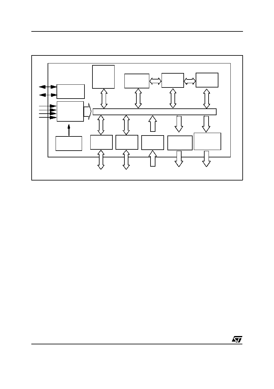
OSCILLATO R
ALU
-
FUZZY
CORE
SYSTEM
REGISTERS
CONTROL
UNIT
REGISTER
FILE
PARALLEL
I/O PORT
2kBytes
EPROM
TRIAC/PWM
DRIVE R
PROG.TIMER
WITH
PRESC ALER
SCI
A/D
CONVERT ER
BAND-GAP
REFERENCE
Figure 1. ST52x301 Architectural Block Diagram
2/99
ST52T301/E301
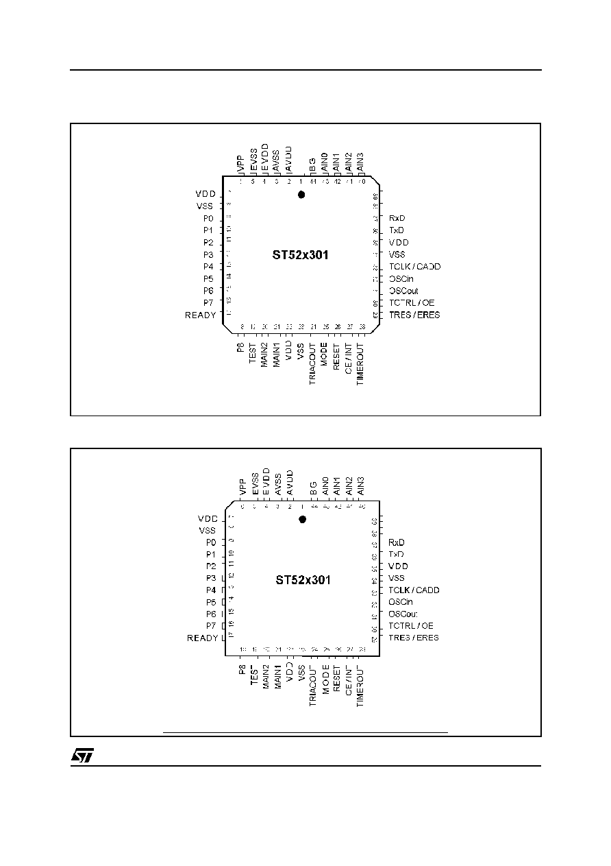
Figure 2. CLCC44-W Pin Configuration
Figure 3. PLCC44 Pin Configuration
3/99
ST52T301/E301

PIN
NAME
TYPE
Programming Phase
Working Phase
1
not connected
-
-
2
AV
DD
Analog V
DD
Analog V
DD
3
AV
SS
Analog Ground
Analog Ground
4
EV
DD
EPROM Digital Power Supply
EPROM Digital Power Supply
5
EV
SS
EPROM Digital Ground
EPROM Digital Ground
6
V
PP
EPROM Programming
Power supply (12V
±5%)
EPROM V
DD
(5V
±10%)
7
V
DD
Digital Power Supply
Digital Power Supply
8
V
SS
Digital Ground
Digital Ground
9
P0
I/O
I/O EPROM Data
Digital I/O
10
P1
I/O
I/O EPROM Data
Digital I/O
11
P2
I/O
I/O EPROM Data
Digital I/O
12
P3
I/O
I/O EPROM Data
Digital I/O
13
P4
I/O
I/O EPROM Data
Digital I/O
14
P5
I/O
I/O EPROM Data
Digital I/O
15
P6
I/O
I/O EPROM Data
Digital I/O
16
P7
I/O
I/O EPROM Data
Digital I/O
17
READY
O
I/O port Handshaking Signal
18
P8
O
Digital Output
19
TEST
I
(must be set to 0)
(must be set to 0)
20
MAIN2
I/O
Zero Crossing/Prescaler Output
21
MAIN1
I
Zero Crossing
22
V
DD
Digital Power Supply
Digital Power Supply
23
V
SS
Digital Ground
Digital Ground
24
TRIACOUT
O
Triac/PWM Driver Output Pulses
25
MODE
I
Functionment Mode Selector
Functionment Mode Selector
26
RESET
I
General Reset
General Reset
27
CE/INT
I
Chip Enable EPROM
External Interrupt
28
TIMEROUT
O
Output Timer
29
ERES / TRES
I
EPROM Address Counter Reset
External Timer Reset
30
OE / TCTRL
I
EPROM Output Enable
Timer Start/Stop Signal
31
OSCout
I/O
Oscillator Output
Oscillator Output
32
OSCin
I
Oscillator Input
Oscillator Input
33
CADD / TCLK
I
EPROM Change Address Clock
Timer External Clock
34
V
SS
Digital Ground
Digital Ground
35
V
DD
Digital Power Supply
Digital Power Supply
36
TxD
O
SCI Output
37
RxD
I
SCI Input
38
not connected
-
-
39
not connected
-
-
40
AIN3
Ainp
Analog Input
41
AIN2
Ainp
Analog Input
42
AIN1
Ainp
Analog Input
43
AIN0
Ainp
Analog Input
44
BG
Aout
Band Gap Output
Table 1. PLCC44 and CLCC44-W Pin Configuration
4/99
ST52T301/E301

1.2 PIN DESCRIPTION
V
DD,
EV
DD,
V
SS
, EV
SS,
AV
DD
, AV
SS,
V
PP
. In order to
avoid noise disturbances, the power supply of the
digital part is kept separated from the power supply
of the analog part.
V
DD.
Main Power Supply Voltage (5V 10%).
V
SS
. Digital circuit Ground.
EV
DD.
EPROM Main Power Supply Voltage (5V
10%).
EV
SS
. EPROM Digital circuit Ground.
AV
DD
. Analog V
DD
of the Analog to Digital
Converter.
AV
SS
.AnalogV
SS
of theAnalog to DigitalConverter.
Must be tied to V
SS
.
V
PP
. Main Power Supply for the internal EPROM
(12.5V 5%).
OSCin and OSCout. These pins are internally
connected with the on-chip oscillator circuit. A
quar tz crystal or a ceramic resonator can be
connectedbetween these two pins in order to allow
the correct operations of ST52x301 with various
stability/cost trade-offs. An external clock signal
can be applied to OSCin, in this case OSCout must
be grounded.
RESET. This signal is used to restart ST52x301 at
the beginningof its program.It also allows to select
the program mode for the EPROM.
INT. External interrupt active on rising or falling
edge.
AIN0-AIN3. These 4 lines are connected to the
inputs of the analog multiplexer. They allow to
acquire 4 analog inputs.
BG. A Voltage equal to 2.5V is available on this pin.
It can be used for Analog signal conditioning.
P0-P7. These 8 lines are organizedas one I/O port.
During the Programming phase such port is used
for the EPROM data read/write.
READY. Handshake signal of the parallel port.
P8. Digital output.
TxD. Serial data output of
the SCI transmitter
block.
RxD. Serial data input of
the SCI receiver
block.
TRES, TCLK, TCTRL, TIMEROUT. These pins are
related with the internal Programmable Timer. The
Timer can be reset externally by using TRES. In
Working Mode, TRES resets the address counter
of the Timer. TRES is active at low level
The Timer Clock can be the internal clock or can
be supplied externally by using the pin TCLK.
An external Start/Stopsignal can be used to control
the Timer throughthe pin TCTRL.The Timeroutput
is available on the pin TIMEROUT.
MAIN1, MAIN2, TRIACOUT. ST52x301 is able to
drive a TRIAC in two different modes: Burst mode
or Phase Angle Partialization control mode.
The Burst mode is used for thermal regulation.
MAIN1 and MAIN2 signals are used to detect the
zero crossing of the main voltage.
The pulse to drivethe TRIACis givenby TRIACOUT
pin.
It is possible to use the same pins to implement a
PWM Driver. In this case it is possible to fix the
period of PWM and to change the duty cycle on fly.
The PWM output is given by TRIACOUT pin.
CE, OE, ERES, CADD, V
PP
. These pins are used
to manage the EPROM during the Programming
p ha s e . D ur i n g t h e P r o g ra m m i ng ph a se
(programming) V
PP
must be set at 12V. In the
Working phase V
PP
must be equal to V
DD
.
ERES in Programming Mode resets the address
counter of the EPROM; it is active at high level.
In the Working phase OE, CE and CADD are used
like handshaking signals for the parallel port.
MODE. I t s el ec ts t h e fun ct i on ment mo d e
(Programming or Working mode).
TEST. It enables the testing functionalities; during
the Programming and Working phaseit must be set
to 0.
5/99
ST52T301/E301