 | –≠–ª–µ–∫—Ç—Ä–æ–Ω–Ω—ã–π –∫–æ–º–ø–æ–Ω–µ–Ω—Ç: ST6210LB1 | –°–∫–∞—á–∞—Ç—å:  PDF PDF  ZIP ZIP |
November 1997
1/10
R
Rev. 1.0
ST6208L/09L
ST6210L/20L
LOW VOLTAGE 8-BIT ROM MCUs WITH
A/D CONVERTER AND 20 PINS
s
2.4 to 3.9V Supply Operating Range
s
4 MHz Maximum Clock Frequency
s
0 to +70
∞
C Operating Temperature Range
s
Run, Wait and Stop Modes
s
5 Interrupt Vectors
s
Look-up Table capability in Program Memory
s
Data Storage in Program Memory:
User selectable size
s
Data RAM: 64bytes
s
12 I/O pins, fully programmable as:
≠ Input with pull-up resistor
≠ Input without pull-up resistor
≠ Input with interrupt generation
≠ Open-drain or push-pull output
≠ Analog Input (except ST6208L)
s
4 I/O lines can sink up to 12mA to drive LEDs
s
8-bit Timer/ Counter with 7-bit programmable
prescaler
s
Digital Watchdog
s
8-bit A/D Converter with 8 analog inputs
s
On-chip Clock oscillator can be driven by Quartz
Crystal Ceramic resonator or RC network
s
Power-on Reset
s
One external Non-Maskable Interrupt
s
ST626x-EMU2 Emulation and Development
System (connects to an MS-DOS PC via an
RS232 serial line)
DEVICE SUMMARY
(See end of Datasheet for Ordering Information)
PDIP20
PSO20
DEVICE
ROM
(Bytes)
I/O Pins
Analog
inputs
ST62T08L
1036
12
-
ST62T09L
1036
12
4
ST62T10L
1836
12
8
ST62T20L
3884
12
8
1
2/10
ST6208L/09L ST6210L/20L
1 GENERAL DESCRIPTION
1.1 INTRODUCTION
The ST6208L/09L/10L/20L are low voltage mask
programmed ROM version of ST62T08C/T09C/
T10C/T20C OTP devices.
They offer the same functionality as OTP devices,
selecting as ROM options the options defined in
the programmable option byte of the OTP version,
with the exception of the LVD Reset that is not
available.
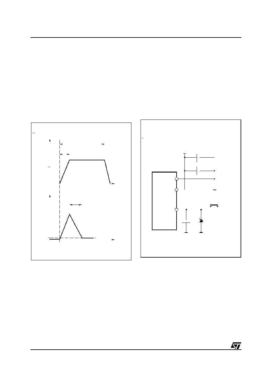
Figure 1. Programming wave form
1.2 ROM READOUT PROTECTION
If the ROM READOUT PROTECTION option is
selected, a protection fuse can be blown to pre-
vent any access to the program memory content.
In case the user wants to blow this fuse, high volt-
age must be applied on the TEST pin.
Figure 2. Programming Circuit
Note: ZPD15 is used for overvoltage protection
VR02001
0 .5s m in
15
1 0
5
1 4V typ
100 s max
t
t
4mA typ
100mA
150 s typ
max
TES T
TES T
VR02003
P ROTE CT
ZP D15
5V
V
S S
V
DD
TE S T
47
F
m
100nF
100nF
15V
14V
1

3/10
ST6208L/09L ST6210L/20L
ST6208L/09L/10L/20L MICROCONTROLLER OPTION LIST
Customer
. . . . . . . . . . . . . . . . . . . . . . . . . . . . .
Address
. . . . . . . . . . . . . . . . . . . . . . . . . . . . .
. . . . . . . . . . . . . . . . . . . . . . . . . . . . .
Contact
. . . . . . . . . . . . . . . . . . . . . . . . . . . . .
Phone No
. . . . . . . . . . . . . . . . . . . . . . . . . . . . .
Reference
. . . . . . . . . . . . . . . . . . . . . . . . . . . . .
SGS-THOMSON Microelectronics references
DeviLe:
[ ] ST6208L
[ ] ST6209L
[ ] ST6210L
[ ] ST6220L
Package:
[ ] Dual in Line Plastic [ ] Small Outline Plastic with conditionning:
[ ] Standard (Stick)
[ ] Tape & Reel
Temperature Range:
[ ] 0
∞
C to + 70
∞
C
Special Marking:
[ ] No
[ ] Yes "_ _ _ _ _ _ _ _ _ _ _ "
Authorized characters are letters, digits, '.', '-', '/' and spaces only.
Maximum character count: DIP20:
10
SO20:
8
Oscillator Source Selection: [ ] Crystal Quartz/Ceramic resonator
[ ] RC Network
Watchdog Selection:
[ ] Software Activation
[ ] Hardware Activation
ROM Readout Protection:
[ ] Disabled (Fuse cannot be blown)
[ ] Enabled (Fuse can be blown by the customer)
Note:
No part is delivered with protected ROM.
The fuse must be blown for protection to be effective.
External STOP Mode Control[ ] Enabled
[ ] Disabled
TIMER pin pull-up
[ ] Enabled
[ ] Disabled
NMI pin pull-up
[ ] Enabled
[ ] Disabled
Comments :
Supply Operating Range in the application:
Oscillator Fequency in the application:
Notes
. . . . . . . . . . . . . . . . . . . . . . . . . . . . .
Signature
. . . . . . . . . . . . . . . . . . . . . . . . . . . . .
Date
. . . . . . . . . . . . . . . . . . . . . . . . . . . . .
1
4/10
ST6208L/09L ST6210L/20L
1.3 ORDERING INFORMATION
The following section deals with the procedure for
transfer of customer codes to SGS-THOMSON.
1.3.1 Transfer of Customer Code
Customer code is made up of the ROM contents
and the list of the selected mask options. The
ROM contents are to be sent on diskette, or by
electronic means, with the hexadecimal file gener-
ated by the development tool. All unused bytes
must be set to FFh.
The selected mask options are communicated to
SGS-THOMSON using the correctly filled OP-
TION LIST appended.
1.3.2 Listing Generation and Verification
When SGS-THOMSON receives the user's ROM
contents, a computer listing is generated from it.
This listing refers exactly to the mask which will be
used to produce the specified MCU. The listing is
then returned to the customer who must thorough-
ly
check,
complete,
sign
and
return
it to
SGS-THOMSON. The signed listing forms a part
of the contractual agreement for the creation of the
specific customer mask.
The SGS-THOMSON Sales Organization will be
pleased to provide detailed information on con-
tractual points.
Table 1. ROM Memory Map for ST6208L,09L
Table 2. ROM Memory Map for ST6210L
Table 3. ROM Memory Map for ST6220L
Table 4. ROM version Ordering Information
Device Address
Description
0000h-0B9Fh
0BA0h-0F9Fh
0FA0h-0FEFh
0FF0h-0FF7h
0FF8h-0FFBh
0FFCh-0FFDh
0FFEh-0FFFh
Reserved
User ROM
Reserved
Interrupt Vectors
Reserved
NMI Interrupt Vector
Reset Vector
Device Address
Description
0000h-087Fh
0880h-0F9Fh
0FA0h-0FEFh
0FF0h-0FF7h
0FF8h-0FFBh
0FFCh-0FFDh
0FFEh-0FFFh
Reserved
User ROM
Reserved
Interrupt Vectors
Reserved
NMI Interrupt Vector
Reset Vector
Device Address
Description
0000h-007Fh
0080h-0F9Fh
0FA0h-0FEFh
0FF0h-0FF7h
0FF8h-0FFBh
0FFCh-0FFDh
0FFEh-0FFFh
Reserved
User ROM
Reserved
Interrupt Vectors
Reserved
NMI Interrupt Vector
Reset Vector
Sales Type
ROM
Analog input s
Temperature Range
Package
ST6208LB1/XXX
1036 Bytes
None
0 to +70
∞
C
PDIP20
ST6208LM1/XXX
PSO20
ST6209LB1/XXX
1036 Bytes
4
PDIP2
ST6209LM1/XXX
PSO20
ST6210LB1/XXX
1836 Bytes
8
PDIP20
ST6210LM1/XXX
PSO20
ST6220LB1/XXX
3884 Bytes
8
PDIP20
ST6220LM1/XXX
PSO20
1
5/10
ST6208L/09L ST6210L/20L
2 ELECTRICAL CHARACTERISTICS
2.1 ABSOLUTE MAXIMUM RATINGS
This product contains devices to protect the inputs
against damage due to high static voltages, how-
ever it is advisable to take normal precaution to
avoid application of any voltage higher than the
specified maximum rated voltages.
For proper operation it is recommended that V
I
and V
O
be higher than V
SS
and lower than V
DD
.
Reliability is enhanced if unused inputs are con-
nected to an appropriate logic voltage level (V
DD
or V
SS
).
Power Considerations.The average chip-junc-
tion temperature, Tj, in Celsius can be obtained
from:
Tj=TA + PD x RthJA
Where:TA = Ambient Temperature.
RthJA =Package thermal resistance (junc-
tion-to ambient).
PD = Pint + Pport.
Pint =IDD x VDD (chip internal power).
Pport =Port power dissipation (determined
by the user).
Notes:
-
Stresses above those listed as "absolute maximum ratings" may cause permanent damage to the device. This is a stress rating only and
functional operation of the device at these conditions is not implied. Exposure to maximum rating conditions for extended period s may
affect device reliability.
- (1) Wi thin these limits , clamping diodes are guarantee to be not conductive. Voltages outside these limits are authorised as long as injection
current is kept within the specification.
Symbol
Parameter
Value
Unit
V
DD
Supply Voltage
-0.3 to 7.0
V
V
I
Input Voltage
V
SS
- 0.3 to V
DD
+ 0.3
(1)
V
V
O
Output Voltage
V
SS
- 0.3 to V
DD
+ 0.3
(1)
V
I
O
Current Drain per Pin Excluding V
DD
, V
SS
±
10
mA
IV
DD
Total Current into V
DD
(source)
50
mA
IV
SS
Total Current out of V
SS
(sink)
50
mA
Tj
Junction Temperature
150
∞
C
T
STG
Storage Temperature
-60 to 150
∞
C
1