 | –≠–ª–µ–∫—Ç—Ä–æ–Ω–Ω—ã–π –∫–æ–º–ø–æ–Ω–µ–Ω—Ç: ST6252BB3 | –°–∫–∞—á–∞—Ç—å:  PDF PDF  ZIP ZIP |
April 1998
1/68
R
ST62T52B
ST62T62B/E62B
8-BIT OTP/EPROM MCUs WITH
A/D CONVERTER, AUTO-RELOAD TIMER AND EEPROM
s
3.0 to 6.0V Supply Operating Range
s
8 MHz Maximum Clock Frequency
s
-40 to +125∞C Operating Temperature Range
s
Run, Wait and Stop Modes
s
5 Interrupt Vectors
s
Look-up Table capability in Program Memory
s
Data Storage in Program Memory:
User selectable size
s
Data RAM: 128 bytes
s
Data EEPROM: 64 bytes (none on ST62T52B)
s
User Programmable Options
s
9 I/O pins, fully programmable as:
≠ Input with pull-up resistor
≠ Input without pull-up resistor
≠ Input with interrupt generation
≠ Open-drain or push-pull output
≠ Analog Input
s
5 I/O lines can sink up to 20mA to drive LEDs or
TRIACs directly
s
8-bit Timer/Counter with 7-bit programmable
prescaler
s
8-bit Auto-reload Timer with 7-bit programmable
prescaler (AR Timer)
s
Digital Watchdog
s
8-bit A/D Converter with 4 analog inputs
s
On-chip Clock oscillator can be driven by Quartz
Crystal Ceramic resonator or RC network
s
User configurable Power-on Reset
s
One external Non-Maskable Interrupt
s
ST626x-EMU2 Emulation and Development
System (connects to an MS-DOS PC via a
parallel port)
DEVICE SUMMARY
(See end of Datasheet for Ordering Information)
PDIP16
PSO16
CDIP16W
DEVICE
EPROM
(Bytes)
OTP
(Bytes)
EEPROM
ST62T52B
1836
-
ST62T62B
1836
64
ST62E62B
1836
64
1
Rev. 2.4

2/68
Table of Contents
68
2
ST62T52B / ST62T62B/E62B . . . . . . . . . . . . . . . . . . . . . . . . . . . 1
1 GENERAL DESCRIPTION . . . . . . . . . . . . . . . . . . . . . . . . . . . . . . . . . . . . . . . . . . . . . . . . . . . . . . 4
1.1 INTRODUCTION . . . . . . . . . . . . . . . . . . . . . . . . . . . . . . . . . . . . . . . . . . . . . . . . . . . . . . . . . 4
1.2 PIN DESCRIPTIONS . . . . . . . . . . . . . . . . . . . . . . . . . . . . . . . . . . . . . . . . . . . . . . . . . . . . . . 5
1.3 MEMORY MAP . . . . . . . . . . . . . . . . . . . . . . . . . . . . . . . . . . . . . . . . . . . . . . . . . . . . . . . . . . 6
1.3.1 Introduction . . . . . . . . . . . . . . . . . . . . . . . . . . . . . . . . . . . . . . . . . . . . . . . . . . . . . . . . 6
1.3.2 Program Space . . . . . . . . . . . . . . . . . . . . . . . . . . . . . . . . . . . . . . . . . . . . . . . . . . . . . 7
1.3.3 Data Space . . . . . . . . . . . . . . . . . . . . . . . . . . . . . . . . . . . . . . . . . . . . . . . . . . . . . . . . 8
1.3.4 Stack Space . . . . . . . . . . . . . . . . . . . . . . . . . . . . . . . . . . . . . . . . . . . . . . . . . . . . . . . . 8
1.3.5 Data Window Register (DWR) . . . . . . . . . . . . . . . . . . . . . . . . . . . . . . . . . . . . . . . . . . 9
1.3.6 Data RAM/EEPROM Bank Register (DRBR) . . . . . . . . . . . . . . . . . . . . . . . . . . . . . . 10
1.3.7 EEPROM Description . . . . . . . . . . . . . . . . . . . . . . . . . . . . . . . . . . . . . . . . . . . . . . . 11
1.4 PROGRAMMING MODES . . . . . . . . . . . . . . . . . . . . . . . . . . . . . . . . . . . . . . . . . . . . . . . . . 13
1.4.1 Option Byte . . . . . . . . . . . . . . . . . . . . . . . . . . . . . . . . . . . . . . . . . . . . . . . . . . . . . . . 13
1.4.2 Program Memory . . . . . . . . . . . . . . . . . . . . . . . . . . . . . . . . . . . . . . . . . . . . . . . . . . . 13
1.4.3 . EEPROM Data Memory . . . . . . . . . . . . . . . . . . . . . . . . . . . . . . . . . . . . . . . . . . . . . 13
2 CENTRAL PROCESSING UNIT . . . . . . . . . . . . . . . . . . . . . . . . . . . . . . . . . . . . . . . . . . . . . . . . . 14
2.1 INTRODUCTION . . . . . . . . . . . . . . . . . . . . . . . . . . . . . . . . . . . . . . . . . . . . . . . . . . . . . . . . 14
2.2 CPU REGISTERS . . . . . . . . . . . . . . . . . . . . . . . . . . . . . . . . . . . . . . . . . . . . . . . . . . . . . . . 14
3 CLOCKS, RESET, INTERRUPTS AND POWER SAVING MODES . . . . . . . . . . . . . . . . . . . . . 16
3.1 CLOCK SYSTEM . . . . . . . . . . . . . . . . . . . . . . . . . . . . . . . . . . . . . . . . . . . . . . . . . . . . . . . . 16
3.1.1 Main Oscillator . . . . . . . . . . . . . . . . . . . . . . . . . . . . . . . . . . . . . . . . . . . . . . . . . . . . . 16
3.2 RESETS . . . . . . . . . . . . . . . . . . . . . . . . . . . . . . . . . . . . . . . . . . . . . . . . . . . . . . . . . . . . . . . 18
3.2.1 RESET Input . . . . . . . . . . . . . . . . . . . . . . . . . . . . . . . . . . . . . . . . . . . . . . . . . . . . . . 18
3.2.2 Power-on Reset . . . . . . . . . . . . . . . . . . . . . . . . . . . . . . . . . . . . . . . . . . . . . . . . . . . . 18
3.2.3 Watchdog Reset . . . . . . . . . . . . . . . . . . . . . . . . . . . . . . . . . . . . . . . . . . . . . . . . . . . 19
3.2.4 Application Notes . . . . . . . . . . . . . . . . . . . . . . . . . . . . . . . . . . . . . . . . . . . . . . . . . . . 19
3.2.5 MCU Initialization Sequence . . . . . . . . . . . . . . . . . . . . . . . . . . . . . . . . . . . . . . . . . . 19
3.3 DIGITAL WATCHDOG . . . . . . . . . . . . . . . . . . . . . . . . . . . . . . . . . . . . . . . . . . . . . . . . . . . . 21
3.3.1 Digital Watchdog Register (DWDR) . . . . . . . . . . . . . . . . . . . . . . . . . . . . . . . . . . . . . 23
3.3.2 Application Notes . . . . . . . . . . . . . . . . . . . . . . . . . . . . . . . . . . . . . . . . . . . . . . . . . . . 23
3.4 INTERRUPTS . . . . . . . . . . . . . . . . . . . . . . . . . . . . . . . . . . . . . . . . . . . . . . . . . . . . . . . . . . 25
3.4.1 Interrupt request . . . . . . . . . . . . . . . . . . . . . . . . . . . . . . . . . . . . . . . . . . . . . . . . . . . . 25
3.4.2 Interrupt Procedure . . . . . . . . . . . . . . . . . . . . . . . . . . . . . . . . . . . . . . . . . . . . . . . . . 26
3.4.3 Interrupt Option Register (IOR) . . . . . . . . . . . . . . . . . . . . . . . . . . . . . . . . . . . . . . . . 27
3.4.4 Interrupt Sources . . . . . . . . . . . . . . . . . . . . . . . . . . . . . . . . . . . . . . . . . . . . . . . . . . . 27
3.5 POWER SAVING MODES . . . . . . . . . . . . . . . . . . . . . . . . . . . . . . . . . . . . . . . . . . . . . . . . . 29
3.5.1 WAIT Mode . . . . . . . . . . . . . . . . . . . . . . . . . . . . . . . . . . . . . . . . . . . . . . . . . . . . . . . 29
3.5.2 STOP Mode . . . . . . . . . . . . . . . . . . . . . . . . . . . . . . . . . . . . . . . . . . . . . . . . . . . . . . . 29
3.5.3 Exit from WAIT and STOP Modes . . . . . . . . . . . . . . . . . . . . . . . . . . . . . . . . . . . . . . 30
4 ON-CHIP PERIPHERALS . . . . . . . . . . . . . . . . . . . . . . . . . . . . . . . . . . . . . . . . . . . . . . . . . . . . . . 31
4.1 I/O PORTS . . . . . . . . . . . . . . . . . . . . . . . . . . . . . . . . . . . . . . . . . . . . . . . . . . . . . . . . . . . . . 31
4.1.1 Operating Modes . . . . . . . . . . . . . . . . . . . . . . . . . . . . . . . . . . . . . . . . . . . . . . . . . . . 32
4.1.2 Safe I/O State Switching Sequence . . . . . . . . . . . . . . . . . . . . . . . . . . . . . . . . . . . . . 33
4.1.3 ARTimer alternate functions . . . . . . . . . . . . . . . . . . . . . . . . . . . . . . . . . . . . . . . . . . 35
4.2 TIMER . . . . . . . . . . . . . . . . . . . . . . . . . . . . . . . . . . . . . . . . . . . . . . . . . . . . . . . . . . . . . . . . 36

3/68
Table of Contents
3
4.2.1 Timer Operation . . . . . . . . . . . . . . . . . . . . . . . . . . . . . . . . . . . . . . . . . . . . . . . . . . . . 37
4.2.2 Timer Interrupt . . . . . . . . . . . . . . . . . . . . . . . . . . . . . . . . . . . . . . . . . . . . . . . . . . . . . 37
4.2.3 Application Notes . . . . . . . . . . . . . . . . . . . . . . . . . . . . . . . . . . . . . . . . . . . . . . . . . . . 37
4.2.4 Timer Registers . . . . . . . . . . . . . . . . . . . . . . . . . . . . . . . . . . . . . . . . . . . . . . . . . . . . 38
4.3 AUTO-RELOAD TIMER . . . . . . . . . . . . . . . . . . . . . . . . . . . . . . . . . . . . . . . . . . . . . . . . . . . 39
4.3.1 AR Timer Description . . . . . . . . . . . . . . . . . . . . . . . . . . . . . . . . . . . . . . . . . . . . . . . . 39
4.3.2 Timer Operating Modes . . . . . . . . . . . . . . . . . . . . . . . . . . . . . . . . . . . . . . . . . . . . . . 39
4.3.3 AR Timer Registers . . . . . . . . . . . . . . . . . . . . . . . . . . . . . . . . . . . . . . . . . . . . . . . . . 43
4.4 A/D CONVERTER (ADC) . . . . . . . . . . . . . . . . . . . . . . . . . . . . . . . . . . . . . . . . . . . . . . . . . 45
4.4.1 Application Notes . . . . . . . . . . . . . . . . . . . . . . . . . . . . . . . . . . . . . . . . . . . . . . . . . . . 45
5 SOFTWARE . . . . . . . . . . . . . . . . . . . . . . . . . . . . . . . . . . . . . . . . . . . . . . . . . . . . . . . . . . . . . . . . 47
5.1 ST6 ARCHITECTURE . . . . . . . . . . . . . . . . . . . . . . . . . . . . . . . . . . . . . . . . . . . . . . . . . . . . 47
5.2 ADDRESSING MODES . . . . . . . . . . . . . . . . . . . . . . . . . . . . . . . . . . . . . . . . . . . . . . . . . . . 47
5.3 INSTRUCTION SET . . . . . . . . . . . . . . . . . . . . . . . . . . . . . . . . . . . . . . . . . . . . . . . . . . . . . . 48
6 ELECTRICAL CHARACTERISTICS . . . . . . . . . . . . . . . . . . . . . . . . . . . . . . . . . . . . . . . . . . . . . . 53
6.1 ABSOLUTE MAXIMUM RATINGS . . . . . . . . . . . . . . . . . . . . . . . . . . . . . . . . . . . . . . . . . . . 53
6.2 RECOMMENDED OPERATING CONDITIONS . . . . . . . . . . . . . . . . . . . . . . . . . . . . . . . . . 54
6.3 DC ELECTRICAL CHARACTERISTICS . . . . . . . . . . . . . . . . . . . . . . . . . . . . . . . . . . . . . . 55
6.4 AC ELECTRICAL CHARACTERISTICS . . . . . . . . . . . . . . . . . . . . . . . . . . . . . . . . . . . . . . 56
6.5 A/D CONVERTER CHARACTERISTICS . . . . . . . . . . . . . . . . . . . . . . . . . . . . . . . . . . . . . . 56
6.6 TIMER CHARACTERISTICS . . . . . . . . . . . . . . . . . . . . . . . . . . . . . . . . . . . . . . . . . . . . . . . 57
6.7 SPI CHARACTERISTICS . . . . . . . . . . . . . . . . . . . . . . . . . . . . . . . . . . . . . . . . . . . . . . . . . 57
6.8 ARTIMER ELECTRICAL CHARACTERISTICS . . . . . . . . . . . . . . . . . . . . . . . . . . . . . . . . . 57
7 GENERAL INFORMATION . . . . . . . . . . . . . . . . . . . . . . . . . . . . . . . . . . . . . . . . . . . . . . . . . . . . . 58
7.1 PACKAGE MECHANICAL DATA . . . . . . . . . . . . . . . . . . . . . . . . . . . . . . . . . . . . . . . . . . . . 58
7.2 ORDERING INFORMATION . . . . . . . . . . . . . . . . . . . . . . . . . . . . . . . . . . . . . . . . . . . . . . . 59
ST62P52B / ST62P62B . . . . . . . . . . . . . . . . . . . . . . . . . . . . . . . 61
1 GENERAL DESCRIPTION . . . . . . . . . . . . . . . . . . . . . . . . . . . . . . . . . . . . . . . . . . . . . . . . . . . . . 62
1.1 INTRODUCTION . . . . . . . . . . . . . . . . . . . . . . . . . . . . . . . . . . . . . . . . . . . . . . . . . . . . . . . . 62
1.2 ORDERING INFORMATION . . . . . . . . . . . . . . . . . . . . . . . . . . . . . . . . . . . . . . . . . . . . . . . 62
1.2.1 Transfer of Customer Code . . . . . . . . . . . . . . . . . . . . . . . . . . . . . . . . . . . . . . . . . . . 62
1.2.2 Listing Generation and Verification . . . . . . . . . . . . . . . . . . . . . . . . . . . . . . . . . . . . . 62
ST6252B / ST6262B . . . . . . . . . . . . . . . . . . . . . . . . . . . . . . . . . 65
1 GENERAL DESCRIPTION . . . . . . . . . . . . . . . . . . . . . . . . . . . . . . . . . . . . . . . . . . . . . . . . . . . . . 66
1.1 INTRODUCTION . . . . . . . . . . . . . . . . . . . . . . . . . . . . . . . . . . . . . . . . . . . . . . . . . . . . . . . . 66
1.2 ROM READOUT PROTECTION . . . . . . . . . . . . . . . . . . . . . . . . . . . . . . . . . . . . . . . . . . . . 66
1.3 ORDERING INFORMATION . . . . . . . . . . . . . . . . . . . . . . . . . . . . . . . . . . . . . . . . . . . . . . . 68
1.3.1 Transfer of Customer Code . . . . . . . . . . . . . . . . . . . . . . . . . . . . . . . . . . . . . . . . . . . 68
1.3.2 Listing Generation and Verification . . . . . . . . . . . . . . . . . . . . . . . . . . . . . . . . . . . . . 68
4/68
ST62T52B ST62T62B/E62B
1 GENERAL DESCRIPTION
1.1 INTRODUCTION
The ST62T52B and ST62T62B devices is low cost
members of the ST62xx 8-bit HCMOS family of
microcontrollers, which is targeted at low to medi-
um complexity applications. All ST62xx devices
are based on a building block approach: a com-
mon core is surrounded by a number of on-chip
peripherals.
The ST62E62B is the erasable EPROM version of
the ST62T62B device, which may be used to em-
ulate the ST62T52B and ST62T62B devices as
well as the ST6252B and ST6262B ROM devices.
OTP and EPROM devices are functionally identi-
cal. The ROM based versions offer the same func-
tionality selecting as ROM options the options de-
fined in the programmable option byte of the
OTP/EPROM versions.
OTP devices offer all the advantages of user pro-
grammability at low cost, which make them the
ideal choice in a wide range of applications where
frequent code changes, multiple code versions or
last minute programmability are required.
These compact low-cost devices feature a Timer
comprising an 8-bit counter and a 7-bit program-
mable prescaler, an 8-bit Auto-Reload Timer,
EEPROM data capability (except ST62T52B), an
8-bit A/D Converter with 4 analog inputs and a
Digital Watchdog timer, making them well suited
for a wide range of automotive, appliance and in-
dustrial applications.
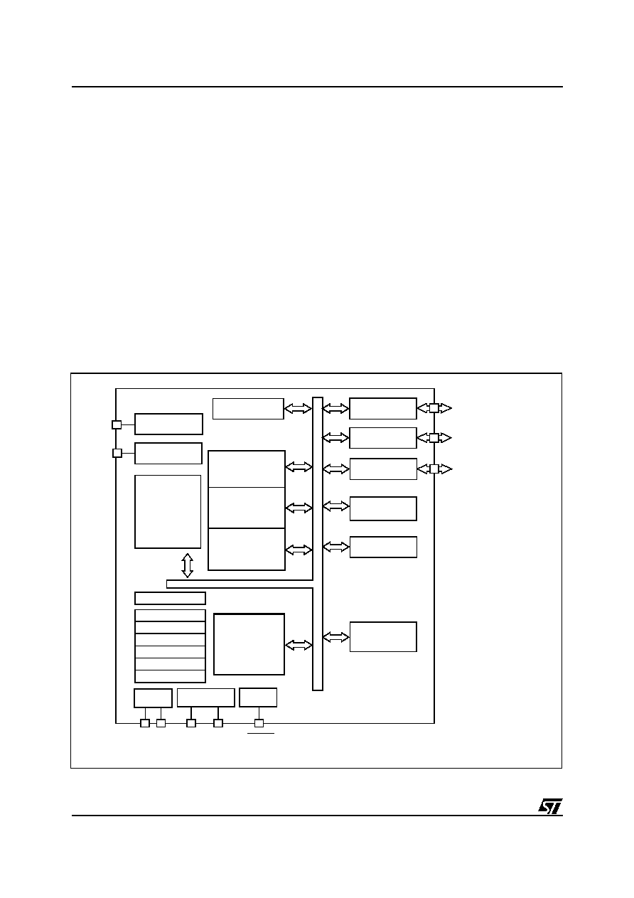
Figure 1. Block Diagram
TEST
NMI
INTERRUPT
PROGRAM
PC
STACK LEVEL 1
STACK LEVEL 2
STACK LEVEL 3
STACK LEVEL 4
STACK LEVEL 5
STACK LEVEL 6
POWER
SUPPLY
OSCILLATOR
RESET
DATA ROM
USER
SELECTABLE
DATA RAM
PORT A
PORT B
TIMER
DIGITAL
8 BIT CORE
TEST/V
PP
8-BIT
A/D CONVERTER
PA4..PA5 / Ain
PB0, PB2..PB3 / 20 mA Sink
V
DD
V
SS
OSCin OSCout
RESET
WATCHDOG
MEMORY
PB6 / ARTimin / 20 mA Sink
PORT C
PC2..PC3 / Ain
AUTORELOAD
TIMER
PB7 / ARTimout / 20 mA Sink
128 Bytes
1836 bytes OTP
(ST62T52B, T62B)
1836 bytes EPROM
(ST62E62B)
DATA EEPROM
64 Bytes
(ST62T62B/E62B)
4
5/68
ST62T52B ST62T62B/E62B
1.2 PIN DESCRIPTIONS
V
DD
and V
SS
. Power is supplied to the MCU via
these two pins. V
DD
is the power connection and
V
SS
is the ground connection.
OSCin and OSCout. These pins are internally
connected to the on-chip oscillator circuit. A quartz
crystal, a ceramic resonator or an external clock
signal can be connected between these two pins.
The OSCin pin is the input pin, the OSCout pin is
the output pin.
RESET. The active-low RESET pin is used to re-
start the microcontroller.
TEST/V
PP
. The TEST must be held at V
SS
for nor-
mal operation. If TEST pin is connected to a
+12.5V level during the reset phase, the
EPROM/OTP programming Mode is entered.
NMI. The NMI pin provides the capability for asyn-
chronous interruption, by applying an external non
maskable interrupt to the MCU. The NMI input is
falling edge sensitive. It is provided with an on-
chip pullup resistor and Schmitt trigger character-
istics.
PA4-PA5. These 2 lines are organized as one I/O
port (A). Each line may be configured under soft-
ware control as inputs with or without internal pull-
up resistors, interrupt generating inputs with pull-
up resistors, open-drain or push-pull outputs, ana-
log inputs for the A/D converter.
PB0, PB2-PB3, PB6-PB7. These 5 lines are or-
ganized as one I/O port (B). Each line may be con-
figured under software control as inputs with or
without internal pull-up resistors, interrupt gener-
ating inputs with pull-up resistors, open-drain or
push-pull outputs. PB6/ARTIMin and PB7/ARTI-
Mout are either Port B I/O bits or the Input and
Output pins of the ARTimer.
Reset state of PB2-PB3 pins can be defined by
option either with pull-up or high impedance.
PB0, PB2-PB3, PB6-PB7 scan also sink 20mA for
direct LED driving.
PC2-PC3. These 2 lines are organized as one I/O
port (C). Each line may be configured under soft-
ware control as input with or without internal pull-
up resistor, interrupt generating input with pull-up
resistor, analog input for the A/D converter, open-
drain or push-pull output.
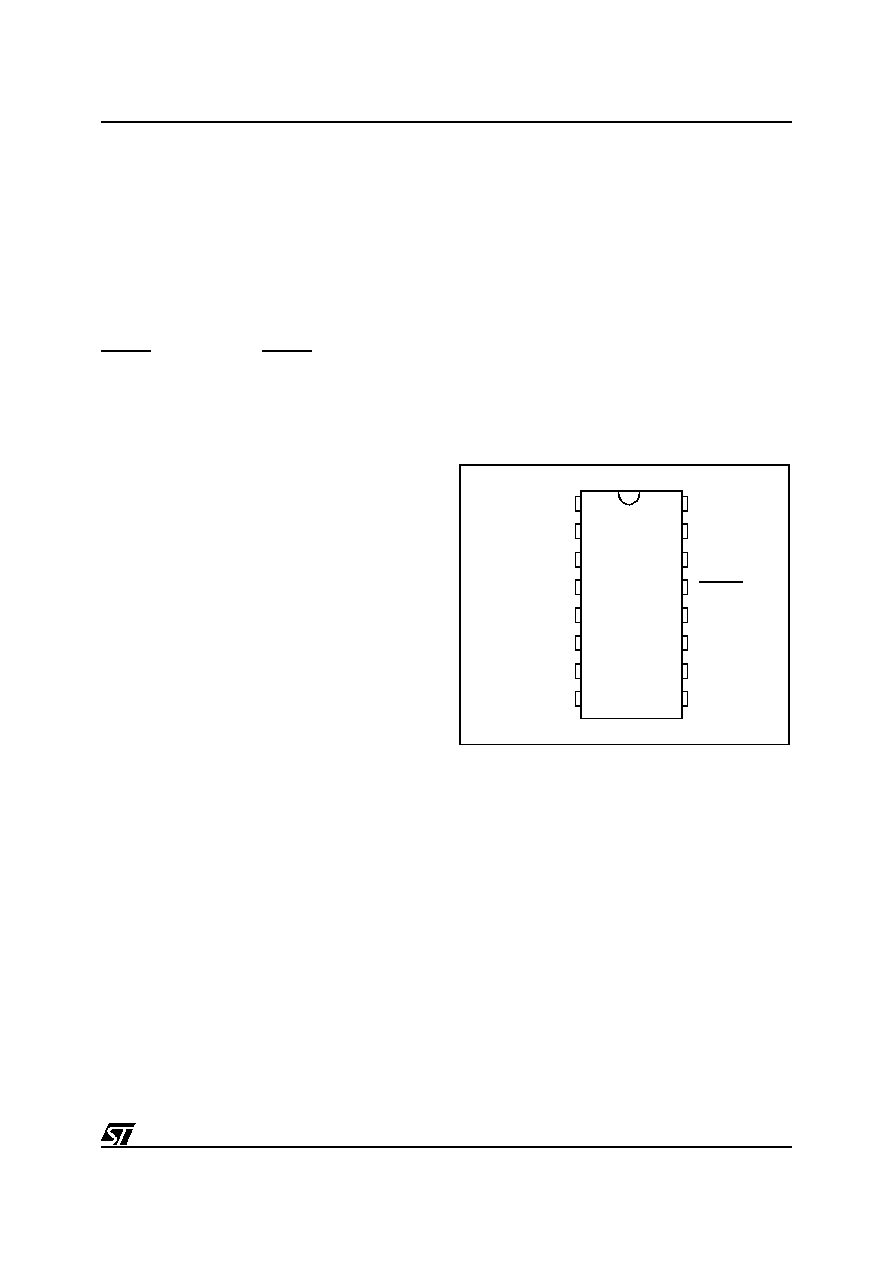
Figure 2. ST62T52B, E62B and T62B Pin
Configuration
1
2
3
4
5
6
7
8
9
10
11
12
13
14
15
16
PB0
V
PP
/TEST
PB2
PB3
V
DD
ARTIMin/PB6
PC2/Ain
PC3/Ain
PA5/Ain
PA4/Ain
ARTIMout/PB7
V
SS
NMI
RESET
OSCout
OSCin
5