1/28
October 2001
s
DMT MODEM FOR CPE ADSL,
COMPATIBLE WITH THE FOLLOWING
STANDARDS:
- ANSI T1.413 ISSUE 2
- ITU-T G.992.1 (G.DMT)
- ITU-T G.992.2 (G.LITE)
s
SUPPORTS EITHER ATM (UTOPIA LEVEL
1 & 2) OR BITSTREAM INTERFACE
s
16 BIT MULTIPLEXED MICROPROCESSOR
INTERFACE (LITTLE AND BIG ENDIAN
COMPATIBILITY)
s
ANALOG FRONT END MANAGEMENT
s
DUAL LATENCY PATHS: FAST AND
INTERLEAVED
s
ATM'S PHY LAYER: CELL PROCESSING
(CELL DELINEATION, CELL INSERTION,
HEC)
s
ADSL'S OVERHEAD MANAGEMENT
s
REED SOLOMON ENCODE/DECODE
s
TRELLIS ENCODE/DECODE (VITERBI)
s
DMT MAPPING / DEMAPPING OVER 256
CARRIERS
s
FINE (2PPM) TIMING RECOVER USING
ROTOR AND ADAPTATIVE FREQUENCY
DOMAIN EQUALIZING
s
TIME DOMAIN EQUALIZATION
s
FRONT END DIGITAL FILTERS
s
0.25
�
m HCMOS7 TECHNOLOGY
s
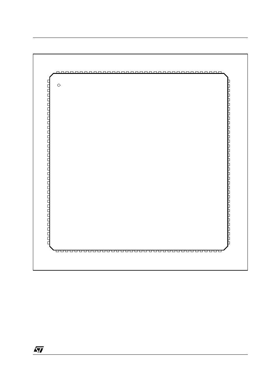
144 PIN TQFP
s
POWER CONSUMPTION: 0.4 WATT
APPLICATIONS
Routers at SOHO, stand-alone modems, PC
modems.
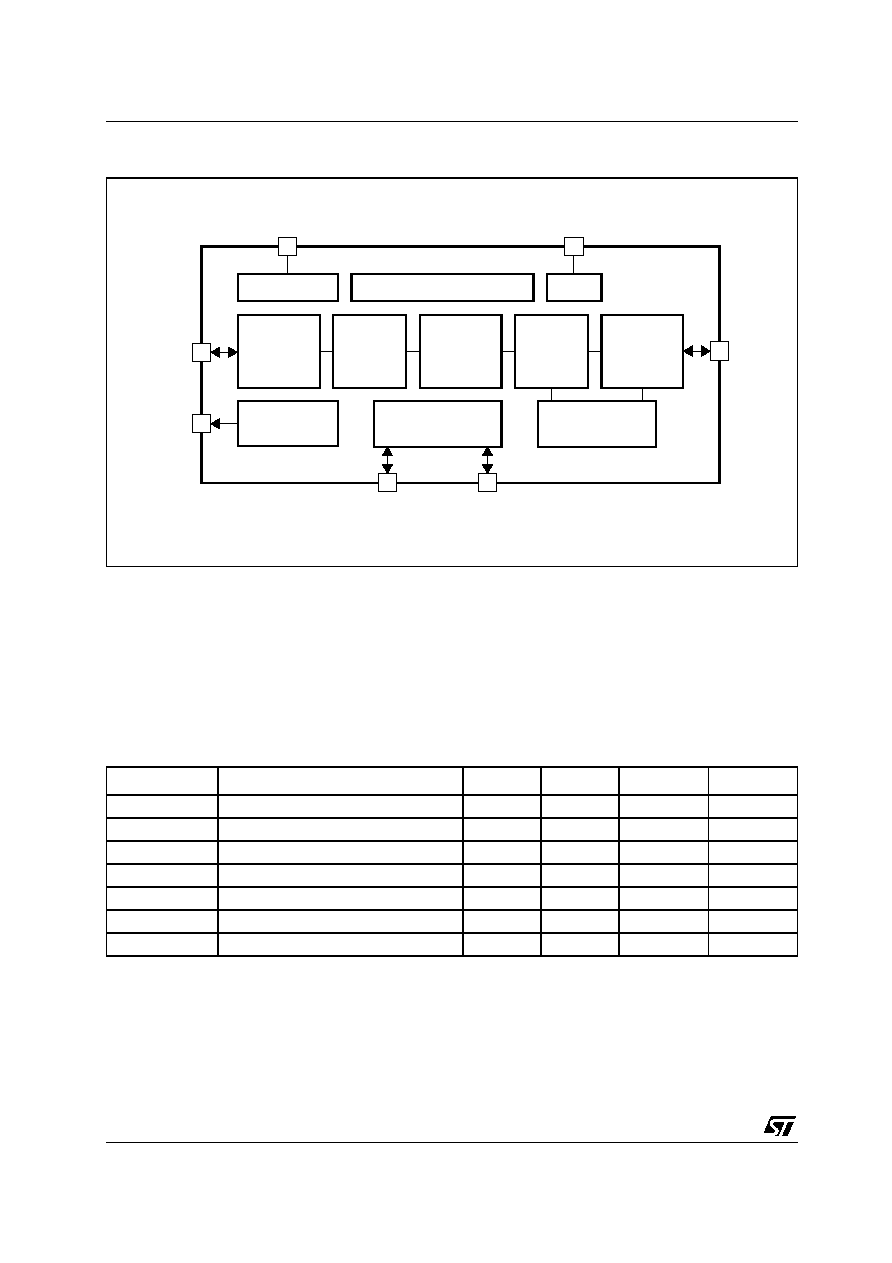
GENERAL DESCRIPTION
The ST70235A is the DMT modem and ATM
framer of the STMicroelectronics ASCOTTM
chipset. When coupled with ST70134 analog
front-end and an external controller running
dedicated firmware, the product fulfills ANSI
T1.413 "Issue 2" DMT ADSL specification. The
chip supports UTOPIA level 1 and UTOPIA level 2
interface.
The ST70235A can be split up into two different
sections. The physical one performs the
DMT modulation, demodulation, Reed-Solomon
encoding, bit interleaving and 4D trellis coding.
The ATM section embodies framing functions for
the generic and ATM Transmission Convergence
(TC) layers. The generic TC consists of data
scrambling and Reed Solomon error corrections,
with and without interleaving.
The ST70235A is controlled and programmed
by an external controller (ADSL Transceiver Con-
troller, ATC) that sets the programmable coeffi-
cients. The firmware controls the initialization
phase and carries out the consequent adaptation
operations.
TQFP144 Full Plastic
(20 x 20 x 1.40 mm)
ORDER CODE: ST70235A
ST70235A
ASCOT
TM
DMT TRANSCEIVER
This is advance information on a new product now in development or undergoing evaluation. Details are subject to change without notice.
PRELIMINARY DATA
ST70235A
2/28
Figure 1 : Block Diagram
Transient Energy Capabilities
ESD (Electronic Discharged) tests have been performed for the Human Body Model (HBM) and for the
Charged Device Model (CDM).
The pins of the device are to be able to withstand minimum 2000V for the HBM and minimum 250V for
CDM.
Latch-up
The maximum sink or source current from any pin is limited to 200mA to prevent latch-up.
ABSOLUTE MAXIMUM RATINGS
Symbol
Parameter
Min.
Typ.
Max.
Unit
V
DD
3.3
Supply Voltage
3.0
3.3
3.6
V
V
DD
1.8
Supply Voltage
1.62
1.8
1.98
V
P
tot
Total Power Dissipation
300
400
mW
T
amb
Ambient Temperature 1m/s airflow
0
70
�C
R
th
J/A
Thermal Resistivity
38
�C/W
I
3.3
Current Consumption
14
mA
I
1.8
Current Consumption
135
mA
TEST MODULE
DATA SYMBOL TIMING UNIT
VCXO
DSP
FRONT-END
FFT/IFFT
ROTOR
TRELLIS
CODING
GENERIC
TC
INTERFACE
MODULE
AFE CONTROL
CONTROLLER
ATM
TEST SIGNALS
CLOCK
AFE
INTERFACE
AFE
CONTROL
CONTROLLER
BUS
GENERAL
PURPOSE I/Os
UTOPIA
MAPPER/
DEMAPPER
REED/
SOLOMON
INTERFACE
SPECIFIC TC
INTERFACE
ST70235A
4/28
PIN FUNCTIONS
Pin Name
Type
PAD Type
HCMOS7
BS
Function
1
VSS
0V Ground
2
AD_0
B
BD8STARP
B
Data 0
3
AD_1
B
BD8STARP
B
Data 1
4
AD_2
B
BD8STARP
B
Address / Data 2
5
VDD 3.3
(VSS + 3.3V) Power Supply
6
AD_3
B
BD8STARP
B
Address / Data 3
7
AD_4
B
BD8STARP
B
Address / Data 4
8
VSS
0V Ground
9
AD_5
B
BD8STARP
B
Address / Data 5
10
AD_6
B
BD8STARP
B
Address / Data 6
11
VDD 3.3
(VSS + 3.3V) Power Supply
12
AD_7
B
BD8STARP
B
Address / Data 7
13
AD_8
B
BD8STARP
B
Address / Data 8
14
AD_9
B
BD8STARP
B
Address / Data 9
15
VSS
0V Ground
16
AD_10
B
BD8STARP
B
Address / Data 10
17
AD_11
B
BD8STARP
B
Address / Data 11
18
VDD 1.8
(VSS + 1.8V) Power Supply
19
AD_12
B
BD8STARP
B
Address / Data 12
20
VSS
0V Ground
21
PCLK
I
TLCHT
I
Processor clock
22
VDD 3.3
(VSS + 3.3V) Power Supply
23
AD_13
B
BD8STARP
B
Address / Data 13
24
AD_14
B
BD8STARP
B
Address / Data 14
25
AD_15
B
BD8STARP
B
Address / Data 15
26
VSS
0V Ground
27
BE1
I
TLCHT
I
Address 1
28
ALE
I
TLCHT
C
Address Latch
29
VDD 3.3
(VSS + 3.3V) Power Supply
30
CSB
I
TLCHT
I
Chip Select
31
WR_RDB
I
TLCHT
I
Specifies the direction of the access cycle
32
RDYB
OZ
BD4STARP
O
Controls the ATC bus cycle termination
33
OBC_TYPE
I-PD
TLCHTDQ
I
ATC Mode Selection (0 = i960; 1 = generic)
34
INTB
O
BD4STARP
O
Requests ATC interrupt service
35
RESETB
I
TLCHT
I
Hard reset
36
VSS
0V Ground
37
VDD 3.3
(VSS + 3.3V) Power Supply
38
U_RxData_0
OZ
BD8STARP
B
Utopia RX Data 0
39
U_RxData_1
OZ
BD8STARP
B
Utopia RX Data 1
40
VSS
0V Ground
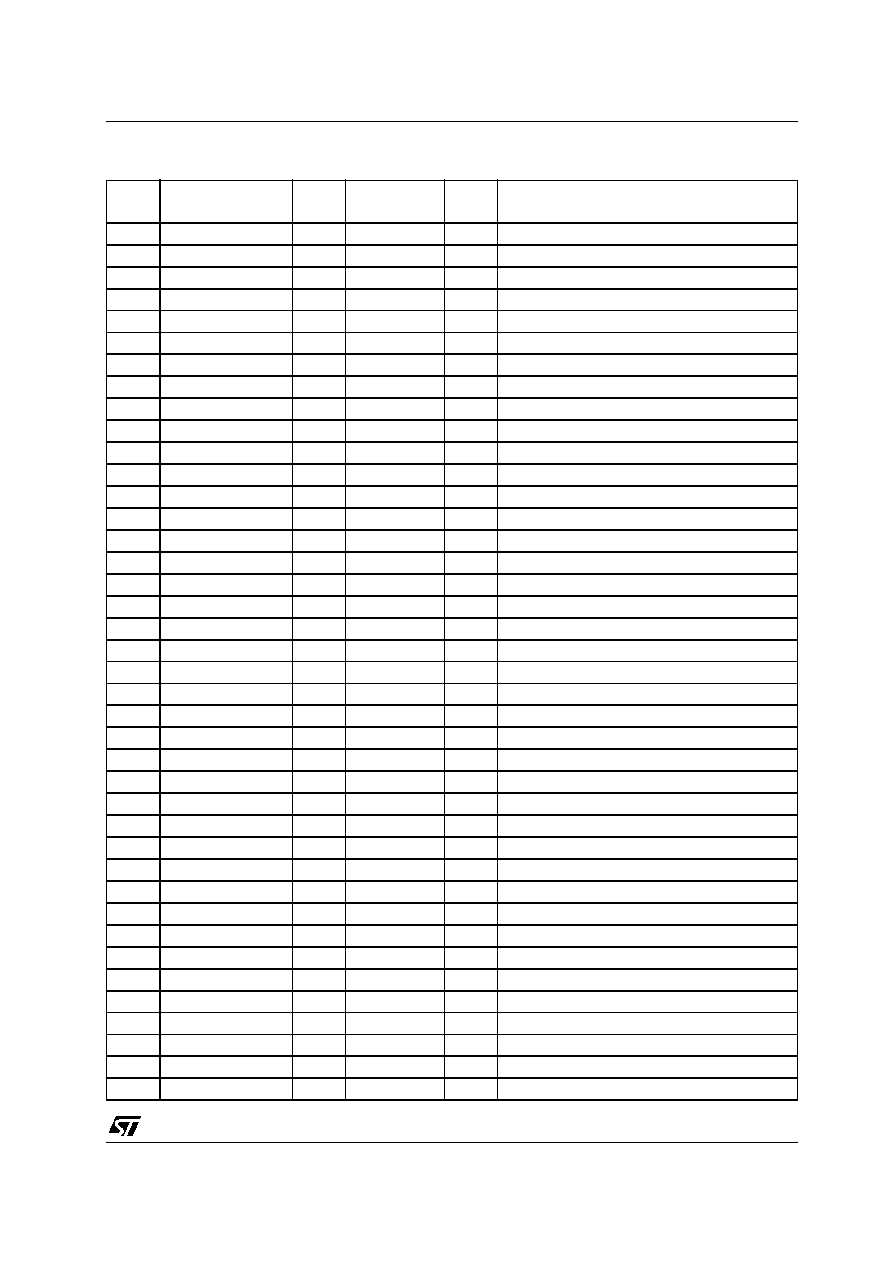
ST70235A
5/28
41
U_RxData_2
OZ
BD8STARP
B
Utopia RX Data 2
42
U_RxData_3
OZ
BD8STARP
B
Utopia RX Data 3
43
VDD 1.8
(VSS + 1.8V) Power Supply
44
U_RxData_4
OZ
BD8STARP
B
Utopia RX Data 4
45
U_RxData_5
OZ
BD8STARP
B
Utopia RX Data 5
46
VSS
0V Ground
47
U_RxData_6
OZ
BD8STARP
B
Utopia RX Data 6
48
U_RxData_7
OZ
BD8STARP
B
Utopia RX Data 7
49
VDD 3.3
(VSS + 3.3V) Power Supply
50
U_RxADDR_0
I
TLCHT
I
Utopia RX Address 0
51
U_RxADDR_1
I
TLCHT
I
Utopia RX Address 1
52
U_RxADDR_2
I
TLCHT
I
Utopia RX Address 2
53
U_RxADDR_3
I
TLCHT
I
Utopia RX Address 3
54
VSS
0V Ground
55
U_RxADDR_4
I
TLCHT
I
Utopia RX Address 4
56
GP_IN_0
I-PD
TLCHTDQ
I
General purpose input 0
57
VDD 3.3
(VSS + 3.3V) Power Supply
58
GP_IN_1
I-PD
TLCHTDQ
I
General purpose input 1
59
VSS
0V Ground
60
U_RxRefB
O
BD4STARP
O
8kHz clock to ATM device
61
U_TxRefB
I
TLCHT
I
8kHz clock from ATM device
62
VDD 1.8
(VSS + 1.8V) Power Supply
63
U_Rx_CLK
I
TLCHT
Utopia RX Clock
64
U_Rx_SOC
OZ
BD8STARP
Utopia RX Start of Cell
65
U_RxCLAV
OZ
BD8STARP
Utopia RX Cell Available
66
U_RxENBB
I
TLCHT
Utopia RX Enable
67
VSS
0V Ground
68
U_Tx_CLK
I
TLCHT
Utopia TX Clock
69
U_Tx_SOC
I
TLCHT
Utopia TX Start of Cell
70
U_TxCLAV
OZ
BD8SCR
Utopia TX Cell Available
71
U_TxENBB
I
TLCHT
Utopia TX Enable
72
VDD 3.3
(VSS + 3.3V) Power Supply
73
VSS
0V Ground
74
U_TxData_7
I
TLCHT
I
Utopia TX Data 7
75
U_TxData_6
I
TLCHT
I
Utopia TX Data 6
76
VDD 3.3
(VSS + 3.3V) Power Supply
77
U_TxData_5
I
TLCHT
I
Utopia TX Data 5
78
U_TxData_4
I
TLCHT
I
Utopia TX Data 4
79
U_TxData_3
I
TLCHT
I
Utopia TX Data 3
80
U_TxData_2
I
TLCHT
I
Utopia TX Data 2
Pin Name
Type
PAD Type
HCMOS7
BS
Function
PIN FUNCTIONS (continued)