ST7 - LOW-POWER, FULL-SPEED USB 8-BIT MCU WITH 32K FLASH, 5K RAM, FLASH CARD I/F, TIMER, PWM, ADC, I2C
June 2003
1/166
This is preliminary information on a new product. Details are subject to change without notice.
Rev. 2.3
ST7265x
LOW-POWER, FULL-SPEED USB 8-BIT MCU WITH 32K
FLASH, 5K RAM, FLASH CARD I/F, TIMER, PWM, ADC,
I
2
C, SPI
DATASHEET
s
Memories
Up to 32K of ROM or High Density Flash (HD-
Flash) program memory with read/write pro-
tection
For HDFlash devices, In-Application Pro-
gramming (IAP) via USB and In-Circuit pro-
gramming (ICP)
Up to 5 Kbytes
of RAM with up to 256 bytes
stack
s
Clock, Reset and Supply Management
PLL for generating 48 MHz USB clock using a
12 MHz crystal
Low Voltage Reset (except on E suffix devic-
es)
Dual supply management: analog voltage de-
tector on the USB power line to enable smart
power switching from USB power to battery
(on E suffix devices).
Programmable Internal Voltage Regulator for
Memory cards (2.8V to 3.5V) supplying:
Flash Card I/O lines (voltage shifting)
Up to 50 mA for Flash card supply
Clock-out capability
s
47 programmable I/O lines
15 high sink I/Os (8mA @0.6V / 20mA@1.3V)
5 true open drain outputs
24 lines programmable as interrupt inputs
s
USB (Universal Serial Bus) Interface
with DMA for full speed bulk applications com-
pliant with USB 12 Mbs specification (version
2.0 compliant)
On-Chip 3.3V USB voltage regulator and
transceivers with software power-down
5 USB endpoints:
1 control endpoint
2 IN endpoints supporting interrupt and bulk
2 OUT endpoints supporting interrupt and
bulk
Hardware conversion between USB bulk
packets and 512-byte blocks
s
Mass Storage Interface
DTC (Data Transfer Coprocessor): Universal
Serial/Parallel communications interface, with
software plug-ins for current and future proto-
col standards:
Compact Flash - Multimedia Card -
Secure Digital Card - SmartMediaCard -
Sony Memory Stick - NAND Flash -
ATA Peripherals
s
2 Timers
Configurable Watchdog for system reliability
16-bit Timer with 2 output compare functions.
s
2 Communication Interfaces
SPI synchronous serial interface
I
2
C Single Master Interface up to 400 KHz
s
D/A and A/D Peripherals
PWM/BRM Generator (with 2 10-bit PWM/
BRM outputs)
8-bit A/D Converter (ADC) with 8 channels
s
Instruction Set
8-bit data manipulation
63 basic instructions
17 main addressing modes
8 x 8 unsigned multiply instruction
True bit manipulation
s
Development Tools
Full hardware/software development package
Device Summary
TQFP64 10x10
TQFP48
SO34 shrink
Features
ST72651
ST72F651
ST72652
Program memory
32K ROM
32K FLASH
16K ROM
User RAM (stack) - bytes
5K (256)
512 (256)
Peripherals
USB, DTC, Timer, ADC, SPI, I
2
C, PWM, WDT
USB, DTC, WDT
Operating Supply
Dual 2.7V to 5.5V or
4.0V to 5.5V (for USB)
Dual 3.0V to 5.5V or
4.0V to 5.5V (for USB)
Single 4.0V to 5.5V
Package
TQFP64 (10 x10)
TQFP64 (10 x10) / TQFP48 (7x7) / SO34
Operating Temperature
0°C to +70°C
1

Table of Contents
2/166
-
1 INTRODUCTION . . . . . . . . . . . . . . . . . . . . . . . . . . . . . . . . . . . . . . . . . . . . . . . . . . . . . . . . . . . . . . 4
2 PIN DESCRIPTION . . . . . . . . . . . . . . . . . . . . . . . . . . . . . . . . . . . . . . . . . . . . . . . . . . . . . . . . . . . . 7
3 REGISTER & MEMORY MAP . . . . . . . . . . . . . . . . . . . . . . . . . . . . . . . . . . . . . . . . . . . . . . . . . . . 1 8
4 FLASH PROGRAM MEMORY . . . . . . . . . . . . . . . . . . . . . . . . . . . . . . . . . . . . . . . . . . . . . . . . . . 22
4.1 INTRODUCTION . . . . . . . . . . . . . . . . . . . . . . . . . . . . . . . . . . . . . . . . . . . . . . . . . . . . . . . . 22
4.2 MAIN FEATURES . . . . . . . . . . . . . . . . . . . . . . . . . . . . . . . . . . . . . . . . . . . . . . . . . . . . . . . 22
4.3 STRUCTURE . . . . . . . . . . . . . . . . . . . . . . . . . . . . . . . . . . . . . . . . . . . . . . . . . . . . . . . . . . . 22
4.4 PROGRAM MEMORY READ-OUT PROTECTION . . . . . . . . . . . . . . . . . . . . . . . . . . . . . . 22
4.5 ICP (IN-CIRCUIT PROGRAMMING) . . . . . . . . . . . . . . . . . . . . . . . . . . . . . . . . . . . . . . . . . 23
4.6 IAP (IN-APPLICATION PROGRAMMING) . . . . . . . . . . . . . . . . . . . . . . . . . . . . . . . . . . . . . 24
4.7 RELATED DOCUMENTATION . . . . . . . . . . . . . . . . . . . . . . . . . . . . . . . . . . . . . . . . . . . . . 24
4.8 REGISTER DESCRIPTION . . . . . . . . . . . . . . . . . . . . . . . . . . . . . . . . . . . . . . . . . . . . . . . . 24
5 CENTRAL PROCESSING UNIT . . . . . . . . . . . . . . . . . . . . . . . . . . . . . . . . . . . . . . . . . . . . . . . . . 25
5.1 INTRODUCTION . . . . . . . . . . . . . . . . . . . . . . . . . . . . . . . . . . . . . . . . . . . . . . . . . . . . . . . . 25
5.2 MAIN FEATURES . . . . . . . . . . . . . . . . . . . . . . . . . . . . . . . . . . . . . . . . . . . . . . . . . . . . . . . 25
5.3 CPU REGISTERS . . . . . . . . . . . . . . . . . . . . . . . . . . . . . . . . . . . . . . . . . . . . . . . . . . . . . . . 25
6 SUPPLY, RESET AND CLOCK MANAGEMENT . . . . . . . . . . . . . . . . . . . . . . . . . . . . . . . . . . . . 28
6.1 CLOCK SYSTEM . . . . . . . . . . . . . . . . . . . . . . . . . . . . . . . . . . . . . . . . . . . . . . . . . . . . . . . . 28
6.2 RESET SEQUENCE MANAGER (RSM) . . . . . . . . . . . . . . . . . . . . . . . . . . . . . . . . . . . . . . 29
6.3 LOW VOLTAGE DETECTOR (LVD) . . . . . . . . . . . . . . . . . . . . . . . . . . . . . . . . . . . . . . . . . 32
6.4 POWER SUPPLY MANAGEMENT . . . . . . . . . . . . . . . . . . . . . . . . . . . . . . . . . . . . . . . . . . 33
7 INTERRUPTS . . . . . . . . . . . . . . . . . . . . . . . . . . . . . . . . . . . . . . . . . . . . . . . . . . . . . . . . . . . . . . . 41
7.1 INTRODUCTION . . . . . . . . . . . . . . . . . . . . . . . . . . . . . . . . . . . . . . . . . . . . . . . . . . . . . . . . 41
7.2 MASKING AND PROCESSING FLOW . . . . . . . . . . . . . . . . . . . . . . . . . . . . . . . . . . . . . . . 41
7.3 INTERRUPTS AND LOW POWER MODES . . . . . . . . . . . . . . . . . . . . . . . . . . . . . . . . . . . 43
7.4 CONCURRENT & NESTED MANAGEMENT . . . . . . . . . . . . . . . . . . . . . . . . . . . . . . . . . . 43
7.5 INTERRUPT REGISTER DESCRIPTION . . . . . . . . . . . . . . . . . . . . . . . . . . . . . . . . . . . . . 44
8 POWER SAVING MODES . . . . . . . . . . . . . . . . . . . . . . . . . . . . . . . . . . . . . . . . . . . . . . . . . . . . . 47
8.1 INTRODUCTION . . . . . . . . . . . . . . . . . . . . . . . . . . . . . . . . . . . . . . . . . . . . . . . . . . . . . . . . 47
8.2 WAIT MODE . . . . . . . . . . . . . . . . . . . . . . . . . . . . . . . . . . . . . . . . . . . . . . . . . . . . . . . . . . . 47
8.3 HALT MODE . . . . . . . . . . . . . . . . . . . . . . . . . . . . . . . . . . . . . . . . . . . . . . . . . . . . . . . . . . . 48
9 I/O PORTS . . . . . . . . . . . . . . . . . . . . . . . . . . . . . . . . . . . . . . . . . . . . . . . . . . . . . . . . . . . . . . . . . . 49
9.1 INTRODUCTION . . . . . . . . . . . . . . . . . . . . . . . . . . . . . . . . . . . . . . . . . . . . . . . . . . . . . . . . 49
9.2 FUNCTIONAL DESCRIPTION . . . . . . . . . . . . . . . . . . . . . . . . . . . . . . . . . . . . . . . . . . . . . . 49
9.3 I/O PORT IMPLEMENTATION . . . . . . . . . . . . . . . . . . . . . . . . . . . . . . . . . . . . . . . . . . . . . . 53
9.4 REGISTER DESCRIPTION . . . . . . . . . . . . . . . . . . . . . . . . . . . . . . . . . . . . . . . . . . . . . . . . 54
10 MISCELLANEOUS REGISTERS . . . . . . . . . . . . . . . . . . . . . . . . . . . . . . . . . . . . . . . . . . . . . . . 56
11 ON-CHIP PERIPHERALS . . . . . . . . . . . . . . . . . . . . . . . . . . . . . . . . . . . . . . . . . . . . . . . . . . . . . 58
11.1 WATCHDOG TIMER (WDG) . . . . . . . . . . . . . . . . . . . . . . . . . . . . . . . . . . . . . . . . . . . . . . . 58
11.2 DATA TRANSFER COPROCESSOR (DTC) . . . . . . . . . . . . . . . . . . . . . . . . . . . . . . . . . . . 61
11.3 USB INTERFACE (USB) . . . . . . . . . . . . . . . . . . . . . . . . . . . . . . . . . . . . . . . . . . . . . . . . . . 65
11.4 16-BIT TIMER . . . . . . . . . . . . . . . . . . . . . . . . . . . . . . . . . . . . . . . . . . . . . . . . . . . . . . . . . . 80
1

Table of Contents
3/166
11.5 PWM/BRM GENERATOR (DAC) . . . . . . . . . . . . . . . . . . . . . . . . . . . . . . . . . . . . . . . . . . . . 92
11.6 SERIAL PERIPHERAL INTERFACE (SPI) . . . . . . . . . . . . . . . . . . . . . . . . . . . . . . . . . . . . 98
11.7 I²C SINGLE MASTER BUS INTERFACE (I2C) . . . . . . . . . . . . . . . . . . . . . . . . . . . . . . . . 109
11.8 8-BIT A/D CONVERTER (ADC) . . . . . . . . . . . . . . . . . . . . . . . . . . . . . . . . . . . . . . . . . . . . 118
12 INSTRUCTION SET . . . . . . . . . . . . . . . . . . . . . . . . . . . . . . . . . . . . . . . . . . . . . . . . . . . . . . . . 122
12.1 CPU ADDRESSING MODES . . . . . . . . . . . . . . . . . . . . . . . . . . . . . . . . . . . . . . . . . . . . . . 122
12.2 INSTRUCTION GROUPS . . . . . . . . . . . . . . . . . . . . . . . . . . . . . . . . . . . . . . . . . . . . . . . . 125
13 ELECTRICAL CHARACTERISTICS . . . . . . . . . . . . . . . . . . . . . . . . . . . . . . . . . . . . . . . . . . . . 128
13.1 PARAMETER CONDITIONS . . . . . . . . . . . . . . . . . . . . . . . . . . . . . . . . . . . . . . . . . . . . . . 128
13.2 ABSOLUTE MAXIMUM RATINGS . . . . . . . . . . . . . . . . . . . . . . . . . . . . . . . . . . . . . . . . . . 129
13.3 OPERATING CONDITIONS . . . . . . . . . . . . . . . . . . . . . . . . . . . . . . . . . . . . . . . . . . . . . . . 130
13.4 SUPPLY CURRENT CHARACTERISTICS . . . . . . . . . . . . . . . . . . . . . . . . . . . . . . . . . . . 132
13.5 CLOCK AND TIMING CHARACTERISTICS . . . . . . . . . . . . . . . . . . . . . . . . . . . . . . . . . . 135
13.6 MEMORY CHARACTERISTICS . . . . . . . . . . . . . . . . . . . . . . . . . . . . . . . . . . . . . . . . . . . 136
13.7 EMC CHARACTERISTICS . . . . . . . . . . . . . . . . . . . . . . . . . . . . . . . . . . . . . . . . . . . . . . . 137
13.8 I/O PORT PIN CHARACTERISTICS . . . . . . . . . . . . . . . . . . . . . . . . . . . . . . . . . . . . . . . . 142
13.9 CONTROL PIN CHARACTERISTICS . . . . . . . . . . . . . . . . . . . . . . . . . . . . . . . . . . . . . . . 146
13.10TIMER PERIPHERAL CHARACTERISTICS . . . . . . . . . . . . . . . . . . . . . . . . . . . . . . . . . 148
13.11COMMUNICATION INTERFACE CHARACTERISTICS . . . . . . . . . . . . . . . . . . . . . . . . 149
13.128-BIT ADC CHARACTERISTICS . . . . . . . . . . . . . . . . . . . . . . . . . . . . . . . . . . . . . . . . . . 154
14 PACKAGE CHARACTERISTICS . . . . . . . . . . . . . . . . . . . . . . . . . . . . . . . . . . . . . . . . . . . . . . 156
14.1 PACKAGE MECHANICAL DATA . . . . . . . . . . . . . . . . . . . . . . . . . . . . . . . . . . . . . . . . . . . 156
15 DEVICE CONFIGURATION AND ORDERING INFORMATION . . . . . . . . . . . . . . . . . . . . . . . 159
15.1 OPTION BYTE . . . . . . . . . . . . . . . . . . . . . . . . . . . . . . . . . . . . . . . . . . . . . . . . . . . . . . . . 159
15.2 DEVICE ORDERING INFORMATION AND TRANSFER OF CUSTOMER CODE . . . . . 160
15.3 DEVELOPMENT TOOLS . . . . . . . . . . . . . . . . . . . . . . . . . . . . . . . . . . . . . . . . . . . . . . . . . 162
15.4 ST7 APPLICATION NOTES . . . . . . . . . . . . . . . . . . . . . . . . . . . . . . . . . . . . . . . . . . . . . . 163
16 SUMMARY OF CHANGES . . . . . . . . . . . . . . . . . . . . . . . . . . . . . . . . . . . . . . . . . . . . . . . . . . . 165
1
ST7265x
4/166
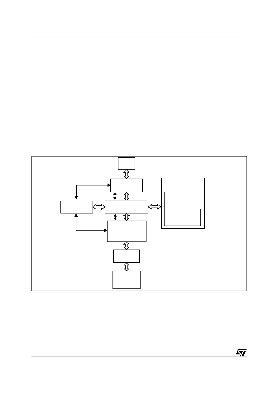
1 INTRODUCTION
The ST7265x MCU supports volume data ex-
change with a host (computer or kiosk) via a full
speed USB interface. The MCU is capable of han-
dling various transfer protocols, with a particular
emphasis on mass storage applications.
ST7265x is compliant with the USB Mass Storage
Class specifications, and supports related proto-
cols such as BOT (Bulk Only Transfer) and CBI
(Control, Bulk, Interrupt).
It is based on the ST7 standard 8-bit core, with
specific peripherals for managing USB full speed
data transfer between the host and most types of
FLASH media card:
A full speed USB interface with Serial Interface
Engine, and on-chip 3.3V regulator and trans-
ceivers.
A dedicated 24 MHz Data Buffer Manager state
machine for handling 512-byte data blocks (this
size corresponds to a sector both on computers
and FLASH media cards).
A Data Transfer Coprocessor (DTC), able to
handle fast data transfer with external devices.
This DTC also computes the CRC or ECC re-
quired to handle Mass storage media.
An Arbitration block gives the ST7 core priority
over the USB and DTC when accessing the Data
Buffer. In USB mode, the USB interface is serv-
iced before the DTC.
A FLASH Supply Block able to provide program-
mable supply voltage and I/O electrical levels to
the FLASH media.
Figure 1. USB Data Transfer Block Diagram
512-byte RAM
Buffer
512-byte RAM
Buffer
DATA
COPROCESSOR
DATA TRANSFER
BUFFER
LEVEL
SHIFTERS
MASS
DEVICE
USB
SIE
ST7 CORE
STORAGE
TRANSFER
(DTC)
ARBITRATION
USB DATA
TRANSFER
BUFFER ACCESS
1
ST7265x
5/166
INTRODUCTION (Cont'd)
In addition to the peripherals for USB full speed
data transfer, the ST7265x includes all the neces-
sary features for stand-alone applications with
FLASH mass storage.
Low voltage reset ensuring proper power-on or
power-off of the device (not on all products)
Digital Watchdog
16-bit Timer with 2 output compare functions (not
on all products - see device summary).
Two 10-bit PWM outputs (not on all products -
see device summary)
Serial Peripheral interface (not on all products -
see device summary)
Fast I
2
C Single Master interface (not on all prod-
ucts - see device summary)
8-bit Analog-to-Digital converter (ADC) with 8
multiplexed analog inputs (not on all products -
see device summary)
The ST72F65x are the Flash versions of the
ST7265x in a TQFP64 package.
The ST7265x are the ROM versions in a TQFP64
package.
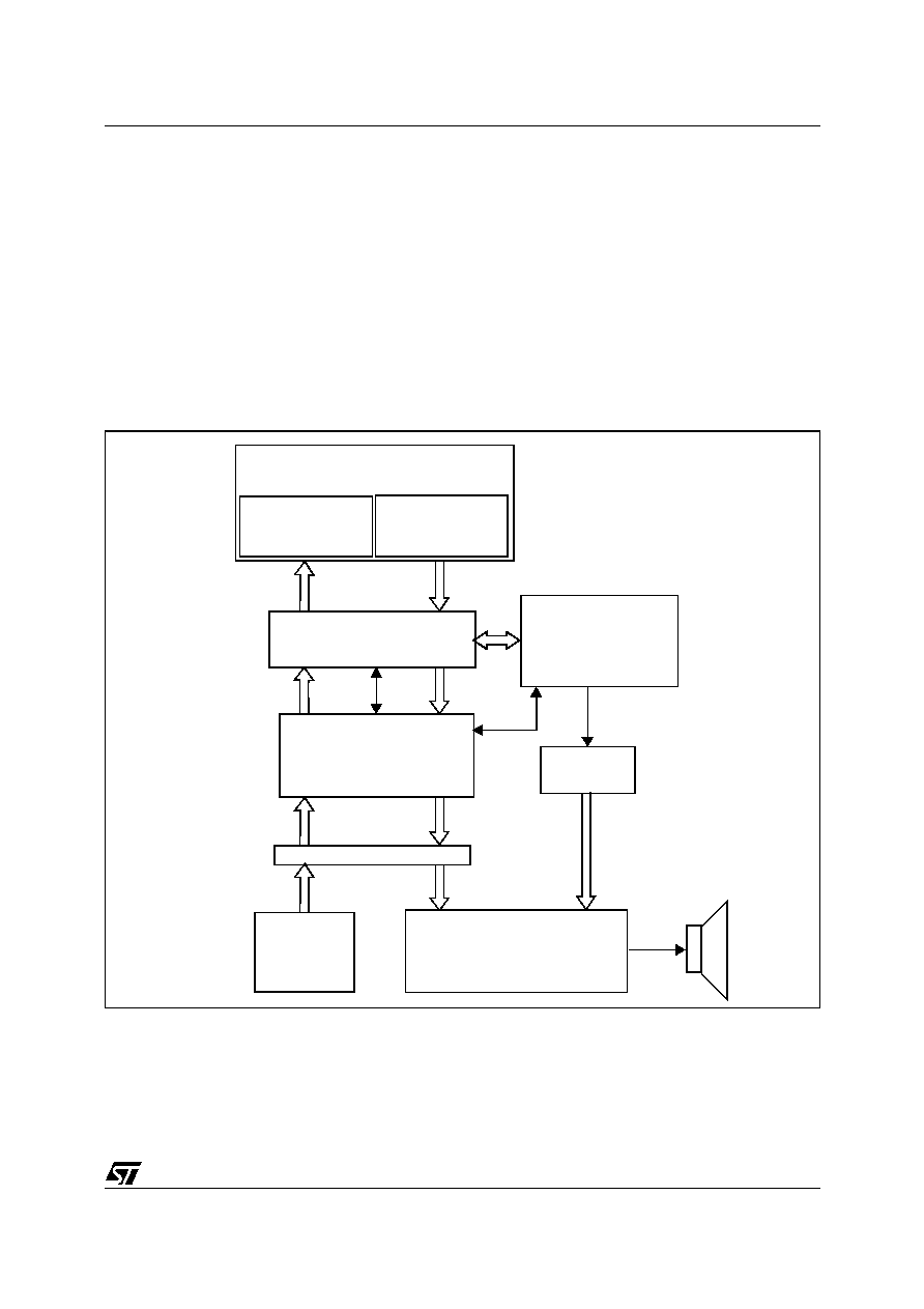
Figure 2. Digital Audio Player Application Example in Play Mode
512-byte RAM
Buffer
512-byte RAM
Buffer
DATA
COPROCESSOR
DATA TRANSFER
BUFFER
LEVEL SHIFTERS
MASS
DEVICE
ST7 CORE
STORAGE
TRANSFER
(DTC)
ARBITRATION
BUFFER ACCESS
DIGITAL
AUDIO DEVICE
I2C
1
Document Outline