 | –≠–ª–µ–∫—Ç—Ä–æ–Ω–Ω—ã–π –∫–æ–º–ø–æ–Ω–µ–Ω—Ç: ST7282 | –°–∫–∞—á–∞—Ç—å:  PDF PDF  ZIP ZIP |
PRELIMINARY DATASHEET
Family
Issuer Ref.
Chrono
March 26, 1997
Previous Ref
Edition
ST7
PG-RO
97115
7282A5B5
Target C
Page 1/23
ST7282A5 - ST7282B5
ROM FROM EPROM
s
ST72-Core
s
Controller/Driver for max. 20
◊
16, 28
◊
8
or 32
◊
4
s
LCD segments (ST7LCD4)
s
56 bytes LCD-RAM
s
864 bytes data RAM
s
512 bytes EEPROM (eep2a)
s
32Kbytes program ROM
s
24 digital I/O (ST7 IO3) with pull up,
interrupt input, analog input, push-pull/
open drain output
s
36 LCD/IO combi pins (ST7 LCIO1) with
pull-up, interrupt input, push-pull, open
drain output, LCD output
s
16 bit reload timer (ST7TIM4)
s
Watchdog Timer (ST7 WD2)
s
8 bit synchronous serial I/O (ST7SIO)
s
8 bit A/D Converter (ST7ADC2)
s
RDS Demodulator (ST7 RDS BD)
s
Group & Block Sync Module for RDS (ST7
RDS GB)
s
RDS filter (ST7 RDS FI)
s
LCD Synchro IN / Out
s
System Frequency 8.55 MHz
n
n
ST7282A5 - ST7282B5 - ROM FROM EPROM
Family
Issuer Ref.
Chrono
March 26, 1997
Previous Ref
Edition
ST7
PG-RO
97115
7282A5B5
Target C
Page 2/23
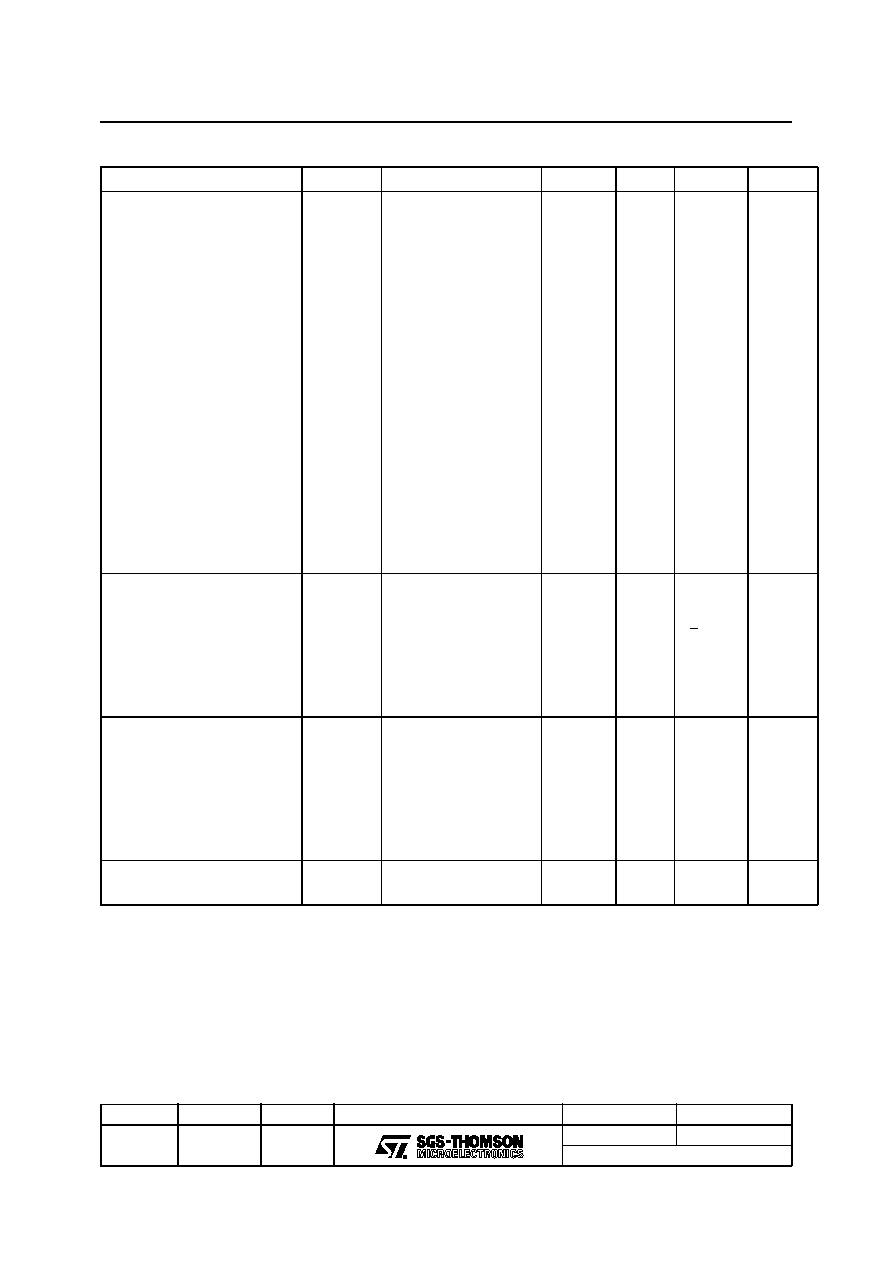
1 GENERAL DESCRIPTION
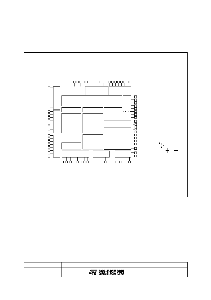
Figure 1. Block Diagram
n
n
n
W A T C H D O G
R A M 8 6 4
E E P R O M 51 2
T IM E R 1 6 b it
A D C
3 2K R O M
S T 7 2 C O R E
O S C IL L A T O R
R D S D E M O D .
G R P & B LK S Y N C
PB
7
/
AI
N
PB
6
/
AI
N
PB
5
/
AI
N
PB
4
/
AI
N
PB
3
/
AI
N
PB
2
/
AI
N
PB
1
/
AI
N
PB
0
/
AI
N
P O R T B
V
DDP
VS
SP
V
DDA
VS
SA
PC
0
/
AI
N
PC
1
/
AI
N
PC
2
/
AI
N
PC
3
/
AI
N
PC
4
/
AI
N
PC
5
/
AI
N
PC
6
/
AI
N
PC
7
/
AI
N
P O R T C
PO
R
T
A
P A 0 /C P 1/A IN
P A 7 /A IN
P A 6 /A IN
P A 5 /A IN
P A 4 /A IN
P A 3 /A IN
P A 2 /A IN
P A 1 /C P 2/A IN
O S C IN
O S C O U T /S T O P
R D S F IL
S IO
M P X
R D S C O M P /P E 4 /S 2 1
S
e
g
.
Dr
v
.
P
O
R
T
D
S 1 6 /P D 7
S 1 5 /P D 6
S 1 4 /P D 5
S 1 3 /P D 4
S 1 2 /P D 3
S 1 1 /P D 2
S 1 0 /P D 1
S 9 /P D 0
S
e
g
.
D
r
v
.
P
O
RT
F
S 8 /P F 7
S 7 /P F 6
S 6 /P F 5
S 5 /P F 4
S 4 /P F 3
S 3 /P F 2
S 2 /P F 1
S 1 /P F 0
S
e
g
.
D
r
v
.
P
O
RT
G
B P 1 6 /S 0 /P G 7
B P 1 5 /S - 1/P G 6
B P 1 4 /S - 2/P G 5
B P 1 3 /S - 3/P G 4
B P 1 2 /S - 4/P G 3
B P 1 1 /S - 5/P G 2
B P 1 0 /S - 6/P G 1
B P 9 /S -7 /P G 0
8 .5 5 M H z
S T 7 IO 3
S T 7 IO 3
ST
7
I
O
3
R D S F ilte r
R D S R E F
S T 7 R D S F I
P O R T H
BP
8
/
S-
9
/
PH
7
BP
7
/
S-
1
0
/
P
H
6
BP
6
/
S-
1
1
/
P
H
5
BP
5
/
S-
1
2
/
P
H
4
BP
4
/
PH
3
BP
3
/
PH
2
BP
2
/
PH
1
BP
1
/
PH
0
S T 7 L C IO
S T 7 O S C IL L A T O R
S T 7 R D S G B
S T 7 R D S B D
S T 7 T IM 4
S T 7 W D 2
S
T
7 LC
IO
S
T
7 LC
IO
S
T
7 LC
IO
S T 7 A D C 2
O s c - O p tio n
V D D
V S S
V P P /T E S T
L C D R A M
5 6B y te
VL
C
D
VL
C
D
4
/
5
VL
C
D
3
/
5
VL
C
D
2
/
5
VL
C
D
1
/
5
L C D C O N T R O L
S T7 L C D 4
S
1
7
/
PE0
S
1
8
/
PE1
S
1
9
/
PE2
S
2
0
/
PE3
S e g . D rv ./P o r t E
S T 7 L C IO
R E S E T
S 2 2 /P E 5
S 2 1 /P E 4 /R D S C O M P
ST7282A5 - ST7282B5 - ROM FROM EPROM
Family
Issuer Ref.
Chrono
March 26, 1997
Previous Ref
Edition
ST7
PG-RO
97115
7282A5B5
Target C
Page 3/23
1.1 Quick Reference
The ST7282A5/B5 is a 32K ROM version of the
ST72 family, using the ST72CORE and N-Well
technology.
It is derived from EPROM M4 version replacing
EPROM by ROM.
Two different commercial products are supported
by this device : ST7282A5 (no LCD driver) func-
tionnality described in specification SD70KL1618
ed. F) and ST7282B5 (LCD driver) functionnality
described in specification 96096 ed. B).
It contains an LCD controller/driver with 20 seg-
ment and 16 backplane outputs able to drive up to
20 x 16 = 320 segments.
The LCD control logic reads automatically data
from the LCD-RAM independently from the
ST7282 B5.
Further it contains up to 62 I/O pins, 24 of them
can be used as analog inputs to the 8 bit analog-
digital converter. Each digital I/O pin can individu-
ally be defined by software to work in one of the
following modes: open-drain output, push pull out-
put, input, input with pull-up (23 pins only) or inter-
rupt input with pull up (23 pins only). 3 of the digital
I/O pins serve as interface to the SIO. On pin PA4
the pull-up resistor is desactivated.
Port pins PD, PE, PF, PG and PH are multiplexed
with LCD Segment and backplane pins.
A 512 byte EEPROM for non volatile storage of
data is available. The programming voltage for
that device is generated on chip without external
components. So no extra supply is necessary. 16
bytes are protected against external readout.
One interrupt vector is connected to the I/O ports.
Five more interrupt vectors are available for the
timer, the ADC, the serial I/O interface and the
Group & Block Sync module (2). The watchdog
can be set by the user in 64 increments from
2.8msec to 182msec ( f
OSC
= 8.55 MHz ).
A synchronous 8 bit serial interface for serial data
IN/OUT is also implemented.
RDS signals can be decoded with the help of RDS
filter, RDS demodulator and Group & Block Sync
module.
1.2 Parameters
The values below substitute the corresponding values in the specifications of dedicated functions.
1.2.1 Absolute maximum ratings
1.2.2 Recommended operating conditions
The maximum accumulated current of all I/O pins
should not exceed 40 mA for V
DDP
and 40 mA for
V
SSP
.
* except LCD pins
** MIL 883B Mode, 100pF through 1.5k
Supply voltage
( V
DD
- V
SS
)
-0.3 ... +7V
Input voltage*
V
IN
V
SS
-0.3V...V
DD
+0.3V
Output voltage*
V
OUT
V
SS
-0.3V ... V
DD
+0.3V
Input current
I
in
-10 ... +10mA
Output current*
I
OUT
-10 ... + 10mA
Power dissipation
P
D
tbd
Storage temperature
T
stg
-55 ... +125∞C
Operation temperature
T
amb
-40 ... +85∞C
Display voltage
(V
LCD
- V
SS
)
V
DD
... 7V
Output voltage Seg+COM
V
OUT
V
SS
-0.3V ... V
LCD
+0.3V
ESD ESD
2500V
LU susceptibility
LU
V
DDA
, Pin 52 - Class C
Supply voltage
(V
DD
- V
SS
)
4.5 ... 5.5V
Supply votage difference
(V
DD
, V
DDP
, V
DDA
)
(V
SS
, V
SSP
, V
SSA
)
50mV
ST7282A5 - ST7282B5 - ROM FROM EPROM
Family
Issuer Ref.
Chrono
March 26, 1997
Previous Ref
Edition
ST7
PG-RO
97115
7282A5B5
Target C
Page 4/23
1.2.3 Electrical Characteristics
The values given in the specifications of dedicated functions are generally not applicable for chips. There-
fore, only the limits listed below are valid for the product. T = -40 ... +85∞C, V
DD
- V
SS
= 5V unless otherwise
specified.
PARAMETER
SYMBOL
CONDITION
MIN
TYP
MAX
UNIT
Supply voltage
V
DD
4.5
-
5.5
V
Supply current Run Mode
I
DD
f
OSC
=8.55MHz
no output load
-
10
20
mA
Supply current Wait Mode
I
DD
f
OSC
=8.55MHz
WD, Timer, LCD active
-
3
5
mA
Supply current slow wait mode
I
DD
no output load
-
0.7
2
mA
Supply current halt mode
I
DD
no output load
-
-
100
µA
Supply current Reset Mode
I
DD
V
RESET
=V
SS
f=8.55MHz
-
10
15
mA
Display voltage
V
LCD
V
DD
-
7
V
Supply voltage differences
(V
DD
, V
DDP
, V
DDA
)
(V
SS
, V
SSP
, V
SSA
)
V
D
-
-
50
mV
OSCILLATOR:
Input/output cap Cin, Cout
Oscillation frequency
1)
Built up time
2)
f
OSC
t
BU
V
DD
= 4.5V
V
DD
=5.0V
C
1
=C
2
=22pF
8.55
-
8.55
8
9.00
8.55
20
pF
MHz
ms
RESET:
Input current
3)
Input current
4)
Input current
5)
Input voltage high
Input voltage low
-I
R
I
R
I
R
V
R
V
R
Crystal
V
R
=V
SS
V
R
=V
DD
V
R
=V
DD
-
-
-
0.7V
DD
+50
+10
-
-
-
+100
+20
1
-
0.2V
DD
µA
µA
mA
V
V
POWER-ON RESET
Supply rise time
Supply recovery time
6)
Trigger level on
Trigger level off
t
r
t
rec
V
tlon
V
tloff
10%-90%
.01
10
1.4
-
-
-
.-
-
10
-
-
3
ms
ms
V
V
RDS FILTER:
Center frequency
3dB Bandwith
Gain
Attenuation
Input impedance
Load impedance
MPX input signal
fc
BW
G
A
R
I
R
L
V
IN
V
in
= 3mV
RMS
57 KHz, V
in
= 3mV
RMS
f = ±4 KHz
f = 38 KHz
f = 67 KHz
56.5
2.5
18
18
50
35
100
1
170
57
3
20
22
80
50
160
-
250
57.5
3.5
22
-
-
-
200
-
600
KHz
KHz
dB
dB
dB
dB
K
M
mV
RMS
ST7282A5 - ST7282B5 - ROM FROM EPROM
Family
Issuer Ref.
Chrono
March 26, 1997
Previous Ref
Edition
ST7
PG-RO
97115
7282A5B5
Target C
Page 5/23
1)Operation below 30 KHz Mis possible but requires increased supply current
2)Time to build up the oscillation amplitude to 90% V
DD
3)Pull-up resistor
4)WD not active
5)WD generating a reset
6)Period for which V
DD
has to be disconnected or at OV to allow internal reset function at next power
up
7)pull up off
I/O PORTS:
Input leakage current
7)
Input leakage current
Input voltage high
Input voltage low
Output voltage high
(PA,PB,PC)
Output voltage high
(PD, PE, PF, PG, PH)
Output voltage low
(PA, PB, PC, PD, PE, PF, PG,
PH)
Output voltage slope
Output current slope
Noise amplitude
Pullup Resistor Current
I
IL
I
IH
V
IH
V
IL
V
OH
V
OH
V
OH
V
OH
V
OL
V
OL
dV
O
/dt
dI
O
/dt
V
N
I
RPU
V=V
SS
V=V
DD
leading edge
trailing edge
I=5mA, V
DD
=4.5V
I=1.0mA, V
DD
=4.5V
I=2.5mA, V
DD
=4.5V
I=0.5mA, V
DD
=4.5V
I=-5mA, V
DD
=4.5V
I=-1.6mA, V
DD
=4.5V
C
L
=50pF
C
L
=50pF
20MHz-250MHz
V
IN
=V
SS
-
-
0.7V
DD
-
3.0
4.1
3.0
4.1
-
-
-
-
-
-
-
-
-
-
-
-
-
-
-
-
-
0.25
2.5
100
-
50
10
10
-
0.2V
DD
-
-
-
-
1.0
0.4
-
-
-
-
-
µ
A
µ
A
V
V
V
V
V
V
V
V
V/ns
mA/ns
µ
V
-
µA
ADC:
Resolution
Total Error
Conversion time
Input capacitance
Analog source impedance
Osc. frequency range
V
A1
t
con
R
VA
f
OSC
=8.55MHz
8)
f
OSC
=8.55MHz
8)
f
OSC
=8.55MHz
-
-
34
-
-
8.55
-
+2
35
5
30
-
bit
LSB
µ
s
pF
K
MHz
LCD DRIVER:
Frame frequency
DC offset voltage
9)
COM output voltage high
COM output voltage low
SEG output voltage high
SEG output voltage low
f
F
V
OS
V
OH
V
OL
V
OH
V
OL
f
OSC
=8.55MHz
V
LCD
=V
DD
, no load
I=50
µ
A
I=50
µ
A
I=25
µ
A
I=25
µ
A
-
-
-
-
-
-
132
50
-
0.5
-
0.5
Hz
mV
V
V
V
V
EEPROM:
Write time
t
W
V
DD
=4.5V
-
10
ms
PARAMETER
SYMBOL
CONDITION
MIN
TYP
MAX
UNIT