Rev. 4.0
September 2005
1/140
ST7263B
LOW SPEED USB 8-BIT MCU FAMILY WITH UP TO 32K FLASH/ROM,
DFU CAPABILITY, 8-BIT ADC, WDG, TIMER, SCI & I≤C
Memories
≠ 4, 8, 16 or 32 Kbytes Program Memory: High
Density Flash (HDFlash), FastROM or ROM
with Readout and Write Protection
≠ In-Application Programming (IAP) and In-Cir-
cuit programming (ICP)
≠ 384, 512 or 1024 bytes RAM memory (128-
byte stack)
Clock, Reset and Supply Management
≠ Run, Wait, Slow and Halt CPU modes
≠ 12 or 24 MHz Oscillator
≠ RAM Retention mode
≠ Optional Low Voltage Detector (LVD)
USB (Universal Serial Bus) Interface
≠ DMA for low speed applications compliant
with USB 1.5 Mbs (version 2.0) and HID spec-
ifications (version 1.0)
≠ Integrated 3.3 V voltage regulator and trans-
ceivers
≠ Supports USB DFU class specification
≠ Suspend and Resume operations
≠ 3 Endpoints with programmable In/Out config-
uration
Up to 27 I/O Ports
≠ Up to 8 high sink I/Os (10 mA at 1.3 V)
≠ 2 very high sink true open drain I/Os (25 mA
at 1.5 V)
≠ Up to 8 lines individually programmable as in-
terrupt inputs
1 Analog Peripheral
≠ 8-bit A/D Converter (ADC) with 8 or 12 chan-
nels
2 Timers
≠ Programmable Watchdog
≠ 16-bit Timer with 2 Input Captures, 2 Output
Compares, PWM output and clock input
2 Communication Interfaces
≠ Asynchronous Serial Communications Inter-
face
≠ I≤C Multi Master Interface up to 400 kHz
Instruction Set
≠ 63 basic instructions
≠ 17 main addressing modes
≠ 8 x 8 unsigned multiply instruction
≠ True bit manipulation
Development Tools
≠ Versatile Development Tools (under Win-
dows) including assembler, linker, C-compil-
er, archiver, source level debugger, software
library, hardware emulator, programming
boards and gang programmers, HID and DFU
software layers
Table 1. Device Summary
SO34
PSDIP32
SO24
TQFP48 (7x7)
Features
ST7263B
H6
ST7263B
H2
ST7263B
K6
ST7263B
K4
ST7263B
K2
ST7263B
K1
ST7263B
E6
ST7263B
E2
Program Memory -bytes
(Flash or ROM)
32K
8K
32K
16K
8K
4K
32K
8K
RAM (stack) - bytes
1024(128) 384(128) 1024(128) 512(128)
384(128)
384(128) 1024(128) 384(128)
Standard Peripherals
Watchdog timer, 16-bit timer, USB
Other Peripherals
SCI, I≤C, ADC
SCI, ADC
ADC
SCI, I≤C
SCI
Operating Supply
4.0 V to 5.5 V
CPU frequency
8 MHz (with 24 MHz oscillator) or 4 MHz (with 12 MHz oscillator)
Operating temperature
0 ∞C to +70 ∞C
Packages
TQFP48 (7x7)
SDIP32/SO34
SO24
1

Table of Contents
140
2/140
1 INTRODUCTION . . . . . . . . . . . . . . . . . . . . . . . . . . . . . . . . . . . . . . . . . . . . . . . . . . . . . . . . . . . . . . 4
2 PIN DESCRIPTION . . . . . . . . . . . . . . . . . . . . . . . . . . . . . . . . . . . . . . . . . . . . . . . . . . . . . . . . . . . . 5
3 REGISTER & MEMORY MAP . . . . . . . . . . . . . . . . . . . . . . . . . . . . . . . . . . . . . . . . . . . . . . . . . . . 11
4 FLASH PROGRAM MEMORY . . . . . . . . . . . . . . . . . . . . . . . . . . . . . . . . . . . . . . . . . . . . . . . . . . 14
4.1 INTRODUCTION . . . . . . . . . . . . . . . . . . . . . . . . . . . . . . . . . . . . . . . . . . . . . . . . . . . . . . . . 14
4.2 MAIN FEATURES . . . . . . . . . . . . . . . . . . . . . . . . . . . . . . . . . . . . . . . . . . . . . . . . . . . . . . . 14
4.3 STRUCTURE . . . . . . . . . . . . . . . . . . . . . . . . . . . . . . . . . . . . . . . . . . . . . . . . . . . . . . . . . . . 14
4.4 ICC INTERFACE . . . . . . . . . . . . . . . . . . . . . . . . . . . . . . . . . . . . . . . . . . . . . . . . . . . . . . . . 15
4.5 ICP (IN-CIRCUIT PROGRAMMING) . . . . . . . . . . . . . . . . . . . . . . . . . . . . . . . . . . . . . . . . . 16
4.6 IAP (IN-APPLICATION PROGRAMMING) . . . . . . . . . . . . . . . . . . . . . . . . . . . . . . . . . . . . . 16
4.7 RELATED DOCUMENTATION . . . . . . . . . . . . . . . . . . . . . . . . . . . . . . . . . . . . . . . . . . . . . 16
4.8 REGISTER DESCRIPTION . . . . . . . . . . . . . . . . . . . . . . . . . . . . . . . . . . . . . . . . . . . . . . . . 16
5 CENTRAL PROCESSING UNIT . . . . . . . . . . . . . . . . . . . . . . . . . . . . . . . . . . . . . . . . . . . . . . . . . 17
5.1 INTRODUCTION . . . . . . . . . . . . . . . . . . . . . . . . . . . . . . . . . . . . . . . . . . . . . . . . . . . . . . . . 17
5.2 MAIN FEATURES . . . . . . . . . . . . . . . . . . . . . . . . . . . . . . . . . . . . . . . . . . . . . . . . . . . . . . . 17
5.3 CPU REGISTERS . . . . . . . . . . . . . . . . . . . . . . . . . . . . . . . . . . . . . . . . . . . . . . . . . . . . . . . 17
6 RESET AND CLOCK MANAGEMENT . . . . . . . . . . . . . . . . . . . . . . . . . . . . . . . . . . . . . . . . . . . . 20
6.1 RESET . . . . . . . . . . . . . . . . . . . . . . . . . . . . . . . . . . . . . . . . . . . . . . . . . . . . . . . . . . . . . . . . 20
6.2 CLOCK SYSTEM . . . . . . . . . . . . . . . . . . . . . . . . . . . . . . . . . . . . . . . . . . . . . . . . . . . . . . . . 22
7 INTERRUPTS . . . . . . . . . . . . . . . . . . . . . . . . . . . . . . . . . . . . . . . . . . . . . . . . . . . . . . . . . . . . . . . 23
7.1 INTERRUPT REGISTER . . . . . . . . . . . . . . . . . . . . . . . . . . . . . . . . . . . . . . . . . . . . . . . . . . 25
8 POWER SAVING MODES . . . . . . . . . . . . . . . . . . . . . . . . . . . . . . . . . . . . . . . . . . . . . . . . . . . . . 26
8.1 INTRODUCTION . . . . . . . . . . . . . . . . . . . . . . . . . . . . . . . . . . . . . . . . . . . . . . . . . . . . . . . . 26
8.2 HALT MODE . . . . . . . . . . . . . . . . . . . . . . . . . . . . . . . . . . . . . . . . . . . . . . . . . . . . . . . . . . . 26
8.3 SLOW MODE . . . . . . . . . . . . . . . . . . . . . . . . . . . . . . . . . . . . . . . . . . . . . . . . . . . . . . . . . . . 27
8.4 WAIT MODE . . . . . . . . . . . . . . . . . . . . . . . . . . . . . . . . . . . . . . . . . . . . . . . . . . . . . . . . . . . 27
9 I/O PORTS . . . . . . . . . . . . . . . . . . . . . . . . . . . . . . . . . . . . . . . . . . . . . . . . . . . . . . . . . . . . . . . . . . 28
9.1 INTRODUCTION . . . . . . . . . . . . . . . . . . . . . . . . . . . . . . . . . . . . . . . . . . . . . . . . . . . . . . . . 28
9.2 FUNCTIONAL DESCRIPTION . . . . . . . . . . . . . . . . . . . . . . . . . . . . . . . . . . . . . . . . . . . . . . 28
9.3 I/O PORT IMPLEMENTATION . . . . . . . . . . . . . . . . . . . . . . . . . . . . . . . . . . . . . . . . . . . . . . 29
10 MISCELLANEOUS REGISTER . . . . . . . . . . . . . . . . . . . . . . . . . . . . . . . . . . . . . . . . . . . . . . . . 37
11 ON-CHIP PERIPHERALS . . . . . . . . . . . . . . . . . . . . . . . . . . . . . . . . . . . . . . . . . . . . . . . . . . . . . 38
11.1 WATCHDOG TIMER (WDG) . . . . . . . . . . . . . . . . . . . . . . . . . . . . . . . . . . . . . . . . . . . . . . . 38
11.2 16-BIT TIMER . . . . . . . . . . . . . . . . . . . . . . . . . . . . . . . . . . . . . . . . . . . . . . . . . . . . . . . . . . 41
11.3 SERIAL COMMUNICATIONS INTERFACE (SCI) . . . . . . . . . . . . . . . . . . . . . . . . . . . . . . . 60
11.4 USB INTERFACE (USB) . . . . . . . . . . . . . . . . . . . . . . . . . . . . . . . . . . . . . . . . . . . . . . . . . . 74
11.5 I≤C BUS INTERFACE (I≤C) . . . . . . . . . . . . . . . . . . . . . . . . . . . . . . . . . . . . . . . . . . . . . . . . . 82
11.6 8-BIT A/D CONVERTER (ADC) . . . . . . . . . . . . . . . . . . . . . . . . . . . . . . . . . . . . . . . . . . . . . 94
12 INSTRUCTION SET . . . . . . . . . . . . . . . . . . . . . . . . . . . . . . . . . . . . . . . . . . . . . . . . . . . . . . . . . 98
12.1 ST7 ADDRESSING MODES . . . . . . . . . . . . . . . . . . . . . . . . . . . . . . . . . . . . . . . . . . . . . . . 98
12.2 INSTRUCTION GROUPS . . . . . . . . . . . . . . . . . . . . . . . . . . . . . . . . . . . . . . . . . . . . . . . . 101
13 ELECTRICAL CHARACTERISTICS . . . . . . . . . . . . . . . . . . . . . . . . . . . . . . . . . . . . . . . . . . . . 104

Table of Contents
3/140
13.1 PARAMETER CONDITIONS . . . . . . . . . . . . . . . . . . . . . . . . . . . . . . . . . . . . . . . . . . . . . . 104
13.2 ABSOLUTE MAXIMUM RATINGS . . . . . . . . . . . . . . . . . . . . . . . . . . . . . . . . . . . . . . . . . . 105
13.3 OPERATING CONDITIONS . . . . . . . . . . . . . . . . . . . . . . . . . . . . . . . . . . . . . . . . . . . . . . . 106
13.4 SUPPLY CURRENT CHARACTERISTICS . . . . . . . . . . . . . . . . . . . . . . . . . . . . . . . . . . . 107
13.5 CLOCK AND TIMING CHARACTERISTICS . . . . . . . . . . . . . . . . . . . . . . . . . . . . . . . . . . 108
13.6 MEMORY CHARACTERISTICS . . . . . . . . . . . . . . . . . . . . . . . . . . . . . . . . . . . . . . . . . . . 110
13.7 EMC CHARACTERISTICS . . . . . . . . . . . . . . . . . . . . . . . . . . . . . . . . . . . . . . . . . . . . . . . 111
13.8 I/O PORT PIN CHARACTERISTICS . . . . . . . . . . . . . . . . . . . . . . . . . . . . . . . . . . . . . . . . 113
13.9 CONTROL PIN CHARACTERISTICS . . . . . . . . . . . . . . . . . . . . . . . . . . . . . . . . . . . . . . . 117
13.10COMMUNICATION INTERFACE CHARACTERISTICS . . . . . . . . . . . . . . . . . . . . . . . . 119
13.118-BIT ADC CHARACTERISTICS . . . . . . . . . . . . . . . . . . . . . . . . . . . . . . . . . . . . . . . . . . 122
14 PACKAGE CHARACTERISTICS . . . . . . . . . . . . . . . . . . . . . . . . . . . . . . . . . . . . . . . . . . . . . . 124
14.1 PACKAGE MECHANICAL DATA . . . . . . . . . . . . . . . . . . . . . . . . . . . . . . . . . . . . . . . . . . . 124
14.2 THERMAL CHARACTERISTICS . . . . . . . . . . . . . . . . . . . . . . . . . . . . . . . . . . . . . . . . . . 127
14.3 SOLDERING AND GLUEABILITY INFORMATION . . . . . . . . . . . . . . . . . . . . . . . . . . . . . 128
15 DEVICE CONFIGURATION AND ORDERING INFORMATION . . . . . . . . . . . . . . . . . . . . . . . 129
15.1 OPTION BYTE . . . . . . . . . . . . . . . . . . . . . . . . . . . . . . . . . . . . . . . . . . . . . . . . . . . . . . . . . 129
15.2 DEVICE ORDERING INFORMATION AND TRANSFER OF CUSTOMER CODE . . . . . 130
15.3 DEVELOPMENT TOOLS . . . . . . . . . . . . . . . . . . . . . . . . . . . . . . . . . . . . . . . . . . . . . . . . . 132
15.4 ST7 APPLICATION NOTES . . . . . . . . . . . . . . . . . . . . . . . . . . . . . . . . . . . . . . . . . . . . . . 134
16 IMPORTANT NOTES . . . . . . . . . . . . . . . . . . . . . . . . . . . . . . . . . . . . . . . . . . . . . . . . . . . . . . . 137
16.1 UNEXPECTED RESET FETCH . . . . . . . . . . . . . . . . . . . . . . . . . . . . . . . . . . . . . . . . . . . . 137
16.2 HALT MODE POWER CONSUMPTION WITH ADC ON . . . . . . . . . . . . . . . . . . . . . . . . . 137
16.3 SCI WRONG BREAK DURATION . . . . . . . . . . . . . . . . . . . . . . . . . . . . . . . . . . . . . . . . . . 137
16.4 I2C MULTIMASTER . . . . . . . . . . . . . . . . . . . . . . . . . . . . . . . . . . . . . . . . . . . . . . . . . . . . . 137
16.5 USB BEHAVIOR WITH LVD DISABLED . . . . . . . . . . . . . . . . . . . . . . . . . . . . . . . . . . . . . 137
17 REVISION HISTORY . . . . . . . . . . . . . . . . . . . . . . . . . . . . . . . . . . . . . . . . . . . . . . . . . . . . . . . . 139
ST7263B
4/140
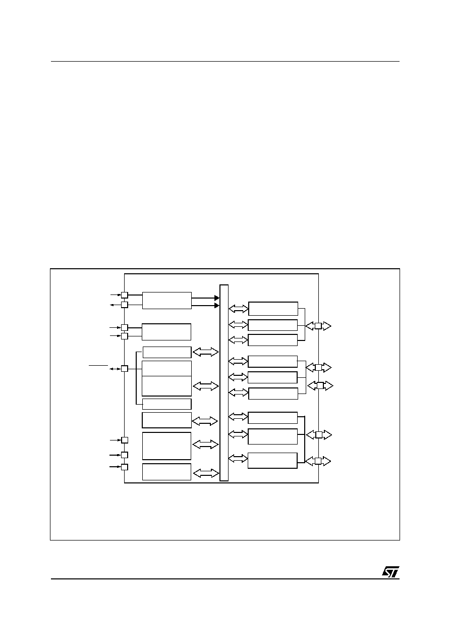
1 INTRODUCTION
The ST7263B Microcontrollers form a sub-family
of the ST7 MCUs dedicated to USB applications.
The devices are based on an industry-standard 8-
bit core and feature an enhanced instruction set.
They operate at a 24 MHz or 12 MHz oscillator fre-
quency. Under software control, the ST7263B
MCUs may be placed in either Wait or Halt modes,
thus reducing power consumption. The enhanced
instruction set and addressing modes afford real
programming potential. In addition to standard 8-
bit data management, the ST7263B MCUs feature
true bit manipulation, 8x8 unsigned multiplication
and indirect addressing modes. The devices in-
clude an ST7 Core, up to 32Kbytes of program
memory, up to 1024 bytes of RAM, 27 I/O lines
and the following on-chip peripherals:
≠ USB low speed interface with 3 endpoints with
programmable in/out configuration using the
DMA architecture with embedded 3.3V voltage
regulator and transceivers (no external compo-
nents are needed).
≠ 8-bit Analog-to-Digital converter (ADC) with 12
multiplexed analog inputs
≠ Industry standard asynchronous SCI serial inter-
face
≠ Watchdog
≠ 16-bit Timer featuring an External clock input, 2
Input Captures, 2 Output Compares with Pulse
Generator capabilities
≠ Fast I≤C Multi Master interface
≠ Low voltage reset (LVD) ensuring proper power-
on or power-off of the device
The ST72F63B devices are Flash versions. They
support programming in IAP mode (In-application
programming) via the on-chip USB interface.
Figure 1. General Block Diagram
8-BIT CORE
ALU
ADD
R
ES
S A
ND DAT
A
BUS
OSCIN
OSCOUT
RESET
PORT B
16-BIT TIMER
PORT A
PORT C
PB[7:0]
(8 bits)
PC[2:0]
(3 bits)
OSCILLATOR
INTERNAL
CLOCK
CONTROL
RAM
(1024 Bytes)
PA[7:0]
(8 bits)
V
SS
V
DD
POWER
SUPPLY
SCI
PROGRAM
(32K Bytes)
I≤C
MEMORY
ADC
1)
(UART)
USB SIE
OSC/3
LVD
WATCHDOG
V
SSA
V
DDA
V
PP
/TEST
USB DMA
USBDP
USBDM
USBVCC
OSC/4 or OSC/2
for USB
2)
PORT D
PD[7:0]
(8 bits)
1)
ADC channels:
2)
12 or 24 MHz OSCIN frequency required to generate 6 MHz USB clock.
None on 24-pin devices
8 on 34 and 32-pin devices (Port B)
12 on 48-pin devices (Port B and Port D[3:0])
ST7263B
5/140
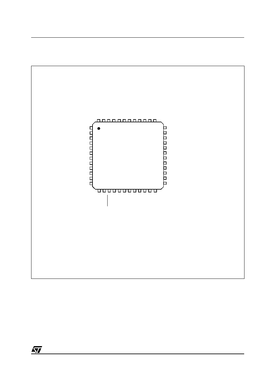
2 PIN DESCRIPTION
Figure 2. 48-Pin TQFP Package Pinout
NC
NC
NC
NC
NC
NC
AIN
7
/IT
8
/PB7
(1
0mA
)
AIN6/IT7/PB6
(1
0mA
)
TDO
/
PC1
RDI/PC0
RES
E
T
NC
48 47 46 45 44 43 42 41 40 39 38 37
36
35
34
33
32
31
30
29
28
27
26
25
13 14 15 16 17 18 19 20 21 22 23
1
2
3
4
5
6
7
8
9
10
11
12
V
DDA
V
DD
OSCOUT
OSCIN
VSS
USBOE/PC2
NC
NC
V
SSA
USBDP
USBDM
USBV
CC
PA7/OCMP2/IT4
PB0
(10mA)
/AIN0
PB1
(10mA)
/AIN1
PB2
(10mA)
/AIN2
PB3
(10mA)
/AIN3
PB4
(10mA)
/AIN4/IT5
PB5
(10mA)
/AIN5/IT6
V
PP
/TEST
PA3/EXTCLK
PA4/ICAP1/IT1
PA5/ICAP2/IT2
PA6/OCMP1/IT3
PD5
PD4
PD3/AIN11
PD2/AIN10
PD1/AIN9
PD0/AIN8
PA2
(2
5mA
)
/
S
CL
/I
CC
C
L
K
NC
PA0/MCO
PA1
(2
5mA
)
/SD
A
/ICCDATA
PD7
PD6
24