
1/9
January 2003
s
UP TO 450mA LOAD CURRENTS
s
200kHz HIGH-FREQUENCY
CURRENT-MODE PWM
s
85% TO 96% EFFICIENCIES
s
33
µ
H OR 100
µ
H PRE-SELECTED
INDUCTOR VALUE, NO COMPONENT
DESIGN REQUIRED
s
0.8mA QUIESCENT CURRENT
s
0.3µA SHUTDOWN SUPPLY CURRENT
s
ADJUSTABLE OUTPUT VOLTAGE
s
OVERCURRENT, SOFT-START AND
UNDERVOLTAGE LOCKOUT PROTECTION
s
CYCLE-BY-CYCLE CURRENT LIMITING
s
PACKAGE AVAILABLE: DIP-8 AND SO-8
DESCRIPTION
The ST730A is a 5V output CMOS, step-down
switching regulator. The ST730A accepts inputs
between 5.2V and 11V and delivers 450mA.
Typical efficiencies are 85% to 96%.
Quiescent supply current is 0.8mA and only 0.3
µ
A
in shutdown mode. The output does not exhibit
frequency over this specified range. Pulse-width
modulation (PWM) current-mode control provides
precise output regulation and excellent transient
responses.
Output
voltage
accuracy
is
guaranteed to be ±5% over line, load, and
temperature varations.
Fixed-frequency
switching
and
absence
of
subharmonic ruipple allows easy filtering of output
ripple and noise, as well as the use of small
external components. This regulators require only
a
single
inductor
value
to
work
in
most
applications, so no inductor design is necessary.
Typical applications are: Cellular phones & radios,
portable Instruments, Portable Communications
Equipments and Computer Peripherals.
ST730A
5V STEP-DOWN,
CURRENT-MODE PWM DC-DC CONVERTERS
SCHEMATIC DIAGRAM
DIP-8
SO-8
ST730A
2/9
ABSOLUTE MAXIMUM RATINGS
Absolute Maximum Ratings are those values beyond which damage to the device may occur. Functional operation under these condition is
not implied.
THERMAL DATA
(*) This value depends from thermal design of PCB on which the device is mounted.
ORDERING CODES
Symbol
Parameter≤
Value
Unit
V
CC
DC Input Voltage
-0.3 to 12
V
V
LX
Switch Pin Voltage
-0.3 to (V
CC
+ 0.3)
V
V
SHDN
Shutdown Voltage (SHDN)
-0.3 to (V
CC
+ 0.3)
V
V
S
,V
C
Soft Start (SS) and Compensation Capacitor (CC) Pins Voltage
-0.3 to (V
CC
+ 0.3)
V
I
LX
Switching Peak Current
2
A
I
REF
Reference Current
2.5
mA
P
TOT
Continuous Power Dissipation at T
A
=70∞C (DIP-8)
(SO-8)
550
344
mW
mW
T
stg
Storage Temperature Range
-40 to +150
∞C
T
op
Operating Junction Temperature Range (C series)
(B series)
0 to +70
-40 to +85
∞C
∞C
Symbol
Parameter
SO-8
DIP-8
Unit
R
thj-amb
Thermal Resistance Junction-ambient (*)
160
100
∞C/W
TYPE
DIP8
SO-8
SO-8 (T&R)
ST730AB
ST730ABN
ST730ABD
ST730ABD-TR
ST730AC
ST730ACN
ST730ACD
ST730ACD-TR
ST730A
3/9
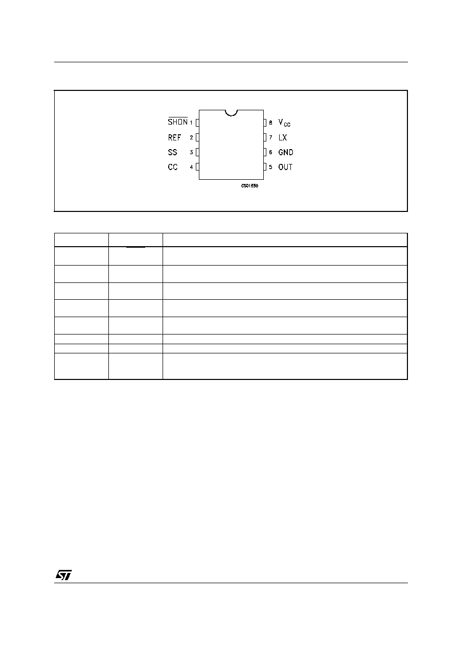
CONNECTION DIAGRAM (top view)
PIN DESCRIPTION
Pin N∞
Symbol
Name and Function
1
SHDN
Shutdown control (active low): If connected to GND the IC is in shutdown.
Connect to V
CC
for normal operation (ON MODE)
2
REF
Reference Output Voltage: (1.25V): Bypass to GND with a capacitor that does not
exceed 47nF
3
SS
Soft Start: a capacitor between SS and GND provides soft-start and short-circuit
protections.
4
CC
Compensation Capacitor Input: externally compensates the outer (voltage)
feedback loop. Connect to OUT with 330pF capacitor
5
OUT
Output Voltage Sense Input: provides regulation of feedback sensing. Connect to
5V output.
6
GND
Ground
7
LX
Switch Output. Drain of internal P-Channel Power MOSFET
8
V
CC
Supply Voltage Input. Bypass to GND with 1
µ
F ceramic capacitance and large
value electrolytic capacitor in parallel. The 1
µ
F capacitor must be as close as
possible to the GND and V
CC
pins
ST730A
4/9
ELECTRICAL CHARACTERISTICS (V
CC
=5V, I
O
= 0mA, T
A
= T
MIN
to T
MAX
, unless otherwise specified.)
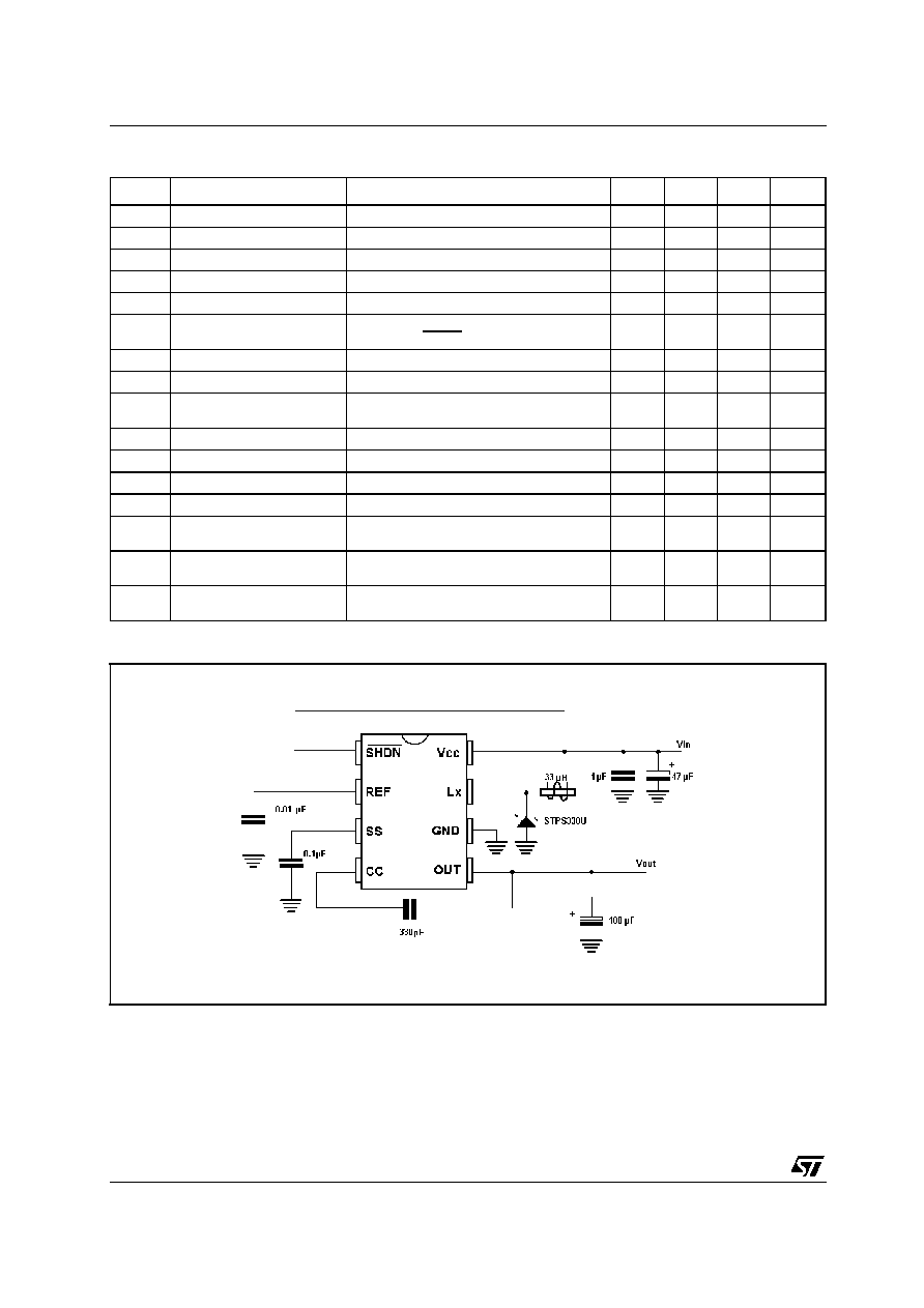
TYPICAL APPLICATION CIRCUIT
Symbol
Parameter
Test Conditions
Min.
Typ.
Max.
Unit
V
CC
Input Voltage
4
11
V
V
O
Output Voltage
V
CC
= 6 to 11V
I
O
=0 to 450mA
4.75
5
5.25
V
V
O
Line Regulation
V
CC
= 5.2 to 11V
0.15
%/V
V
O
Load Regulatio
I
O
= 0 to 450mA
0.005
%/mA
Power Efficency
I
O
=300mA
92
%
I
SUPPLY
Supply Current
ON Mode
OFF Mode, SHDN=0
0.8
0.3
2.5
100
mA
µ
A
V
IH
SHDN Input High Threshold
2
V
V
IL
SHDN Input Low Threshold
0.25
V
I
SHDN
Shutdown Input Leakage
Current
1
µ
A
V
LOCK
Under Voltage Lockout
V
CC
Falling
2.7
3
V
R
DS(on)
LX On Resistance
I
LX
=500mA
0.5
I
LX
LX Leakage Current
V
CC
= 12V
V
LX
= 0V
1
µ
A
V
REF
Reference Voltage
T
A
= 25∞C
1.17
1.24
1.31
V
V
REF
Temperature Reference
Drift
50
ppm/∞C
f
OSC
Switching Frequency
B series
C series
180
160
200
220
280
KHz
R
C
Compensation Pin
Impedance
7500
ST730A
5/9
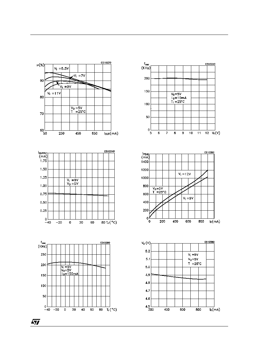
TYPICAL PERFORMANCE CHARACTERISTICS (unless otherwise specified T
j
= 25∞C
Figure 1 : Efficency vs Output Current
Figure 2 : Supply Current vs Temperature
Figure 3 : Oscillator Frequency vs Temperature
Figure 4 : Oscillator Frequency vs Input Voltage
Figure 5 : Peak Inductor Current vs Output
Current
Figure 6 : Output Voltage vs Output Current