 | –≠–ª–µ–∫—Ç—Ä–æ–Ω–Ω—ã–π –∫–æ–º–ø–æ–Ω–µ–Ω—Ç: ST735C | –°–∫–∞—á–∞—Ç—å:  PDF PDF  ZIP ZIP |
1/9
August 2002
s
CONVERTS +4.0V TO + 6.2V INPUT TO -5V
OUTPUT
s
1W GUARANTEED OUTPUT POWER
s
75% TYPICAL EFFICIENCY
s
0.8mA QUIESCENT CURRENT
s
10µA SHUTDOWN MODE
s
160KHZ FIXED FREQUENCY OSCILLATOR
s
CURRENT MODE PWM CONVERTER
s
LOW NOISE AND JITTER
s
SOFT START
s
SIMPLE APPLICATION CIRCUIT
s
UNDERVOLTAGE LOCKOUT
DESCRIPTION
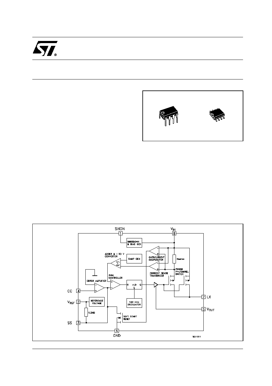
The ST735 is a Bi-CMOS, inverting switch mode
DC-DC regulator with internal Power MOSFET's
that generates a fixed -5V output voltage from a
4V to 6.2V input voltage; is guaranteed an output
current of 200mA for inputs greater than 4.5V. The
quiescent current for this device is typically of
0.8mA and, in shutdown mode it is reduced to
10µA.
These power-conserving features, along with high
efficiency and applications circuits, that lend itself
to minaturization, make the ST735 excellent in a
broad range of on-card, HDD and portable
equipment
applications. The ST735 employ a
high
performance
current
mode
pulse
with
modulation (PWM) control scheme to provide tight
output
voltage regulation and low
noise. The
fixed frequency oscillator is factory trimmed to
160KHz, allowing for easy noise filtering. The
regulator in production is tested to guarantee an
output accuracy within ±5% over all specified
conditions.
ST735
-5V INVERTING, NEGATIVE OUTPUT
CURRENT-MODE PWM REGULATOR
SCHEMATIC DIAGRAM
DIP-8
SO-8
ST735
2/9
ABSOLUTE MAXIMUM RATINGS
Absolute Maximum Ratings are those values beyond which damage to the device may occur. Functional operation under these condition is
not implied.
THERMAL DATA
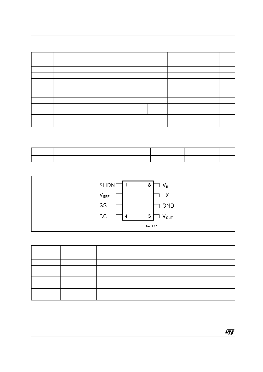
CONNECTION DIAGRAM (top view)
PIN DESCRIPTION
Symbol
Parameter
Value
Unit
V
IN
DC Input Voltage (V
IN
to GND)
-0.3 to +7
V
SHDN
Shutdown Voltage (SHDN to GND)
-0.3 to V
+
+0.3
V
V
LX
Switch Voltage (Lx to V
IN
)
-12.5 to +0.3
V
V
FB
Feedback Voltage (V
OUT
to GND)
-11 to +0.3
V
V
OUT
Output Voltage (V
OUT
to GND)
-11 to +0.3
V
Other Input Voltage (SS, CC to GND)
-0.3 to V
+
+0.3
V
I
LX
Peack Switch Current
2
A
P
tot
Power Dissipation at T
j
= 70∞C
DIP-8
725
mW
SO-8
470
T
stg
Storage Temperature Range
-55 to +150
∞C
T
op
Operating Junction Temperature Range
-40 to +125
∞C
Symbol
Parameter
DIP-8
SO-8
Unit
R
thj-case
Thermal Resistance Junction-case
2
8
∞C/W
Pin N∞
Symbol
Name and Function
1
SHDN
SHUT-DOWN Control (V
CC
=ON GND=Shutdown
2
V
REF
Reference Output Voltage
3
SS
Soft Start
4
CC
Compensation Input
5
V
OUT
Negative Output Voltage
6
GND
Ground
7
LX
Switch Output
8
V
IN
Positive Supply - Voltage Input
ST735
3/9
ORDERING CODES
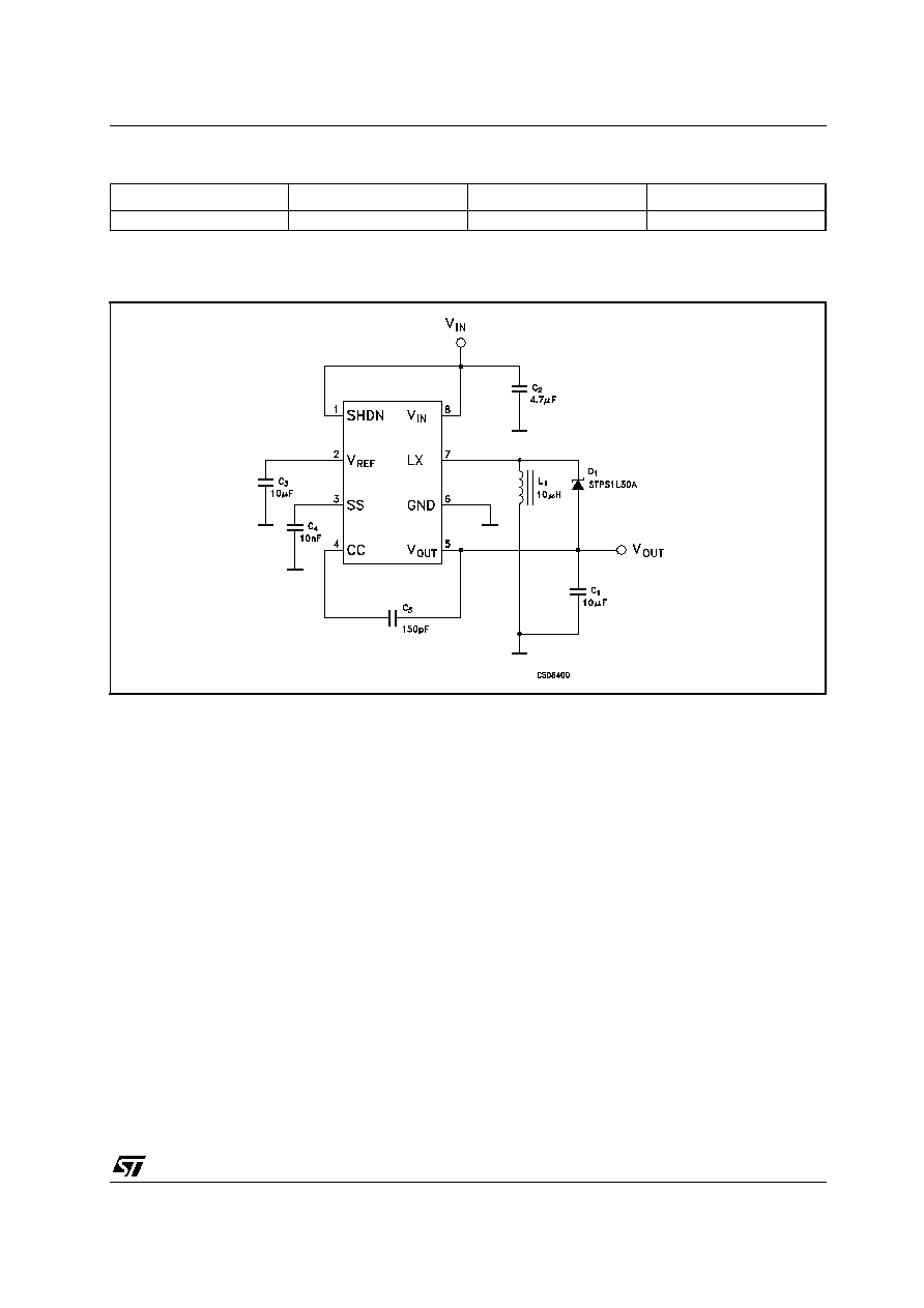
TYPICAL APPLICATION CIRCUIT
NOTE:
1) All capacitors are X7R ceramic
2) C
5
can be omitted if are used higher values for the input and output capacitors C
2
=47
µ
F, C
1
=100pF.
TYPE
DIP-8
SO-8
SO-8 (T&R)
ST735
ST735CN
ST735CD
ST735CD-TR
ST735
4/9
ELECTRICAL CHARACTERISTICS (Refer to test circuit, V
IN
=5V, C
IN
= 4.7
µ
F, C
OUT
= 10
µ
F, L = 10
µ
H,
T
amb
= -40 to 125∞C, unless otherwise specified. Typical value are referred at T
amb
= 25∞C)
Note1 : Tested at I
VREF
= 0mA
Symbol
Parameter
Test Conditions
Min.
Typ.
Max.
Unit
V
IN
Input Voltage
4
6.2
V
V
OUT
Output Voltage
V
IN
= 4.5V to 6.2V I
OUT
= 0 to 200mA
T
amb
= -40 to 125
∞C
-5.25
-5
-4.75
V
V
IN
= 4.0V to 6.2V I
OUT
= 0 to 175mA
T
amb
= -40 to 125
∞C
-5.25
-5
-4.75
V
I
OUT
Output Current
V
IN
= 4.5V to 6.2V T
amb
= 0 to 125
∞
C
200
275
mA
V
IN
= 4.5V to 6.2V I
OUT
= 0 to 175mA
T
amb
= -40 to 125
∞C
175
mA
V
IN
= 4.0V
V
OUT
= -5V
175
mA
I
SUPPLY
Supply Current
Includes Switch Current
0.8
1.6
mA
I
STANDBY
Standby Current
V
SHDN
= 0V
1
10
µ
A
I
SC
Short Circuit Current
1.5
A
V
LO
Undervoltage Lock-out
3.5
4
V
V
OUT
Line Regulation
V
IN
= 4.0V to 6.2V
0.1
%/V
V
OUT
Load Regulation
I
OUT
= 0 to 200mA
0.003
%/mA
V
REF
Reference Voltage
T
amb
= 25
∞
C (Note 1)
1.247
V
V
REF
Reference Drift
T
amb
= -40 to 125
∞
C
50
ppm/∞C
R
DSON
LX ON Voltage
0.5
I
LEAK
LX Leakage Current
V
DS
= 10V
1
µ
A
I
SH
Shutdown Pin Current
1
µ
A
V
IL
Shutdown Input Low
Threshold
0.25
V
V
IH
Shutdown Input High
Threshold
2
V
f
OSC
Maximum Oscillator
Frequency
160
KHz
Efficency
I
OUT
= 100mA
72
%
R
CC
Compensation Pin
Impedance on CC Pin
7.5
K
ST735
5/9
TYPICAL CHARACTERISTICS (Referred to typical application circuit, T
amb
=25∞C unless otherwise specified)
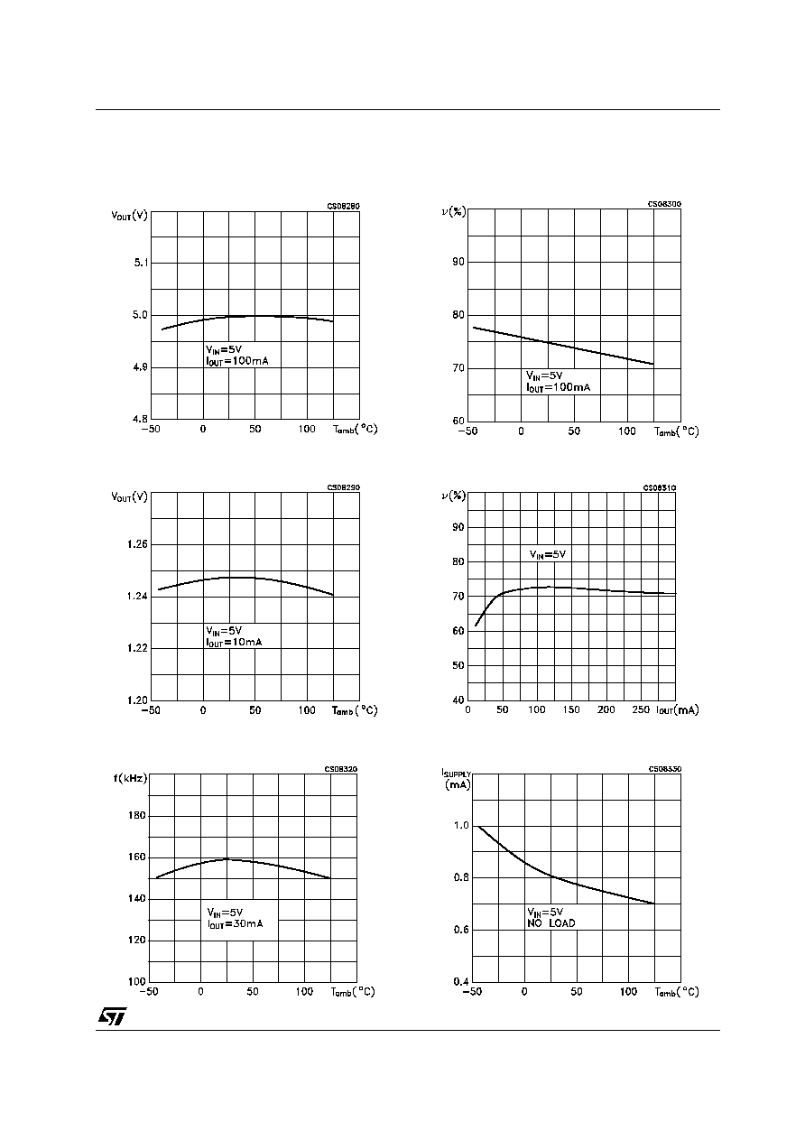
Figure 1 : Output Voltage vs Temperature
Figure 2 : Reference Voltage vs Temperature
Figure 3 : Oscillator Frequency vs Temperature
Figure 4 : Efficency vs Temperature
Figure 5 : Efficency vs Ouput Current
Figure 6 : Supply Current vs Temperature