1/13
December 2002
s
MEETS AND EXCEEDS THE
REQUIREMENTS OF EIA/TIA-232-E AND
ITUV.28 STANDARD
s
SINGLE CHIP WITH EASY INTERFACE
BETWEEN UART AND SERIAL PORT
CONNECTOR OF IBM PC/AT
TM
AND
COMPATIBLES
s
DESIGNED TO SUPPORT DATA RATES UP
TO 120 Kbps
DESCRIPTION
The ST75285 contains six drivers and ten
receivers.
The
pinout
matches
the
DB9S
connector design in order to decrease the part
count, reduce the board space required and allow
easy interconnection of the UART and serial port
connector of IBM PC/AT
TM
and compatibles. The
bipolar circuits and processing of the ST75285
provides a rugged low-cost solution for this
function at the expense of quiescent power and
external passive components relative to the
ST75C185.
The ST75285 complies with the requirements of
the EIA/TIA 232-E and ITU (formally CCITT) v.28
standards.
These
standards
are
for
data
interchange
between
a
host
computer
and
peripheral at signalling rates up to 20k-bits/s. The
switching speeds of the ST75285 are fast enough
to support rates up to 120K-bits/s with lower
capacitive loads (shorter cables). Interoperability
at the higher signalling rates cannot be assured
unless the designer has design control of the
cable and the interface circuits at the both ends.
For interoperability at signalling rates to 120
K-bits/s, use of EIA/ITA-423-B (ITU v.10) and EIA/
ITA-422-B
(ITU
v.11)
standards
are
recommended.
It
allows
space
saving
in
applications where two ST75185 are needed.
ORDERING CODES
Type
Temperature
Range
Package
Comments
ST75285CTR
0 to 70 �C
TSSOP38 (Tape & Reel)
2500 parts per reel
ST75285
MULTIPLE RS-232 DRIVERS AND RECEIVERS
TSSOP
ST75285
2/13
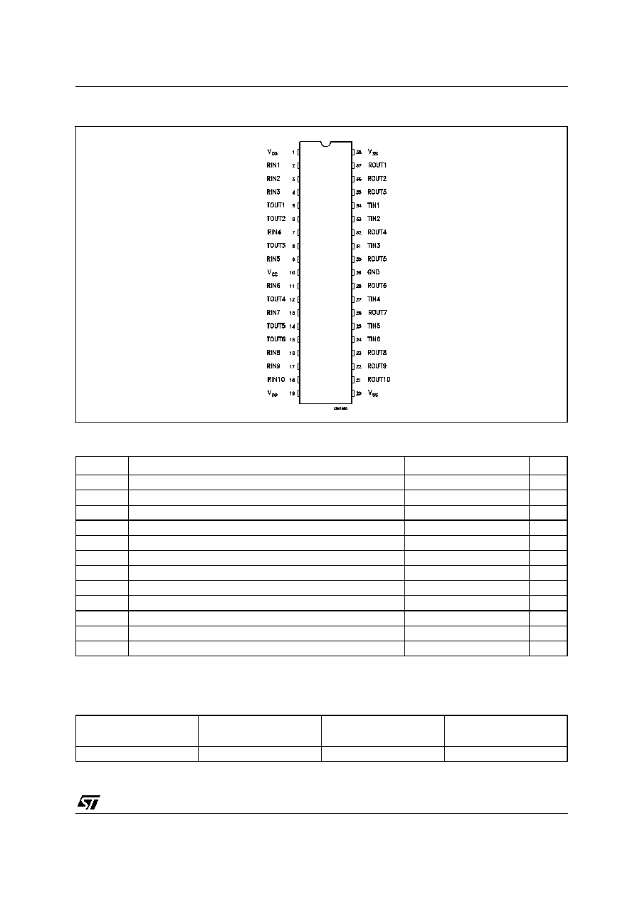
PIN DESCRIPTION
PlN N�
SYMBOL
NAME AND FUNCTION
1
V
DD
Supply Voltage (+12V)
2
RIN1
First Receiver Input
3
RIN2
Second Receiver Input
4
RIN3
Third Receiver Input
5
TOUT1
First Driver Output
6
TOUT2
Second Driver Output
7
RIN4
Fourth Receiver Input
8
TOUT3
Third Driver Output
9
RIN5
Fifth Receiver Input
10
V
CC
Supply Voltage (-12V)
11
RIN6
Sixth Receiver Input
12
TOUT4
Fourth Driver Output
13
RIN7
Seventh Receiver Input
14
TOUT5
Fifth Driver Output
15
TOUT6
Sixth Driver Output
16
RIN8
Eighth Receiver Input
17
RIN9
Nineth Receiver Input
18
RIN10
Tenth Receiver Input
19
V
DD
Supply Voltage (-12V)
20
V
SS
Supply Voltage (+5V)
21
ROUT10
Tenth Receiver Ouput
22
ROUT9
Nineth Receiver Ouput
23
ROUT8
Eighth Receiver Ouput
24
TIN6
Sixth Driver Input
25
TIN5
Fifth Driver Input
26
ROUT7
Seventh Receiver Ouput
27
TIN4
Fourth Driver Input
28
ROUT6
Sixth Receiver Output
29
GND
Ground
30
ROUT5
Fifth Receiver Output
31
TIN3
Third Driver Input
32
ROUT4
Fourth Receiver Output
33
TIN2
Second Driver Input
34
TIN1
First Driver Input
35
ROUT3
Third Receiver Ouput
36
ROUT2
Second Receiver Ouput
37
ROUT1
First Receiver Ouput
38
V
SS
Supply Voltage (+5V)
ST75285
3/13
PIN CONNECTION IEC LOGIC SYMBOL AND LOGIC DIAGRAM
ABSOLUTE MAXIMUM RATINGS OVER OPERATING FREE-AIR TEMPERATURE RANGE
Absolute Maximum Ratings are those values beyond which damage to the device may occur. Functional operation under these condition is
not implied.
NOTE 1: All voltage are with respect to the network ground terminal.
DISSIPATION RATING TABLE
(*) This is the reverse of the traditional junction-case thermal resistance R
tJ-C
Symbol
Parameter
Value
Unit
V
DD
Supply Voltage (Note 1)
-0.3 to 15
V
V
SS
Supply Voltage (Note 1)
0.3 to -15
V
V
CC
Supply Voltage (Note 1)
-0.3 to 10
V
V
I
Input Voltage Range (DRIVER)
-15 to 7
V
V
I
Input Voltage Range (RECEIVER)
-30 to 30
V
V
O
Output Voltage Range (DRIVER)
-15 to 15
V
I
O
Receiver Low Level Output Current
20
mA
P
D
Continuous Total Power Dissipation
See dissipation Rating Table
T
A
Operating Free-Air Tempereature Range
0 to 70
�C
T
stg
Storage Temperature Range
-65 to + 150
�C
ESD
Human Body Model
>2
kV
T
L
Lead Temperature 1.6mm from case for 10 sec
260
�C
Package
Power Rating
at T
A
25�C
Derating Factor
above T
A
=
25�C (*)
Power Rating
at T
A
85�C
TSSOP (T)
1277 mW
10.2 mW/�C
644 mW
ST75285
4/13
RECOMMENDED OPERATING CONDITIONS
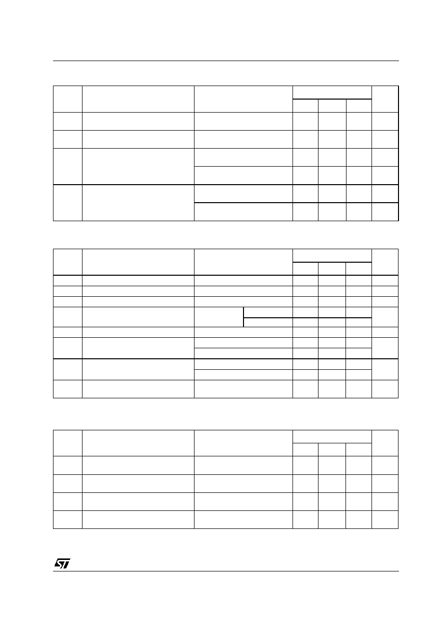
SUPPLY CURRENTS
DRIVER ELECTRICAL CHARACTERISTICS OVER OPERATING FREE-AIR TEMPERATURE
RANGE (V
DD
= 9V, V
SS
= -9V, V
CC
= 5V, unless otherwise specified)
NOTE 3: The algebraic convention, where the more positive (less negative) limits designated as maximum, is used in this datasheet for logic
levels only (e.g. if - 10V is a maximum, the typical value is a more negative voltage).
NOTE 4: Output short circuit conditions must maintain the total power dissipation below absolute maximum ratings.
NOTE 5: Test conditions are those specified by EIA-232-E and as listed above.
Symbol
Parameter
Min
Max
Unit
V
DD
Supply Voltage
7.5
15
V
V
SS
Supply Voltage
-7.5
-15
V
V
CC
Supply Voltage
4.5
5.5
V
V
I
Driver Input Voltage
0
V
CC
V
I
OH
High Level Output Current
DRIVER
-6
mA
RECEIVER
-0.5
I
OL
Low Level Output Current
DRIVER
6
mA
RECEIVER
16
T
A
Operating Free-Air Tempereature
0
70
�C
Symbol
Parameter
Test Conditions
Value
Unit
V
DD
V
SS
Min.
Typ.
Max.
I
DD
Supply Current from V
DD
9
-9
No load.
All inputs at
1.9V
22
mA
12
-12
28
15
-15
32
9
-9
No load.
All inputs at
0.8V
9
mA
12
-12
11
15
-15
12
I
SS
Supply Current from V
SS
9
-9
No load.
All inputs at
1.9V
-22
mA
12
-12
-28
15
-15
-32
9
-9
No load.
All inputs at
0.8V
-6.4
mA
12
-12
-6.4
15
-15
-6.4
I
CC
Supply Current from V
CC
No load. All inputs at 5V
V
CC
= 5V
60
mA
Symbol
Parameter
Test Conditions
Value
Unit
Min.
Typ.
Max.
V
OH
High Level Output Voltage
V
IL
= 0.8 V R
L
= 3K
(See Figure 1)
6
7.5
V
V
OL
Low Level Output Voltage
(Note 3)
V
IH
= 1.9 V R
L
= 3K
(See Figure 1)
-7.5
-6
V
I
IH
High Level Input Current
V
I
= 5 V (See Figure 2)
10
�
A
I
IL
Low Level Input Current
V
I
= 0 V (See Figure 2)
-
1.6
mA
I
OS(H)
High Level Short Circuit
Output Current (Note 4)
V
IL
= 0.8 V
V
O
= 0 V (See Figure 1)
-4.5
-
12
-
19.5
mA
I
OS(L)
Low Level Short Circuit
Output Current
V
IH
= 2 V
V
O
= 0 V (See Figure 1)
4.5
12
19.5
mA
R
O
Output Resistance
V
DD
= V
SS
= V
CC
= 0 V
V
O
= -2 to 2 V (Note 5)
300
ST75285
5/13
DRIVER SWITCHING CHARACTERISTICS (V
DD
= 12V, V
SS
= -12V, V
CC
= 5V, T
A
= 25 �C)
NOTE 6: Measured between -3V and 3V points of output waveform (EIA-232-E conditions), all unused inputs are tied.
RECEIVER ELECTRICAL CHARACTERISTICS OVER OPERATING CONDITIONS
All typical values are at TA = 25�C, VCC = 5V, VDD = 9V and VSS=-9V
RECEIVER SWITCHING CHARACTERISTICS (V
DD
= 12V, V
SS
= -12V, V
CC
= 5V T
A
= 25�C)
Symbol
Parameter
Test Conditions
Value
Unit
Min.
Typ.
Max.
t
PLH
Propagation Delay Time, Low to High
Level Output
R
L
= 3 to 7 K
C
L
= 15 pF
(See Figure 3, 4)
200
400
ns
t
PHL
Propagation Delay Time, High to Low
Level Output
R
L
= 3 to 7 K
C
L
= 15 pF
(See Figure 3, 4)
50
100
ns
t
TLH
Transition Time Low to High Level
Output
R
L
= 3 to 7 K
C
L
= 15 pF
(See Figure 3, 4)
60
100
ns
R
L
= 3 to 7 K
C
L
= 2500 pF
(Note 6, See Figure 3, 4)
1.7
2.5
�
s
t
THL
Transition Time High to Low Level
Output
R
L
= 3 to 7 K
C
L
= 15 pF
(See Figure 3, 4)
50
100
ns
R
L
= 3 to 7 K
C
L
= 2500 pF
(Note 6, See Figure 3, 4)
1.5
2.5
�
s
Symbol
Parameter
Test Conditions
Value
Unit
Min.
Typ.
Max.
V
T+
Positive Going Threshold Voltage
(See Figure 6)
2.2
2.4
V
V
T-
Negative Going Threshold Voltage
T
A
= 25 �C (See Figure 6)
0.75
0.97
V
V
hys
Input Hysteresis (V
T+
- V
T-
)
0.5
V
V
OH
High Level Output Voltage
I
OH
= -0.5mA
V
IH
= 0.75 V
2.6
4
5
V
Inputs Open
2.6
V
OL
Low Level Output Voltage
V
I
= 3 V
I
OL
= 10 mA
0.2
0.45
V
I
IH
High Level Input Current
V
I
= 25 V (See Figure 6)
3.6
8.3
mA
V
I
= 3 V
(See Figure 6)
0.43
I
IL
Low Level Input Current
V
I
= -25 V (See Figure 6)
-3.6
-8.3
mA
V
I
= -3 V
(See Figure 6)
-0.43
I
OS
Short-Circuit Output Current
V
I
= 0 V
V
O
= 0 V
(See Figure 5)
-3.4
-12
mA
Symbol
Parameter
Test Conditions
Value
Unit
Min.
Typ.
Max.
t
PLH
Propagation Delay Time Low to High
Level Output
R
L
= 5 K
C
L
= 50 pF
(See Figure 6)
200
500
ns
t
PHL
Propagation Delay Time High to Low
Level Output
R
L
= 5 K
C
L
= 50 pF
(See Figure 6)
60
120
ns
t
TLH
Transition Time Low to High Level
Output
R
L
= 5 K
C
L
= 50 pF
(See Figure 6)
200
525
ns
t
THL
Transition Time High to Low Level
Output
R
L
= 5 K
C
L
= 50 pF
(See Figure 6)
20
60
ns