ST7537HS1
HOME AUTOMATION MODEM
June 1995
18
1
2
3
4
5
6
7
8
9
10
11
19
20
21
22
23
24
25
26
27
28
12
13
14
15
16
17
DV
CC
RSTO
RxD
TxD
CD
Rx/Tx
WD
Rx
F
O
RAI
AV
DD
V
CM
AV
SS
DE
M
I
IF
O
T
EST
3
TE
S
T
4
XT
A
L
1
XT
A
L
2
MC
L
K
DV
DD
DV
SS
PAFB
ATO
PABC
PABC
TEST1
TEST2
TxIFI
75
37
H
-
01
.
E
P
S
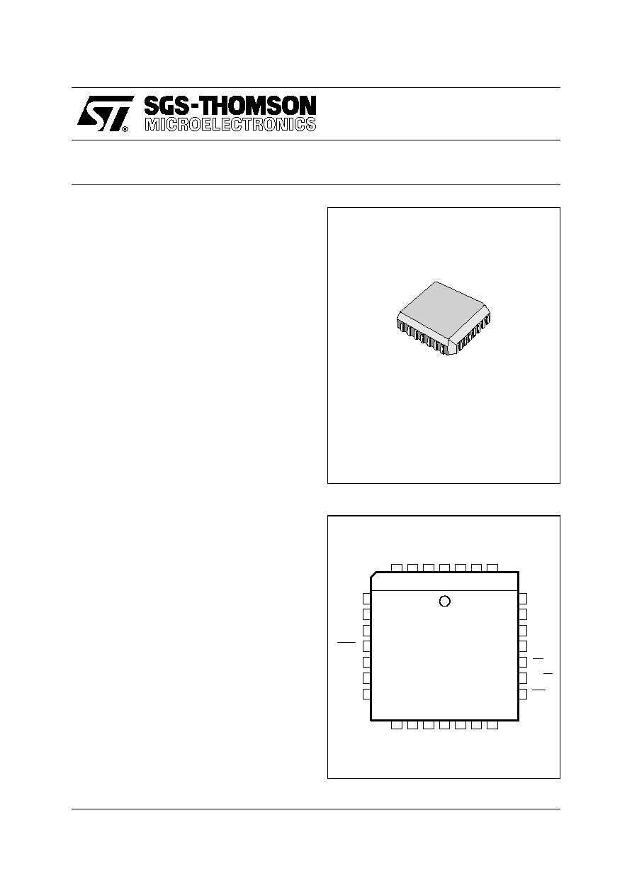
PIN CONNECTIONS
PLCC28
(Plastic Chip Carrier)
ORDER CODE : ST7537HS1
.
HALF DUPLEX ASYNCHRONOUS 2400bps
FSK MODEM
.
Tx CARRIER FREQUENCY SYNTHESIZED
FROM EXTERNAL CRYSTAL
.
LOW DISTORTION Tx SIGNAL
.
Rx SENSITIVITY BETTER THAN 1mV
RMS
.
CARRIER DETECTION
.
WATCH-DOG INPUT
.
RESET AND MASTER CLOCK OUTPUTS
FOR MICROCONTROLLER
.
POWER AMPLIFIER BIAS CURRENT CON-
TROL (HIGH IMPEDANCE IN Rx MODE)
.
SIMPLE AND ECONOMICAL APPLICATION
SCHEMATICS
.
COMPATIBLE WITH CENELEC EN 50065-1
AND FCC SPECIFICATION
.
CARRIER DETECT CLAMPING ON RxD
PROGRAMMABLE (ALLOWING DEMODULA-
TION ON VERY LOW RECEIVE LEVEL,
1mV
RMS
TYPICALLY)
DESCRIPTION
The ST7537HS1 is a half duplex asynchronous
FSK MODEM designed for home automation com-
munication on the domestic electric mains which
complies with the EN 50065-1 CENELEC stand-
ard.
It mainly operates from a 10V power supply and a
5V power supply for the microcontroller digital in-
terface.
It is interfaced to the power line by an external
driver, and a transformer (see Application Sche-
matic Diagram). Its data transmission rate is
2400 bps and its carrier frequency is 132.45kHz.
1/9
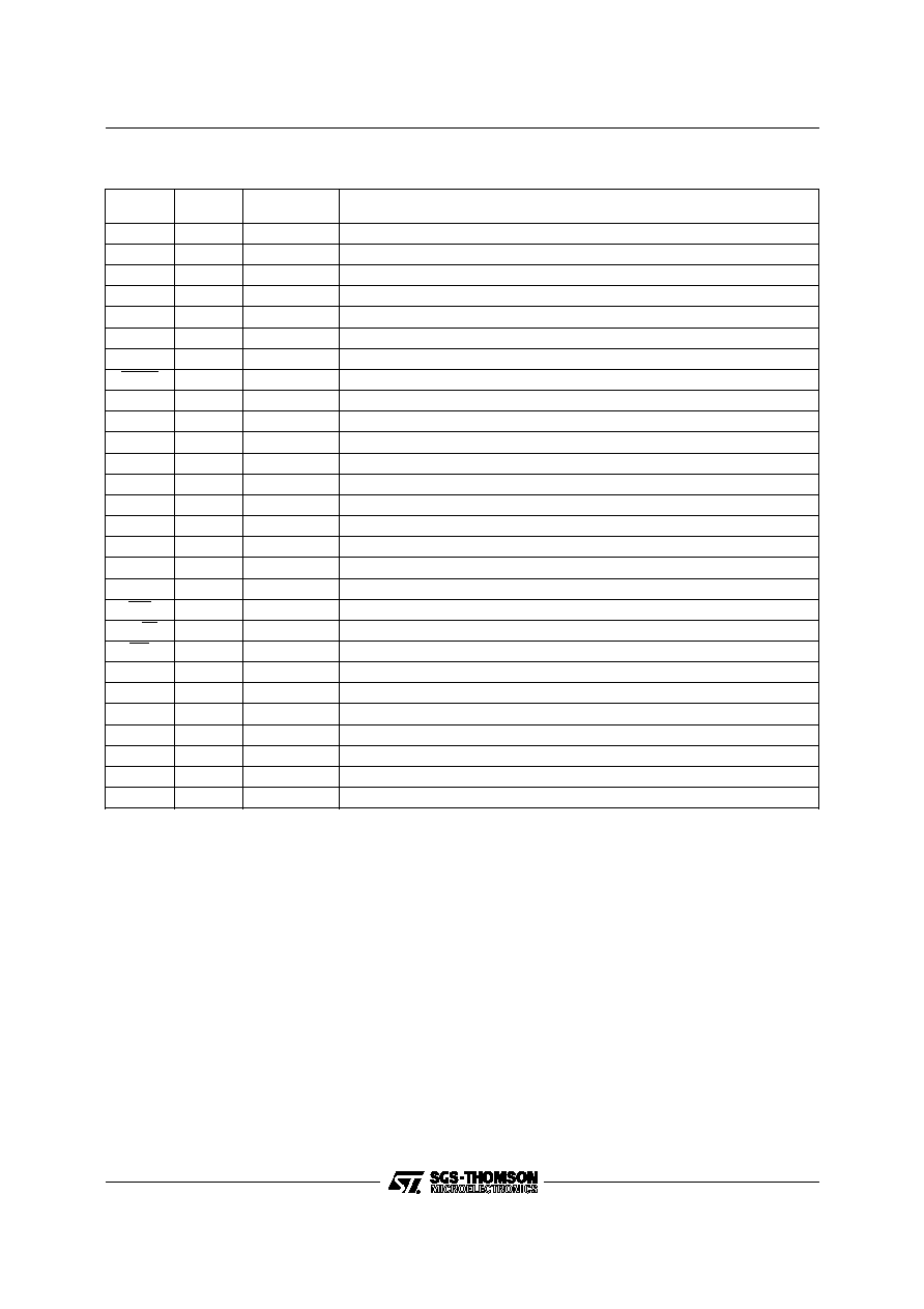
PIN DESCRIPTION
Pin
Name
Pin
Number
Pin
Type
Description
V
CM
1
Analog
Common Mode Voltage
AV
DD
2
Supply
Analog Power Supply : 10V
�
5 %
RAI
3
Analog
Receive Analog Input
RxFO
4
Analog
Receive Filter Output
TxIFI
5
Analog
Transmit and Intermediate Frequency Filters Test Input (mode TEST3)
PAFB
6
Analog
Power Amplifier Feed-back Input
ATO
7
Analog
Analog Transmit Output
PABC
8
Digital (10V)
Power Amplifier Bias Current Control Complementary Output
PABC
9
Digital (10V)
Power Amplifier Bias Current Control Output
TEST1
10
Digital
Tx to Rx Automatic Mode Switching Control Input
TEST2
11
Digital
Automatic Mode Switching Time and Watch-dog Time Reduction Control Input
TEST3
12
Digital
TxIFI Selection Input
TEST4
13
Digital
Undelayed Reset Input
DV
DD
14
Supply
Digital Power Supply : 10V
�
5%
DV
SS
15
Supply
Digital Ground : 0V
XTAL1
16
Digital (10V)
Crystal Oscillator Input
XTAL2
17
Digital (10V)
Crystal Oscillator Output
MCLK
18
Digital
Master Clock Output
WD
19
Digital
Watch-dog Input
Rx/Tx
20
Digital
Rx or Tx Mode Selection Input
CD
21
Digital
Carrier Detect Output
TxD
22
Digital
Transmit Data Input
RxD
23
Digital
Receive Data Output
RSTO
24
Digital
Reset Output
DV
CC
25
Supply
Digital Buffers Supply Voltage : 5V
�
5 %
IFO
26
Analog
Intermediate Frequency Filter Output
DEMI
27
Analog
Demodulator Input
AV
SS
28
Supply
Analog Ground : 0V
75
37
H
-
01
.
T
B
L
ST7537HS1
2/9
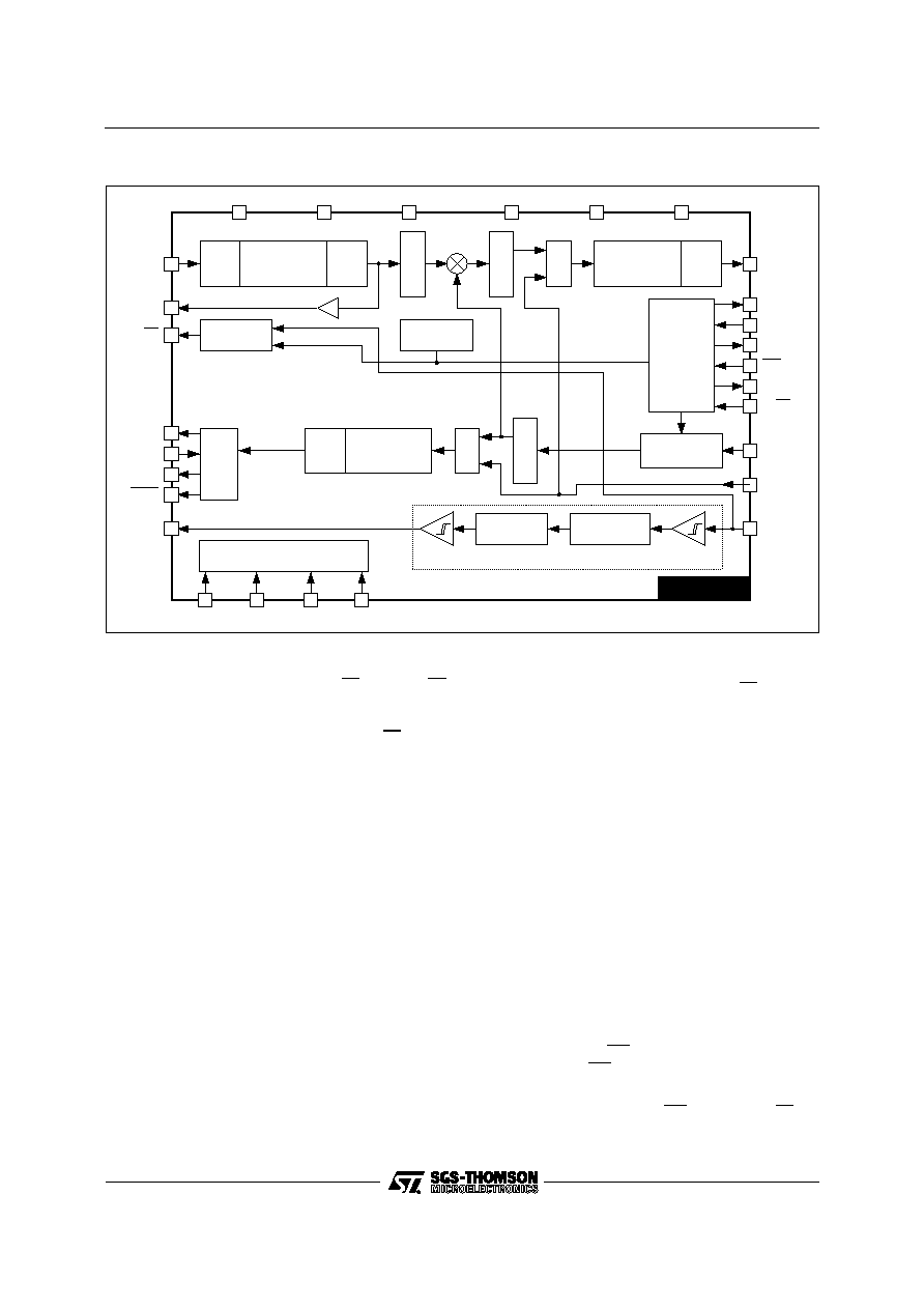
REFERENCE
VOLTAGE
CARRIER
DETECTION
A.A.
FILTER
Rx BAND-PASS
S.C. FILTER
SMT.
FILTER
A.A. FILTER
MU
X
SMT.
FILTER
Tx BAND-PASS
S.C. FILTER
OUTPUT
AMPLIFIER
CORRELATOR
POST-DEMO
S.C. FILTER
FSK DEMODULATOR
27
5
13
12
11
10
7
6
9
8
FSK
MODULATOR
17
16
18
19
24
20
CONTROL LOGIC
TIME BASE
RESET LOGIC
22
23
MU
X
A.A. FILTER
SMT.
FILTER
I.F. BAND-PASS
S.C. FILTER
3
20dB GAIN
26
4
21
2
14
28
15
1
25
RAI
RxFO
CD
ATO
PAFB
PABC
PABC
RxD
IFO
XTAL1
XTAL2
MCLK
WD
RSTO
Rx/Tx
TxD
DEMI
TxIFI
AV
DD
DV
DD
AV
SS
DV
SS
V
CM
DV
CC
TEST LOGIC
TEST1
TEST2
TEST3
TEST4
ST7537HS1
75
37
H
-
02
.
E
P
S
BLOCK DIAGRAM
TRANSMIT SECTION
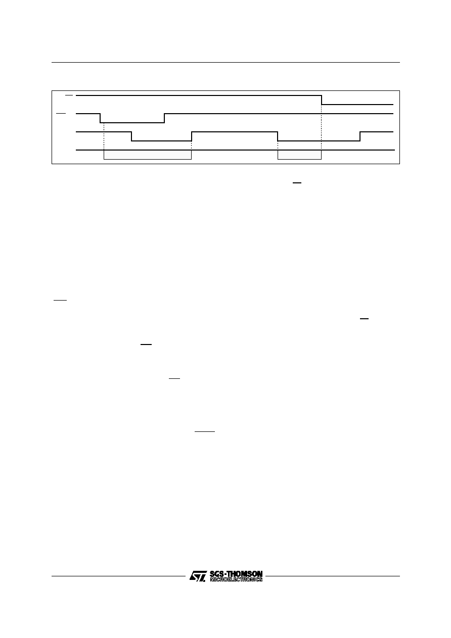
The transmit mode is set when Rx/Tx = 0, if Rx/Tx
is held at 0 longer than 1 second, then the device
switches automatically in the Rx mode. A new
activation of the Tx mode requires Rx/Tx to be
returned to 1 for a minimum 2 microsecond period
before being set to 0.
The Transmit Data (TxD) enter asynchronously the
FSK modulator with a nominal intra-message data
rate of 2400 bps.
The basic transmit frequencies are :
- f(TxD=0) = 133.05kHz
- f(TxD=1) = 131.85kHz
These frequencies are synthesized from a
11.0592MHz crystal oscillator; their precision is the
same as the crystal one's (100ppm).
The modulated signal coming out of the FSK modu-
lator is filtered by a switched-capacitor band-pass
filter (Tx band-pass) in order to limit the output
spectrum and to reduce the level of harmonic com-
ponents.
The final stage of the Tx path consists of an opera-
tional amplifier which needs a feed-back signal
(PAFB) from the power amplifier as shown on
Application Schematic Diagram.
In Tx mode the Receive Data (RxD) signal is set to 1.
RECEIVE SECTION
The receive section is active when Rx/Tx = 1.
The Rx signal is applied on RAI and filtered by a
band-pass switched capacitor filter (Rx band-pass)
centered on the carrier frequency and whose band-
width is around 12kHz.
The Rx filter output is amplified by a 20dB gain
stage which provides symetrical limitations for
large voltage. The resulting signal is down-con-
verted by a mixer which receives a local oscillator
synthesized by the FSK modulator block. Finally an
intermediate frequency band-pass filter (IF band-
pass) whose central frequency is 5.4kHz improves
the signal to noise ratio before entering the FSK
demodulator.
The coupling of the intermediate frequency filter
output (IFO) to the FSK demodulator input (DEMI)
is made by an external capacitor C5 (100nF
�
10%,
10V) which cancels the Rx path offset voltage.
The RxD output delivers the demodulated signal if
the carrier detect (CD) signal is low and is set to
high level when CD = 1.
The RxD output can delivers the demodulated
signal whatever the level of CD (0 or 1) if Rx/Tx = 1
and TxD = 0 (see Figure 1).
ST7537HS1
3/9
ADDITIONAL DIGITAL AND ANALOG FUNC-
TIONS
Time base
A time base section delivers all the internal clocks
from a crystal oscillator (11.0592MHz). The crystal
is connected between XTAL1 and XTAL2 pins and
needs two external capacitors C3 and C4 (22pF
�
10%, 10V) for proper operation.
Reset and watch-dog
The reset output (RSTO) is driven high when the
supply voltage is lower than Vrh (typically 7.6V) with
an hysteresis Vrh-Vrl (typically 300mV) or when no
negative transition occurs on the watch-dog input
(WD) for more than 1.5 second (see the timing
chart on Figure 2). When a reset occurs RSTO is
held high for at least 50ms.
Signal detection
The Carrier Detect output (CD) is driven low when
the input signal amplitude on RAI is greater than
V
CD
for at least T
CD
(typically 6ms see the timing
chart on Figure 3). When the input signal desap-
pears or becomes lower than V
CD
, CD is held low
for at least Tcd before returning to a high level. V
CD
is the carrier detection threshold voltage which is
set internally to detect 5mV
RMS
typically.
External power amplifier bias control
Two dedicated digital output (PABC and PABC)
delivering a signal between 0V and 10V are driven
low respectively high, when the circuit is set in the
receive mode (Rx/Tx=1) or when the transmit mode
time out (1 second) is exceeded; in the same time
the output ATO is put in a high impedance state.
TESTING FEATURES
- An additionnal amplifier allows the observation of
the Rx band-pass filter output on pin RxFO.
- A direct input to the Tx band-pass filter and to the
IF filter (TxIFI) is selected when TEST3 = 1.
- The 1 second normal duration of the Tx to Rx
mode automatic switching is reduced to 488
�
s
and the 1.5 second watch-dog time out is reduced
to 46.3
�
s when TEST2 = 1.
- When TEST1 = 1 the Tx to Rx mode automatic
switching is desactivated and the functional mode
of the circuit is fully controlled by Rx/Tx.
- TEST4 is a reset input which allows an undelayed
control of RSTO and of the internal state of the
circuit.
POWER SUPPLIES WIRING PRECAUTIONS
The ST7537HS1 has two positive power supply
terminals (AV
DD
,DV
DD
) and two ground terminals
(AV
SS
,DV
SS
) in order to separate internal analog
and digital supplies. The analog and digital termi-
nals of each supply pair must be connected to-
gether externally for proper operation.
The V
DD
must be protected against short-circuit for
proper operation.
Rx/Tx
CD
TxD
RxD
DATA
DATA
75
37
H
-
03
.
E
P
S
Figure 1 : Data Timing Chart
ST7537HS1
4/9
ABSOLUTE MAXIMUM RATINGS
Symbol
Parameter
Value
Unit
AV
DD
/DV
DD
Supply Voltage (1)
- 0.3, + 12
V
V
I
Digital Input Voltage
DV
SS
- 0.3, DV
DD
+ 0.3
V
V
O
Digital Output Voltage (microcontroller interface)
DV
SS
- 0.3, DV
CC
+ 0.3
V
V
O
Digital Output Voltage (PABC and PABC)
DV
SS
- 0.3, DV
DD
+ 0.3
V
I
O
Digital Output Current
- 5, + 5
mA
V
I
Analog Input Voltage
AV
SS
- 0.3, AV
DD
+ 0.3
V
V
O
Analog Output Voltage
AV
SS
- 0.3, AV
DD
+ 0.3
V
I
O
Analog Output Current
- 5, + 5
mA
P
D
Power Dissipation
500
mW
T
oper
Operating Temperature
0, + 70
o
C
T
stg
Storage Temperature
- 55, + 150
o
C
75
37
H
-
02
.
T
B
L
Notes :
1.
The voltages are referenced to AV
SS
and DV
SS
.
2.
Absolute maximum ratings are values beyond which damage to device may occur. Functional operation under
these conditions is not implied.
GENERAL ELECTRICAL CHARACTERISTICS
(A/DV
DD
= 10V, A/DV
SS
= 0V, DV
CC
= 5V and 0
o
C
T
amb
70
o
C, unless otherwise specificied)
Symbol
Parameter
Test Conditions
Min.
Typ.
Max.
Unit
AV
DD
DV
DD
Supply Voltage
9.5
10
10.5
V
AI
DD
+
DI
DD
Supply Current
30
mA
DV
CC
Digital Output Supply Voltage
4.75
5.25
V
DI
CC
Digital Output Supply Current
1.5
mA
V
IH
High Level Input Voltage
Digital Inputs
4.2
V
V
IL
Low Level Input Voltage
Digital Inputs
0.8
V
V
OH
High Level Output Voltage
I
OH
= -100
�
A
�
Digital Outputs
�
Digital Outputs PABC and PABC
4.9
9.8
V
V
V
OL
Low Level Output Voltage
I
OL
= 100
�
A
�
Digital Outputs
�
Digital Outputs PABC and PABC
0.1
0.2
V
V
DC
Duty Cycle
MCLK Output, C
L
= 15pF
40
60
%
75
37
H
-
0
3
.
T
B
L
TRANSMITTER ELECTRICAL CHARACTERISTICS
(A/DV
DD
= 10V, A/DV
SS
= 0V, DV
CC
= 5V and 0
o
C
T
amb
70
o
C, unless otherwise specificied)
Symbol
Parameter
Test Conditions
Min.
Typ.
Max.
Unit
VTAC
Max Carrier Output AC Voltage
R
L
= 5.6k
R
L
(AV
SS
) = 5.6k
R(ATO, PAFB) = 1k
0.8
1.0
1.3
V
RMS
HD2
Second Harmonic Distortion
- 50
dB
HD3
Third Harmonic Distortion
- 60
dB
FD
FSK Peak-to-peak Deviation
1200
Hz
75
37
H
-
0
4
.
T
B
L
ST7537HS1
5/9