 | –≠–ª–µ–∫—Ç—Ä–æ–Ω–Ω—ã–π –∫–æ–º–ø–æ–Ω–µ–Ω—Ç: ST7538 | –°–∫–∞—á–∞—Ç—å:  PDF PDF  ZIP ZIP |
1/30
ST7538
September 2003
s
HALF DUPLEX FREQUENCY SHIFT KEYING
(FSK) TRANSCEIVER
s
INTEGRATED POWER LINE DRIVER WITH
PROGRAMMABLE VOLTAGE AND CURRENT
CONTROL
s
PROGRAMMABLE INTERFACE:
≠ SYNCHRONOUS
≠ ASYNCHRONOUS
s
SINGLE SUPPLY VOLTAGE (FROM 7.5 UP TO 12.5V)
s
VERY LOW POWER CONSUMPTION (Iq=5 mA)
s
INTEGRATED 5V VOLTAGE REGULATOR
(UP TO 100mA) WITH SHORT CIRCUIT
PROTECTION
s
8 PROGRAMMABLE TRANSMISSION
FREQUENCIES
s
PROGRAMMABLE BAUD RATE UP TO 4800BPS
s
RECEIVING SENSITIVITY 1 mVRMS
s
SUITABLE TO APPLICATION IN ACCORDANCE
WITH EN 50065 CENELEC SPECIFICATIONS
s
CARRIER OR PREAMBLE DETECTION
s
BAND IN USE DETECTION
s
PROGRAMMABLE REGISTER WITH
SECURITY CHECKSUM
s
MAINS ZERO CROSSING DETECTION AND
SYNCHRONIZATION
s
WATCHDOG TIMER
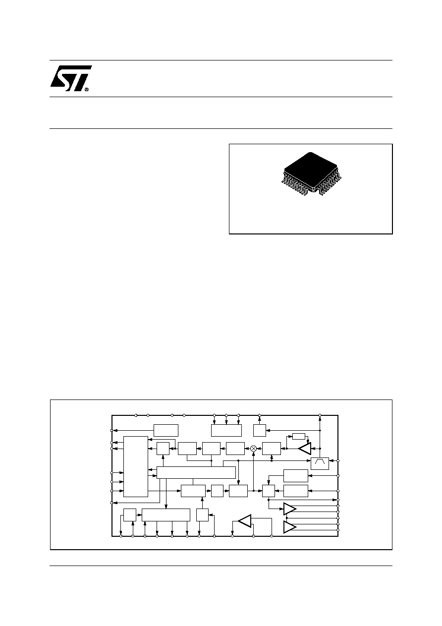
DESCRIPTION
The ST7538 is a Half Duplex synchronous/asyn-
chronous FSK Modem designed for power line
communication network applications. It operates
from a single supply voltage and integrates a line
driver and a 5V linear regulator. The device oper-
ation is controlled by means of an internal register,
programmable through the synchronous serial in-
terface. Additional functions as watchdog, clock
output, output voltage and current control, pream-
ble detection, time-out, band in use are included.
Realized in Multipower BCDV technology that al-
lows to integrate DMOS, Bipolar and CMOS struc-
tures in the same chip.
TQFP44 Slug Down
ORDERING NUMBER: ST7538P
POWER LINE FSK TRANSCEIVER
BLOCK DIAGRAM
SERIAL
INTERFACE
CARRIER
DETECTION
PLL
CD/PD
RxD
CLR/T
REG/DATA
RxTx
TxD
REGOK
PG
Vdc
PAVcc
ATOP2
ATOP1
ATO
Vsense
CL
RAI
RxFo
TEST2 TEST3
TEST1
AVdd
DVdd
AVss
DVss
BU
XOut
WD
TOUT
RSTO
MCLK
ZCin
ZCout
C_OUT
CMINUS
CPLUS
XIn
DIGITAL
FILTER
FSK
DEMOD
IF
FILTER
TX
FILTER
FILTER
+
-
FILTER
BU
DAC
ZC
OSC
AGC
AMPL
TEST
ALC
OP-AMP
PLI
VREG
CURRENT
CONTROL
VOLTAGE
CONTROL
FSK
MODULATOR
TIME BASE
CONTROL
REGISTER
D03IN1407
ST7538
2/30
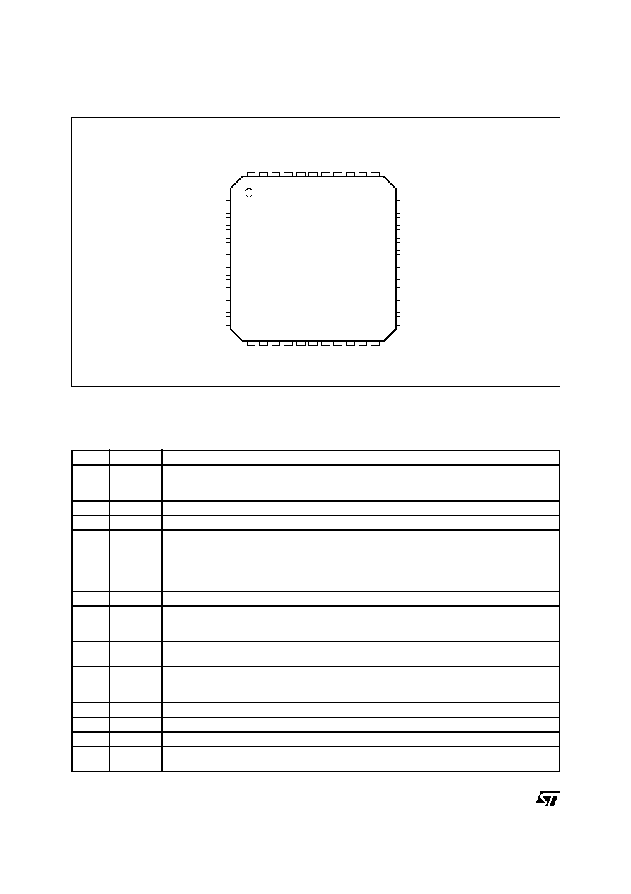
PIN CONNECTION (Top view)
PIN DESCRIPTION
N∞
Name
Type
Description
1
CD_PD
Digital/Output
Carrier or Preamble Detect Output.
"1" No Carrier or Preamble Detected
"0" Carrier or Preamble Detected
2
DVss
Supply
Digital Ground
3
RxD
Digital/Output
RX Data Output.
4
RxTx
Digital/Input
with internal pull-up
Rx or Tx mode selection input.
"1" - RX Session
"0" - TX Session
5
TxD
Digital/Input
with internal pull-down
TX Data Input.
6
GND
Supply
Substrate Ground (same function as PIN 41)
7
TOUT
Digital/Output
TX Time Out Event Detection
"1" - Time Out Event Occurred
"0" - No Time-out Event Occurred
8
CLR/T
Digital/Output
Synchronous Mains Access Clock or
Control Register Access Clock
9
BU
Digital/Output
Band in use Output.
"1" Signal within the Programmed Band
"0" No Signal within the Programmed Band
10
DVdd
Supply
Digital Supply Voltage
11
MCLK
Digital/Output
Master Clock Output
12
RSTO
Digital/Output
Power On or Watchdog Reset Output
13
TEST 3
Digital/Input
with internal pull-down
Test Input. Must be connected to DVss during Normal Operation
1
2
3
5
6
4
7
8
9
10
17
11
18
19
20
21
22
44
43
42
41
39
40
38
37
36
35
34
28
27
26
24
23
25
33
32
31
29
30
CD_PD
DVSS
RXD
RxTx
TXD
GND
TOUT
CLR/T
BU
DVDD
MCLK
RSTO
TEST3
WD
ZCOUT
ZCIN
N.C.
DVSS
ATOP1
PAVSS
ATOP2
PAVCC
N.C.
TEST1
REG_OK
C_MINUS
C_PLUS
N.C.
C_OUT
GND
PG
REG_DATA
N.C.
CL
ATO
SGND
XOUT
XIN
AVDD
VSENSE
TEST2
RXFO
RAI
VDC
D01IN1312
12
13
14
15
16
3/30
ST7538
14
WD
Digital/Input
with internal pull-up
Watchdog input. The Internal Watchdog Counter is cleared on the
falling edges.
15
ZCOUT
Digital/Output
Zero Crossing Detection Output
16
ZCIN
1
Analog/Input
Zero Crossing AC Input.
17
NC
Floating
Must be connected to DVss.
18
DVss
Supply
Digital Ground
19
ATOP1
Power/Output
Power Line Driver Output
20
PAVss
Supply
Power Analog Ground
21
ATOP2
Power/Output
Power Line Driver Output
22
PAV
CC
Supply
Power Supply Voltage
23
CL
2
Analog/Input
Current Limiting Feedback.
A resistor between CL and AVss sets the PLI Current Limiting Value
24
ATO
Analog/Output
Small Signal Analog Transmit Output
25
SGND
Supply
Analog Signal Ground
26
XOUT
Analog I/O
Crystal Output- External Clock Input
27
XIN
Analog Input
Crystal Oscillator Input
28
AVdd
Supply
Analog Power supply.
29
Vsense
3
Analog/Input
Output Voltage Sensing input for the voltage control loop
30
TEST2
Analog/Input
Test Input must be connected SGND
31
RxFO
Analog/Output
Receiving Filter Output
32
RAI
Analog/Input
Receiving Analog Input
33
VDC
Power
5V Voltage Regulator Output
34
NC
floating
Must Be connected to DVss.
35
TEST1
Digital/Input
with internal pull-down
Test input. Must Be connected to DVss.
36
REGOK
Digital/Output
Security checksum logic output
"1" - Stored data Corrupted
"0" - Stored data OK
37
C_MINUS
4
Analog/Input
Op-amp Inverting Input.
38
C_PLUS
5
Analog/Input
Op-amp Not Inverting Input.
39
NC
floating
Must Be connected to DVss
40
C_OUT
Analog/Output
Op-amp Output
41
GND
Supply
Substrate Ground (same function as PIN 6)
42
PG
Digital/Output
Power Good logic Output
"1" - VDC is above 4.5V
"0" - VDC is below 4.25V
43
REG_DATA
Digital/Input
with internal pull-down
Mains or Control Register Access Selector
"1" - Control Register Access
"0" - Mains Access
44
NC
floating
Must be connected to DVss.
<1>
If not used this pin must be connected to VDC
<2>
Cannot be left floating
<3>
Cannot be left floating
<4>
If not used this pin must be connected to VDC
<5>
If not used this pin must be tied low (SGND or PAVss or DVss)
PIN DESCRIPTION (continued)
N∞
Name
Type
Description
ST7538
4/30
ABSOLUTE MAXIMUM RATINGS
THERMAL DATA
(*) Mounted on Multilayer PCB with a dissipating surface on the bottom side of the PCB
(**) It's the same condition of the point above, without any heatsinking surface on the board.
Symbol
Parameter
Value
Unit
PAV
CC
Power Supply Voltage
-0.3 to +14
V
AV
dd
Analog Supply Voltage
-0.3 to +5.5
V
DV
dd
Digital Supply Voltage
-0.3 to +5.5
V
AV
ss
/DV
ss
Voltage between AV
ss
and DV
ss
-0.3 to +0.3
V
V
I
Digital input Voltage
DV
ss
- 0.3 to DV
dd
+0.3
V
V
O
Digital output Voltage
DV
ss
- 0.3 to DV
dd
+0.3
V
I
O
Digital Output Current
-2 to +2
mA
V
sense
Voltage Range at Vsense Input
AV
ss
- 0.3 to AV
dd
+0.3
V
RAI
Voltage Range at RAI Input
-AV
dd
- 0.3 to AV
dd
+0.3
V
ATO
Output Current at ATO Output
-2 to +2
mA
ATO
Voltage range at ATO Output
AV
ss
- 0.3 to AV
dd
+0.3
V
ATOP1,2
Voltage range at Powered ATO Output
AV
ss
- 0.3 to +PAV
cc
+0.3
V
ATOP
Powered ATO Output Current
400
mARms
T
amb
Operating ambient Temperature
-40 to +85
∞C
T
stg
Storage Temperature
-50 to 150
∞C
ATOP1 Pin
Maximum Withstanding Voltage Range
Test Condition: CDF-AEC-Q100-002- "Human Body Model"
Acceptance Criteria: "Normal Performance"
±1500
V
ATOP2 Pin
±1000
V
Other pins
±2000
V
Symbol
Parameter
TQFP44
with slug
Unit
R
th-j-amb1
Maximum Thermal Resistance Junction-Ambient Steady State(*)
35
∞
C/W
R
th-j-amb2
Maximum Thermal Resistance Junction-Ambient Steady State(**)
50
∞
C/W
5/30
ST7538
ELECTRICAL CHARACTERISTCS
(AVcc = DVcc = +5V, PAVcc =+9 V, PAVss, SGND = DVss = 0V,-40∞C
Tamb
85∞C, unless otherwise specified)
Symbol
Parameter
Test Condition
Min.
Typ.
Max.
Unit
AV
CC
,
DV
CC
Supply Voltages
4.75
5
5.25
V
PAV
CC
- DV
CC
PAV
CC
and DV
CC
Relation
during Power-Up Sequence
DV
CC
< 4.75V
0.1
1.2
V
PAV
CC
- AV
CC
PAV
CC
and DV
CC
Relation
during Power-Up Sequence
AV
CC
< 4.75V
0.1
1.2
V
PAV
cc
Power Supply Voltage
7.5
12.5
V
Max allowed slope during
Power-Up
10
V/ms
AI
CC
+ DI
CC
Input Supply Current
Transmission & Receiving mode
5
7
mA
I PAV
CC
Powered Analog Supply
Current
TX mode (no load)
30
50
mArms
RX mode
500
1000
µ
A
Maximum total current
370
mArms
Digital I/O
V
IH
High Logic Level Input Voltage
2
V
V
IL
Low Logic Level input Voltage
0.8
V
V
OH
High Logic Level Output Voltage I
OH
= -2mA
3.5
V
V
OL
Low Logic Level Output Voltage I
OL
= 2mA
0.4
V
Oscillator
V
IHX
XIN High Level Input Voltage
External Clock
3
V
V
ILX
XIN Low Level Input Voltage
External Clock
2
V
DC
XTAL Clock Duty Cycle
External Clock
40
60
%
Xtal
Crystal Oscillator frequency
16
MHz
Tclock
Oscillator Period (1/Xtal)
62.5
ns
Xtal
ESR
External Oscillator Esr
Resistance
40
Ohm
Xtal
CL
External Oscillator Stabilization
Capacitance
16
pF
Transmitter
IATOP
Output Transmitting Current in
programmable current limiting
Vsense connected though a
100pF cap to GND; Rcl=1.85k
;
R
LOAD
=1
(as in fig. 13)
250
310
370
mArms
V
ATO
Max Carrier Output AC Voltage R
CL
= 1.85k
Vsense=0V
1.75
2.3
3.5
V
PP
V
ATODC
Output DC Voltage on ATO
1.7
2.1
2.5
V
HD2
ATO
Second Harmonic Distortion on
ATO
V
ATO
= 2V
PP
; Fc=86KHz
-55
-42
dB
HD3
ATO
Third Harmonic Distortion on
ATO
V
ATO
= 2V
PP
; Fc=86KHz
-52
-49
dB
V
ATOP(AC)
Max Carrier Output AC Voltage
for each ATOP1 and ATOP2
pins
R
CL
= 1.85k
Vsense=0V
3.5
4.6
6
V
pp
V
ATOP(DC)
Output DC Voltage on ATOP1
and ATOP2 pins
3.5
4.2
5
V
PAVcc
VAT OP A C
(
)
2
------------------------------------
7.5V
+