 | ÐлекÑÑоннÑй компоненÑ: ST7540 | СкаÑаÑÑ:  PDF PDF  ZIP ZIP |
Äîêóìåíòàöèÿ è îïèñàíèÿ www.docs.chipfind.ru
September 2006
Rev 2
1/44
44
ST7540
FSK power line transceiver
General features
Half-duplex frequency shift keying (FSK)
transceiver
Integrated power line driver with programmable
voltage and current control
Programmable mains access:
Synchronous
Asynchronous
Single supply voltage (from 7.5V up to 13.5V)
Very low power consumption (I
q
= 5mA)
Integrates 5V voltage regulator (up to 50mA)
with short circuit protection
Integrated 3.3V voltage regulator (up to 50mA)
with short circuit protection
3.3V or 5V digital supply
8 Programmable transmission frequencies
Programmable baud rate up to 4800BPS
Receiving sensitivity up to 250
µV
RMS
Suitable for applications in accordance with EN
50065 Cenelec specification
Carrier or preamble detection
Band in use detection
Programmable control register
Watchdog timer
8 or 16 Bit header recognition
ST7537 and ST7538 compatible
UART/SPI host interface
Description
The ST7540 is a Half Duplex
synchronous/asynchronous FSK Modem
designed for power line communication network
applications. It operates from a single supply
voltage and integrates a line driver and two linear
regulators for 5V and 3.3V. The device operation
is controlled by means of an internal register,
programmable through the synchronous serial
interface. Additional functions as watchdog, clock
output, output voltage and current control,
preamble detection, time-out and band in use are
included. Realized in Multipower BCD5
technology that allows to integrate DMOS, Bipolar
and CMOS structures in the same chip.
HTSSOP28 Exposed Pad
www.st.com
Order codes
Part number
Package
Packaging
ST7540
HTSSOP28 (Exposed Pad)
Tube
ST7540TR
HTSSOP28 (Exposed Pad)
Tape and reel

Contents
ST7540
2/44
Contents
1
Block diagram . . . . . . . . . . . . . . . . . . . . . . . . . . . . . . . . . . . . . . . . . . . . . . 4
2
Pin settings . . . . . . . . . . . . . . . . . . . . . . . . . . . . . . . . . . . . . . . . . . . . . . . . 5
2.1
Pin connection . . . . . . . . . . . . . . . . . . . . . . . . . . . . . . . . . . . . . . . . . . . . . . 5
2.2
Pin description . . . . . . . . . . . . . . . . . . . . . . . . . . . . . . . . . . . . . . . . . . . . . . 5
3
Electrical data . . . . . . . . . . . . . . . . . . . . . . . . . . . . . . . . . . . . . . . . . . . . . . 7
3.1
Maximum ratings . . . . . . . . . . . . . . . . . . . . . . . . . . . . . . . . . . . . . . . . . . . . 7
3.2
Thermal data . . . . . . . . . . . . . . . . . . . . . . . . . . . . . . . . . . . . . . . . . . . . . . . 7
3.3
Recommended operating conditions . . . . . . . . . . . . . . . . . . . . . . . . . . . . . 8
4
Electrical characteristics . . . . . . . . . . . . . . . . . . . . . . . . . . . . . . . . . . . . . 9
5
Crystal resonator and external clock . . . . . . . . . . . . . . . . . . . . . . . . . . 15
6
Functional description . . . . . . . . . . . . . . . . . . . . . . . . . . . . . . . . . . . . . . 16
6.1
Carrier frequencies . . . . . . . . . . . . . . . . . . . . . . . . . . . . . . . . . . . . . . . . . . 16
6.2
Baud rates . . . . . . . . . . . . . . . . . . . . . . . . . . . . . . . . . . . . . . . . . . . . . . . . 16
6.3
Mark and space frequencies . . . . . . . . . . . . . . . . . . . . . . . . . . . . . . . . . . 17
6.4
ST7540 Mains access . . . . . . . . . . . . . . . . . . . . . . . . . . . . . . . . . . . . . . . 18
6.5
Host processor interface . . . . . . . . . . . . . . . . . . . . . . . . . . . . . . . . . . . . . 19
6.5.1
Communication between Host and ST7540 . . . . . . . . . . . . . . . . . . . . . 20
6.5.2
Control register access . . . . . . . . . . . . . . . . . . . . . . . . . . . . . . . . . . . . . 22
6.6
Receiving mode . . . . . . . . . . . . . . . . . . . . . . . . . . . . . . . . . . . . . . . . . . . . 23
6.7
Transmission mode . . . . . . . . . . . . . . . . . . . . . . . . . . . . . . . . . . . . . . . . . 26
6.8
Control register . . . . . . . . . . . . . . . . . . . . . . . . . . . . . . . . . . . . . . . . . . . . . 32

ST7540
Contents
3/44
7
Auxiliary analog and digital functions . . . . . . . . . . . . . . . . . . . . . . . . . 36
7.1
Band in use . . . . . . . . . . . . . . . . . . . . . . . . . . . . . . . . . . . . . . . . . . . . . . . 36
7.2
Time out . . . . . . . . . . . . . . . . . . . . . . . . . . . . . . . . . . . . . . . . . . . . . . . . . . 36
7.3
Reset & watchdog . . . . . . . . . . . . . . . . . . . . . . . . . . . . . . . . . . . . . . . . . . 37
7.4
Output clock . . . . . . . . . . . . . . . . . . . . . . . . . . . . . . . . . . . . . . . . . . . . . . . 37
7.5
Output voltage level freeze . . . . . . . . . . . . . . . . . . . . . . . . . . . . . . . . . . . . 37
7.6
Extended control register . . . . . . . . . . . . . . . . . . . . . . . . . . . . . . . . . . . . . 37
7.7
Under voltage lock out . . . . . . . . . . . . . . . . . . . . . . . . . . . . . . . . . . . . . . . 38
7.8
Thermal shutdown . . . . . . . . . . . . . . . . . . . . . . . . . . . . . . . . . . . . . . . . . . 38
7.9
5V Voltage regulator . . . . . . . . . . . . . . . . . . . . . . . . . . . . . . . . . . . . . . . . . 38
7.10
3.3V Voltage regulator . . . . . . . . . . . . . . . . . . . . . . . . . . . . . . . . . . . . . . . 38
7.11
Power-up procedure . . . . . . . . . . . . . . . . . . . . . . . . . . . . . . . . . . . . . . . . . 38
8
Mechanical data . . . . . . . . . . . . . . . . . . . . . . . . . . . . . . . . . . . . . . . . . . . . 41
9
Revision history . . . . . . . . . . . . . . . . . . . . . . . . . . . . . . . . . . . . . . . . . . . 43

Block diagram
ST7540
4/44
1 Block
diagram
Figure 1.
Block diagram
SERIAL
INTERFACE
CARRIER
DETECTION
PLL
CD/PD
RxD
CLR/T
REG/DATA
RxTx
TxD
Vdc
V
CC
PA_OUT
TX_OUT
Vsense
CL
RX_IN
TEST2
UART/SPI
TEST1
BU/THERM
X1
WD
RSTO
MCLK
X2
DIGITAL
FILTER
FSK
DEMOD
IF
FILTER
TX
FILTER
FILTER
FILTER
BU
DAC
OSC
AGC
AMPL
TEST
ALC
PA
VREG
CURRENT
CONTROL
VOLTAGE
CONTROL
FSK
MODULATOR
TIME BASE
CONTROL
REGISTER
D03IN1407A
PA_IN-
+
-
PA_IN+
V
SS
VREG
V
DD
SV
SS
GND
ST7540
Pin settings
5/44
2 Pin
settings
2.1 Pin
connection
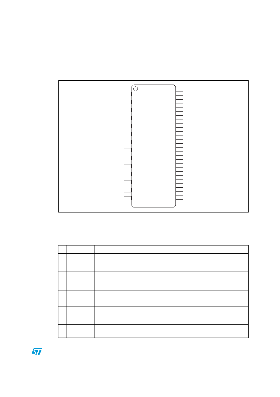
Figure 2.
Pin connection (top view)
2.2 Pin
description
1
2
3
4
5
6
7
8
9
10
11
12
13
14
28
27
26
25
24
23
22
21
20
19
18
17
16
15
CD_PD
REG_DATA
GND
RxD
RxTx
TxD
BU/THERM
CLR/T
V
DD
MCLK
RSTO
UART/SPI
WD
PA_IN-
TEST2
TEST1
VDC
RX_IN
CL
Vsense
X2
X1_OSCIN
SV
SS
TX_OUT
PA_IN+
V
CC
V
SS
PA_OUT
Table 1. Pin description
N°
Name
Type
Description
1
CD_PD
Digital/Output
Carrier, preamble or frame header detect output.
"1" No carrier, preamble or frame header detected
"0" Carrier, preamble or frame header detected
2
REG_DATA
Digital/Input
with internal pull-down
Mains or control register access selector
"1" - Control register access
"0" - Mains access
3
GND
Supply
Digital ground
4
RxD
Digital/Output
RX data output.
5
RxTx
Digital/Input
with internal pull-up
Rx or Tx mode selection input.
"1" - RX Session
"0" - TX Session
6
TxD
Digital/Input
with internal pull-down
TX data input.
Document Outline