ST7554
V.90 USB WORLD MODEM CONTROLLER
January 1999
SUMMARY DATA
TQFP48 (7 x 7 x 1.40mm)
(Full Plastic Quad Flat Pack)
ORDER CODE : ST7554TQF7
GENERAL
.
USB HOT PLUG & PLAY INTERFACE
.
DIRECT INTERFACE TO ST MAFE+DAA
CHIP-SET ST75951/ST952 FOR WORLD-
WIDE DAA DESIGN OR TO STLC7550 FOR
TRADITIONAL DAA DESIGN
.
WINDOWS
Æ
98 AND NT 5.0 SUPPORT
.
TAPI 2.0 COMPLIANT
.
SOFTWARE UPGRADABLE
.
MINIMUM SYSTEM REQUIREMENTS:
.
USB MOTHERBOARD, 166MHz PENTIUM
Æ
PROCESSOR WITH MMX
TM
TECHNOLOGY,
WINDOWS
Æ
98 AND 16MBYTES RAM OR
WINDOWS
Æ
NT 5.0 AND 32MBYTES RAM
DEVICE FEATURES
.
SINGLE 9.216MHz CRYSTAL OSCILLATOR
.
INTEGRATED ANALOG AND DIGITAL 3.3V
REGULATORS
.
DEDICATED PINS FOR RING, OFF-HOOK,
CLID, LOOP CURRENT SENSE
.
0.5
µ
m CMOS PROCESS
.
TQFP48 (7 x 7 mm) PACKAGE
DATA MODEM / FAX / VOICE
.
V.90
.
V.34BIS, V.34, V.32BIS, V.32, V.22BIS, V.22,
V.23, V.21
.
BELL 103 AND BELL 212A
.
V.17, V.27TER, V.29, FAX CLASS 1 SUPPORT
.
V.42, V.42BIS, MNP 2, 3, 4, 5
.
V.80
.
V.8 AND AUTO MODE
.
VOICE / FAX / MODEM DISTINCTION
.
ADPCM VOICE COMPRESSION/DECOM-
PRESSION
.
VOICE DETECTION (SILENCE DETECTION)
OTHER FEATURES
.
VIRTUAL UART (460.8Kbps)
.
AT HAYES COMMAND COMPATIBLE
.
TIME INDEPENDENT ESCAPE SEQUENCE
(TIES) COMMAND
.
CALLER ID
This is advance information on a new product now in development or undergoing evaluation. Details are subject to change without notice.
.
DTMF DETECTION AND GENERATION
.
WAKE UP ON RING
.
WORLD-WIDE PROGRAMMABLE SILICON
DAA SUPPORT FOR ST75951/ST952
MAFE+DAA CHIP-SET
UNIVERSAL SERIAL BUS
.
SPECIFICATION 1.0, 12MBps FULL SPEED
.
ON-CHIP USB TRANSCEIVER WITH DIGITAL PLL
.
COMMUNICATION DEVICE CLASS AND
VENDOR REQUESTS
.
BUS OR SELF POWERED APPLICATION
(PIN-PROGRAMMABLE)
.
ONNOW POWER MANAGEMENT (D0, D2, D3)
.
LOW POWER CONSUMPTION (SUSPEND
MODE D2), WHOLE APPLICATION BELOW
500
µ
A
DESCRIPTION
The ST7554 is a single chip host signal processing
Modem/fax/voice controller that supports data rates
up to 56Kbps. All data pump and protocol functions
are executed on the host PC's processor. This
product has been developed in cooperation with
Smart Link Ltd, who ported "USB-Modio", its host
based Modem and system software into ST system
and hardware platform. The ST7554 directly con-
nects to ST high performance Modem analog front-
end (MAFE) STLC7550 or to the highly integrated
MAFE+DAA chip-set ST75951/ST952. The ST7554
also features an Universal Serial Bus (USB) inter-
face for direct connection to the host PC for maxi-
mum flexibility and real plug & play operation.
1/11
1
2
3
4
5
6
7
8
16
15
14
13
9
10
11
17
18
19
20
21
22
26
25
28
27
30
29
31
32
33
37
39
38
41
40
42
43
44
12
23
24
34
35
36
45
46
47
48
D-
D+
GNDBUS
VREGD
VBUS
VREGA
AGND
PSM
XTALIN
XTALOUT
FLTPLL
RESET
DC
TRxD
DAASEL
RESERVED
DGND
DOUT
DIN
MCLK
FS
HC1
PDOWN
RESERVED
BUZEN
PULSE
DI
SHS
RFC
LED
CD
RESERVED
RESERVED
CLI
D
HO
HSDT
RI
RESERVED
RESERVED
RESERVED
RESERVED
RESERVED
RESERVED
RESERVED
RESERVED
RESERVED
RESERVED
RESERVED
RESERVED
75
54
S
-
0
1.
E
P
S
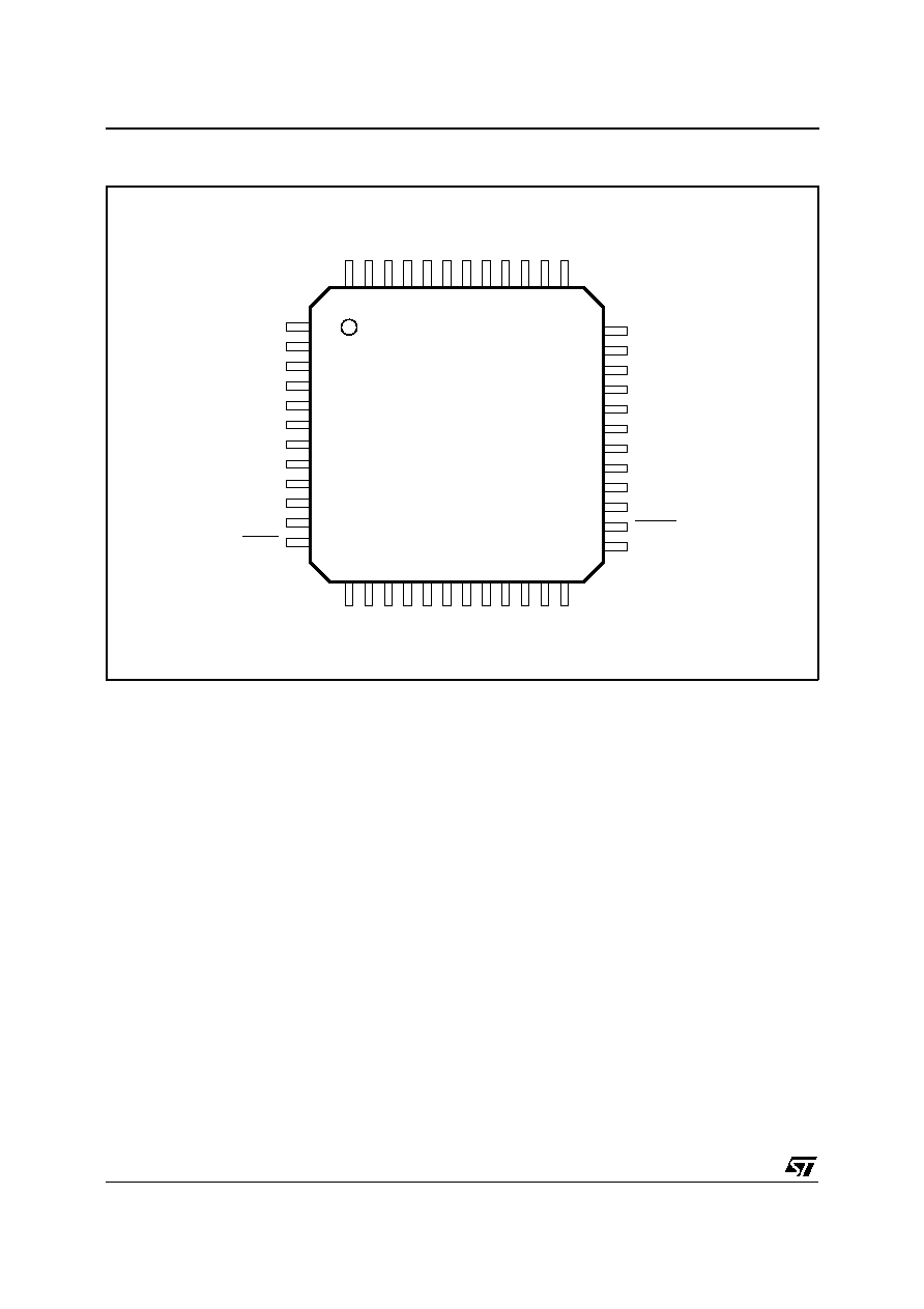
PIN CONNECTIONS
ST7554
2/11

PIN LIST
Name
Pin
Type
Description
XTALIN
9
I
Crystal Input
XTALOUT
10
O
Crystal Output
RESET
12
I
Reset Function to initialise the device (active low)
VBUS
5
I
Positive Voltage Regulator Input, connected to USB VBUS
GNDBUS
3
I
Regulator Ground, connected to USB Ground (0V) (see Note 1)
VREGA
6
I/O
Positive Regulated Analog Input/Output Power Supply
VREGD
4
I/O
Positive Regulated Digital Input/Output Power Supply
PSM
8
I
Power Supply Mode (Bus-powered or Self-powered)
D+
2
I/O
Positive Data Signal of Differential Data Bus conforming to USB Standard
Specification 1.0
D-
1
I/O
Negative Data Signal of Differential Data Bus conforming to USB Standard
Specification 1.0
TRxD
35
I/O
Transmit/Receive Data Led
DC
36
I/O
DC mask
BUZEN
37
I/O
Buzzer Amplifier Enable/Mute
PULSE
38
I/O
Pulse dialing
DISHS
39
I/O
Disconnect external phone
RFC
40
I/O
Refresh
LED
41
I/O
LED control
CD
42
I/O
Carrier Detect Led
CLID
43
I/O
Caller ID
HO
45
I/O
Hook Control
HSDT
46
I/O
Current sense
RI
48
I/O
Ring Indicator
HC1
27
O
Modem Codec Hardware Control mode selection
PDOWN
26
O
SSI Powerdown bit output (active low)
MCLK
29
O
SSI Master Clock Output
DAASEL
34
I
Select Silicon or Discrete DAA Configuration Mode
FS
28
I
SSI Frame Synchronisation Input
DOUT
31
O
SSI Serial Data Output
DIN
30
I
SSI Serial Data Input
FLTPLL
11
OA
PLL filter analog output. Must be connected to analog ground AGND with
33pF capacitor
DGND
32
I
Digital Ground (0V) (see Note 1)
AGND
7
I
Analog Ground (0V) (see Note 1)
RESERVED
13 to 25-33-44
-
Not connected
RESERVED
47
-
Connect to digital ground DGND
Note 1 : Analog and digital ground pins must be tied together to USB ground GNDBUS.
75
54
S
-
0
1
.
T
B
L
ST7554
3/11
PIN DESCRIPTION
1 - Power Supply (7 pins)
1.1 - Regulator Input Power Supply (VBUS)
This pin must be connected to USB VBUS (+5V).
It supplies the integrated analog USB transceiver.
It is also the positive regulator power supply input
(5V) when ST7554 is in bus-powered mode
(PSM = 1) and it is used to internally generate the
3.3V supply for the digital and analog circuitry.
1.2 - Regulated Analog V
DD
Supply (VREGA)
This pin is the analog power supply input (PSM = 0)
or analog 3.3V power supply output (PSM = 1).
This pin is the positive analog power supply for the
external Codec and DAA.
It is recommended to add a 1
µ
F capacitor between
VREGA and GNDA as close as possible to the
IC pins.
1.3 - Regulated V
DD
Supply (VREGD)
This pin is the digital power supply input (PSM = 0)
or digital 3.3V power supply output (PSM = 1).
This pin is the positive digital power supply for the
external Codec and DAA.
It is recommended to add a 1
µ
F capacitor between
VREGA and GNDA as close as possible to the
IC pins.
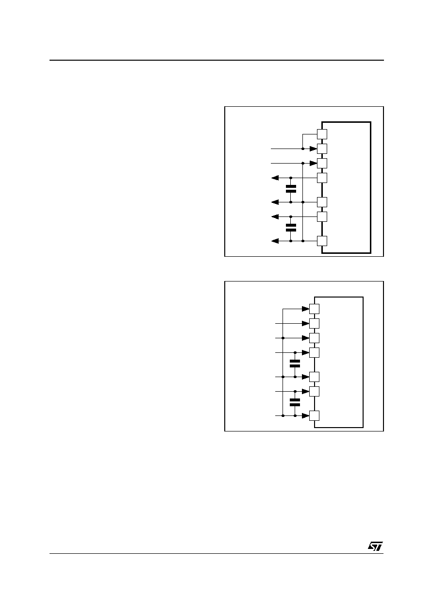
1.4 - Power Supply Mode (PSM)
This pin controls the VREGD and VREGA power
supply mode.
When PSM = 1, the application is bus-powered.
The 3.3V power supply is generated internally from
VBUS. In this case VREGD and VREGA are out-
puts which can be used to supply 3.3V to external
devices (see Figure 1).
When PSM = 0, the application is self-powered.
VBUS must be still connected to the VBUS Pin of
the USB connector in order to supply the integrated
USB transceiver. Anyway in this case VREGD and
VREGA must be fed by a 3.3V externally regulated
digital and analog power supplies (see Figure 2).
1.5 - Ground (DGND, AGND and GNDBUS)
DGND, AGND and GNDBUS are the digital, analog
and USB ground return pins respectively.
They should be connected together outside the
chip to the GND pin of the USB plug.
8 PSM
5 VBUS
3 GNDBUS
4 VREGD
32 DGND
6 VREGA
7 AGND
ST7554
from USB
to other
digital ICs
to other
analog ICs
75
54
S
-
0
2
.
E
P
S
Figure 1 :
ST7554 in Bus-Powered mode
(PSM = 1)
8 PSM
5 VBUS
3 GNDBUS
4 VREGD
32 DGND
6 VREGA
7 AGND
ST7554
from USB
from 3.3V
externally
regulated
supplies
75
54
S
-
0
3.
E
P
S
Figure 2 :
ST7554 in Self Powered mode
(PSM = 0)
2 - USB Interface (D+ , D-)
These pins are the positive and negative USB
differential data lines. They shall be both connected
to the USB plug or USB protection circuit via 27
series resistors for line impedance matching.
ST7554
4/11
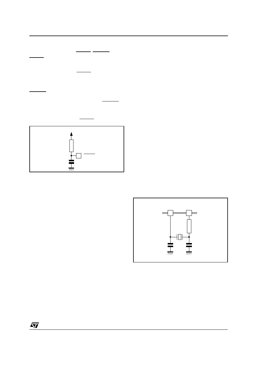
3 - Reset, Powerdown (RESET, PDOWN)
RESET Pin initialises the internal counters and
control registers to their default value. A minimum
low pulse of 1ms is required to reset the chip.
In a typical application RESET is connected to
VBUS through a R, C network. This ensures that
the chip is reset at each connection / disconnection
to the USB bus (see Figure 3).
PDOWN Pin shall be connected to the powerdown
inputs of the external codec used on the SSI.
When ST7554 is in Suspend mode, PDOWN is
forced low so that the external codec is in
powerdown.
PIN DESCRIPTION (continued)
12 RESET
R
220k
W
C
10nF
VBUS
75
54
S
-
0
4
.
E
P
S
Figure 3 : RC network for RESET
9
10
R
1.8k
W
C
18pF
C
18pF
AGND
AGND
XTAL
OUT
XTAL
IN
75
54
S
-
0
5.
E
P
S
Figure 4 :
Application schematic for the
9.216MHz external crystal
4 - Serial Synchronous Interface
ST7554 has a Serial Syncronous Interface (SSI)
dedicated to the connection of the STLC7550 or
ST75951, ST high performance Modem Analog
Front-End (MAFE).
4.1 - Data (DIN, DOUT)
Digital data word input/output of SSI, to be con-
nected to the data word pins of STLC7550 or
ST75951.
4.2 - Master Clock (MCLK)
This pin is the master clock output.
4.3 - Frame Synchronization (FS)
The frame synchronization is used to synchronize data
transfer between ST7554 and the external Codec.
4.4 - Hardware Control (HC1)
HC1 must be connected to the corresponding pin of
STLC7550 or ST75951, while their HC0 Pin shall be
tied to the 3.3V VREGD digital supply. This pin
selects data or control modes for the Modem Codec.
4.5 - DAA Selection (DAASEL)
Connect to VREGD when using silicon DAA chipset
based on ST75951 + ST952. Connect to DGND
when using STLC7550 with discrete interface.
5 - DAA Control Pins (IMP, DC, BUZEN,
PULSE, DISHS, RFC, LED, CLID, HO, HSDT, RI)
These pins control the World Wide software
programmable DAA through ST75951/ST952.
6 - Crystal (XTALIN, XTALOUT)
These pins must be tied to the 9.216MHz external
crystal.
It is recommended to use a
±
50ppm fundamental
parallel resonator crystal. It is recommended to
insert a 1.8k
resistor between XTALOUT and the
crystal to limit its energy to 100
µ
W for a 20
resonator (see Figure 4).
For a SMD crystal the load capacitor is typically
C
LOAD
= 12pF and this leads to an ideal value of
C = 24pF for the capacitors between the crystal
and analog ground (AGND). Anyway, in practice
these capacitors shall be reduced down to
C = 18pF each by considering parasitic capacitors
on PCB and package (see Figure 4).
After a reset or when leaving the suspend state,
the 9.216MHz is asserted inside ST7554 only
3.5ms later in order to wait for it to be stable.
7 - PLL Output Filter (FLTPLL)
This pin must be connected to the analog ground
(AGND) through a 33pF capacitor.
8 - Reserved Pins (18 pins)
These pins must be left not connected except
Pin 47 which should be connected to the digital
ground DGND.
ST7554
5/11