ST75C185
LOW POWER
MULTIPLE RS-232 DRIVERS AND RECEIVERS
TARGET DATA
Æ
June 2000
s
MEETS STANDARD EIA-232-E
s
SINGLE CHIP WITH INTERFACE BETWEEN
UART AND SERIAL PORT CONNECTOR
s
LESS THAN 20mW QUIESCENT POWER
CONSUMPTION
s
WIDE DRIVER SUPPLY VOLTAGE: 7 TO 13.2V
s
DRIVER OUTPUT SLEW RATE LIMITED TO
30V/
µ
s MAX
s
RECEIVER INPUT HYSTERESIS: 1.1 TYP
s
PUSH-PULL RECEIVER OUTPUTS
s
ON CHIP RECEIVER 1
µ
s NOISE FILTER
s
FUNCTIONALLY INTERCHANGEABLE WITH
STM ST75185
s
ESD PROTECTION:
±
10KV HUMAN BODY
MODEL
DESCRIPTION
The ST75C185 is low power BICMOS device
containing three independent drivers and five
receivers that is used to interface data terminal
equipment (DTE) with data circuit-terminating
equipment
(DCE).
This
device
has
been
designed
to
conform
to
Standards
ANSI/EIA-232-E. The drivers have a controlled
output slew rate that is limited to a maximum of
30V/
µ
s and the receivers have filters that reject
input noise pulses that are shorter than 1
µ
s. Both
these features eliminate the need of external
components.
The ST75C185 hasn't a power sequence fault
condition. It has been designed using low-power
techniques in a BICMOS tecnology.
In most application the receivers contained in this
device will interface to single inputs peripheral
devices
such
as
ACEs,
UARTs
or
microprocessors.
By
using
sampling,
such
peripheral devices are usuallly insensitive to the
transition times of the input signals. If this is not
the case, or for other uses, it is recommended
that the ST75C185 receiver outputs be buffered
by single gates of the HCMOS, ALS or 74F logic
families.
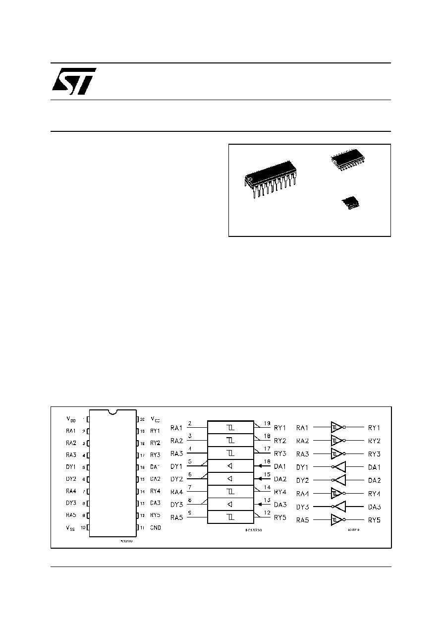
PIN CONNECTION IEC LOGIC SYMBOL AND LOGIC DIAGRAM
(Micro Package)
(Plastic Package)
(TSSOP Package)
1/13
ORDER CODES
T ype
T emperature Ran ge
Package
Comments
ST75C185CN
0 to 70
o
C
DIP-20
20 parts per tube / 50 tubes per box
ST75C185CD
0 to 70
o
C
SO-20 (Tube)
40 parts per tube / 25 tubes per box
ST75C185CDR
0 to 70
o
C
SO-20 (Tape & Reel)
1000 parts per reel
ST75C185CTR
0 to 70
o
C
TSSOP20 (Tape & Reel)
2500 parts per reel
ST75C185BN
-40 to 85
o
C
DIP-20
20 parts per tube / 50 tubes per box
ST75C185BD
-40 to 85
o
C
SO-20 (Tube)
40 parts per tube / 25 tubes per box
ST75C185BDR
-40 to 85
o
C
SO-20 (Tape & Reel)
1000 parts per reel
ST75C185BTR
-40 to 85
o
C
TSSOP20 (Tape & Reel)
2500 parts per reel
PIN DESCRIPTION
PIN No
SYMBOL
NAME AND F UNCTIO N
1
V
DD
Supply Voltage (+12V)
2
RA1
First Receiver Input
3
RA2
Second Receiver Input
4
RA3
Third Receiver Input
5
DY1
First Driver Output
6
DY2
Second Driver Output
7
RA4
FourthReceiver Input
8
DY3
Third Driver Output
9
RA5
Fifth Receiver Input
10
V
SS
Supply Voltage (-12V)
11
GND
Ground
12
RY5
Fifth Receiver Output
13
DA3
Third Driver Input
14
RY4
Fourth Receiver Output
15
DA2
Second Driver Input
16
DA1
First Driver Input
17
RY3
Third Receiver Output
18
RY2
Second Receiver Output
19
RY1
First Receiver Output
20
V
CC
Supply Voltage (+5V)
ST75C185
2/13
ABSOLUTE MAXIMUM RATINGS OVER OPERATING FREE-AIR TEMPERATURE RANGE
(unless otherwise specified)
Symbol
Parameter
Value
Un it
V
DD
Supply Voltage (Note 1)
15
V
V
SS
Supply Voltage (Note 1)
-15
V
V
CC
Supply Voltage (Note 1)
7
V
V
I
Input Voltage Range (DRIVER)
-0.3 to (V
CC
+0.3)
V
V
I
Input Voltage Range (RECEIVER)
-30 to 30
V
V
O
Output Voltage Range (DRIVER)
(V
SS
-6) to (V
DD
+6)
V
V
O
Output Voltage Range (RECEIVER)
-0.3 to (V
CC
+0.3)
V
I
O
Receiver Low Level Output Current
20
mA
T
A
Operating Free-Air Temperature Range
-40 to 85
o
C
T
stg
Storage Temperature Range
-65 to +150
o
C
T
L
Lead Temperature 1.6mm from case for 10 sec
260
o
C
Absolute Maximum Ratings are those values beyond which damage to the device may occur. Functional operation under these condition is not implied.
NOTE1:All voltages are withrespect tothe network ground terminal.
RECOMMENDED OPERATING CONDITIONS
Symbol
Parameter
Min
TYP
Max
Uni t
V
DD
Supply Voltage
7
12
13.2
V
V
SS
Supply Voltage
-7
-12
-13.2
V
V
CC
Supply Voltage
4.5
5
5.5
V
V
IN
Input Voltage (Note 2)
DRIVER
0
V
CC
V
RECEIVER
-25
25
I
OH
High Level Output Current
RECEIVER
-1
mA
I
OL
Low Level Output Current
RECEIVER
3.2
mA
T
A
Operating Free-Air Temperature
-40
25
85
o
C
NOTE 2: The algebraic convertion, where the more positive (less negative) limitis designed as maximum, is used in this datasheet for logic levels only,
e.g. if -10V is a maximum, the typical value is a more negative voltage.
ST75C185
3/13
SUPPLY CURRENTS (V
DD
= 12V, V
SS
= -12V, V
CC
= 5V, unless otherwise specified)
Symb ol
Parameter
T est Cond it ion s
Value
Un it
Min .
T yp.
Max.
I
DD
Supply Current from V
DD
No load. All inputs at 2 or 0.8V
115
500
µ
A
I
SS
Supply Current from V
SS
No load. All inputs at 2 or 0.8V
-115
-500
µ
A
I
CC
Supply Current from V
CC
No load. All inputs at 0 or 5V
950
1500
µ
A
DRIVER ELECTRICAL CHARACTERISTICS OVER OPERATING TEMPERATURE RANGE
(V
DD
= 12V, V
SS
= -12V, V
CC
= 5V
±
10%, unless otherwise specified)
Symb ol
Parameter
T est Cond it ion s
Value
Un it
Min .
T yp.
Max.
V
OH
High Level Output Voltage
V
IL
= 0.8V
R
L
= 3K
(See Figure 1)
V
DD
= 7V, V
SS
= -7V
5
6.3
V
V
DD
= 12V, V
SS
= -12V
10
10.8
V
V
OL
Low Level Output Voltage
(Note 3)
V
IH
= 1.9 V
R
L
= 3K
(See Figure 1)
V
DD
= 7V, V
SS
= -7V
-6.3
-5
V
V
DD
= 12V, V
SS
= -12V
-10.8
-10
V
V
IH
High Level Input Voltage
2
1.4
V
V
IL
Low Level Input Voltage
1.4
0.8
V
I
IH
High Level Input Current
V
I
= 5 V (See Figure 2)
1
µ
A
I
IL
Low Level Input Current
V
I
= 0 V (See Figure 2)
-1
µ
A
I
OS(H)
High Level Short Circuit
Output Current (Note 4)
V
I
= 0.8 V V
O
= 0V or V
SS
(See Figure 1)
-6
-20
-60
mA
I
OS(L)
Low Level Short Circuit
Output Current (Note 4)
V
I
= 2 V V
O
= 0V or V
SS
(See Figure 1)
6
35
60
mA
R
O
Output Resistance
V
O
= -2 to 2 V V
SS
= V
CC
= V
DD
= 0V
300
450
NOTE 3: The algebraic convention, where the more positive (less negative) limitis designated as maximum, is used in this datasheet for logic levels only
(e.g. if -10V is a maximum, the typical value is a more negative voltage).
NOTE 4: Notmore than one outputs should be shorted atone time.
DRIVER SWITCHING CHARACTERISTICS
(V
DD
= 12V, V
SS
= -12V, V
CC
= 5V T
A
= 25
o
C)
Symb ol
Parameter
T est Cond it ion s
Value
Un it
Min .
T yp.
Max.
t
PLH
Propagation Delay Time, Low
to High Level Output
R
L
= 3 to 7 K
C
L
= 1000 pF
(See Figures 3)
1.9
4
µ
s
t
PHL
Propagation Delay Time High
to Low Level Output
R
L
= 3 to 7 K
C
L
= 1000 pF
(See Figures 3)
1.6
4
µ
s
t
TLH
Transition Time Low to High
Level Output
R
L
= 3 to 7 K
C
L
= 1000 pF
(See Figures 3)
0.53
2
3.2
µ
s
t
THL
Transition Time High to Low
Level Output
R
L
= 3 to 7 K
C
L
= 1000 pF
(See Figure 3)
0.53
2
3.2
µ
s
SR
Output Slew Rate (Note 5)
R
L
= 3 to 7 K
C
L
= 50 to 2500 pF
(See Figure 3)
4
11
30
V/
µ
s
NOTE 5: Measured between -3V and 3V points of output waveform (EIA-232-E conditions), all unused inputs tied either high or low.
ST75C185
4/13
RECEIVER ELECTRICAL CHARACTERISTICS OVER OPERATING TEMPERATURE RANGE
(V
DD
= 12V, V
SS
= -12V, V
CC
= 5V
±
10%, unless otherwise specified)
Symb ol
Parameter
T est Cond it ion s
Value
Un it
Min .
T yp.
Max.
V
T+
Positive Going Threshold
Voltage
(See Figure 6)
1.6
2.1
2.55
V
V
T-
Negative Going Threshold
Voltage
(See Figure 6)
0.65
1
1.25
V
V
hys
Input Hysteresis (V
T+
- V
T-
)
(Note 6)
0.6
1.1
V
V
OH
High Level Output Voltage
(Note 7)
I
OH
= 0.75mA or Input Open
I
OH
= -1mA (See Figure 6)
3.5
4.8
V
V
OL
Low Level Output Voltage
V
I
= 3 V
I
OL
= 3.2 mA
(See Figure 6)
0.2
0.4
V
I
IH
High Level Input Current
V
I
= 25 V
(See Figure 6)
3.6
4.5
8.3
mA
V
I
= 3 V
(See Figure 6)
0.43
0.55
1
I
IL
Low Level Input Current
V
I
= -25 V
(See Figure 6)
-3.6
-4.4
-8.3
mA
V
I
= -3 V
(See Figure 6)
-0.4
-0.55
-1
I
OS(H)
Short-Circuit Output Current
at High Level
V
I
= 0.75 V
V
O
= 0 V
(See Figure 5)
-13
-30
mA
I
OS(L)
Short-Circuit Output Current
at Low Level
V
I
= V
CC
V
O
= V
CC
(See Figure 5)
35
60
mA
Alltypical values are at T
A
= 25
o
C,
NOTE 6: Hysteresis is thedifference between the positive going input threshold voltage, V
T+
, and the negative going input threshold voltage V
T-
.
NOTE 7: Ifthe inputs are letf unconnected, the receiver interprets this as an input low, and the receiver outputs will remain in the high state.
RECEIVER SWITCHING CHARACTERISTICS
(V
DD
= 12V, V
SS
= -12V, V
CC
= 5V
±
10% T
A
= 25
o
C)
Symbo l
Parameter
T est Co ndi tio ns
Value
Uni t
Min.
Typ .
Max.
t
PLH
Propagation Delay Time, Low
to High Level Output
R
L
= 5 K
C
L
= 50 pF
(See Figure 6)
3.2
4
µ
s
t
PHL
Propagation Delay Time High
to Low Level Output
R
L
= 5 K
C
L
= 50 pF
(See Figure 6)
2.6
4
µ
s
t
TLH
Transition Time Low to High
Level Output
R
L
= 5 K
C
L
= 50 pF
(See Figure 6)
30
100
ns
t
THL
Transition Time High to Low
Level Output
R
L
= 5 K
C
L
= 50 pF
(See Figure 6)
10
50
ns
t
W(N)
Pulse Duration of longest
pulse rejection as noise
(Note8)
R
L
= 5 K
C
L
= 50 pF
(See Figure 6)
1
2.3
4
µ
s
NOTE 8: The receiver ignores any positive or negative going pulse that is less than the minimumvalue oft
W(N)
and accepts anypositive or negative going
pulse greater than the maximum of t
W(N)
.
ST75C185
5/13