Äîêóìåíòàöèÿ è îïèñàíèÿ www.docs.chipfind.ru
December 2004
1/131
Rev. 2.0
ST7LITE1
8-BIT MCU WITH SINGLE VOLTAGE FLASH MEMORY,
DATA EEPROM, ADC, 4 TIMERS, SPI
Memories
4 Kbytes single voltage extended Flash
(XFlash) Program memory with read-out pro-
tection, In-Circuit Programming and In-Appli-
cation programming (ICP and IAP). 10K write/
erase cycles guaranteed, data retention: 20
years at 55°C.
256 bytes RAM
128 bytes data E
2
PROM with read-out protec-
tion. 300K write/erase cycles guaranteed,
data retention: 20 years at 55°C.
Clock, Reset and Supply Management
Enhanced reset system
Enhanced low voltage supervisor (LVD) for
main supply and an auxiliary voltage detector
(AVD) with interrupt capability for implement-
ing safe power-down procedures
Clock sources: Internal 1% RC oscillator (on
some devices), crystal/ceramic resonator or
external clock
Internal 32-MHz input clock for Auto-reload
timer
Optional x4 or x8 PLL for 4 or 8 MHz internal
clock
Five Power Saving Modes: Halt, Active-Halt,
Auto Wake-up from Halt, Wait and Slow
I/O Ports
Up to 15 multifunctional bidirectional I/O lines
7
high sink outputs
4 Timers
Configurable watchdog timer
Two 8-bit Lite Timers with prescaler,
1 realtime base and 1 input capture
One 12-bit Auto-reload Timer with 4 PWM
outputs, input capture and output compare
functions
Communication Interface
SPI synchronous serial interface
Interrupt Management
10 interrupt vectors plus TRAP and RESET
15 external interrupt lines (on 4 vectors)
A/D Converter
7 input channels
Fixed gain Op-amp
13-bit precision for 0 to 430 mV (@ 5V V
DD
)
10-bit precision for 430 mV to 5V (@ 5V V
DD
)
Instruction Set
8-bit data manipulation
63 basic instructions with illegal opcode de-
tection
17 main addressing modes
8 x 8 unsigned multiply instructions
Development Tools
Full hardware/software development package
DM (Debug Module)
Device Summary
SO20
Features
ST7LITE10
ST7LITE15
ST7LITE19
Program memory - bytes
4K
RAM (stack) - bytes
256 (128)
Data EEPROM - bytes
-
-
128
Peripherals
Lite Timer with Watchdog,
Autoreload Timer, SPI,
10-bit ADC with Op-Amp
Lite Timer with Watchdog,
Autoreload Timer with 32-MHz input clock,
SPI, 10-bit ADC with Op-Amp
Operating Supply
2.4V to 5.5V
CPU Frequency
Up to 8Mhz
(w/ ext OSC up to 16MHz)
Up to 8Mhz (w/ ext OSC up to 16MHz
and int 1MHz RC 1% PLLx8/4MHz)
Operating Temperature
-40°C to +85°C
Packages
SO20 300"
1

Table of Contents
131
2/131
1 INTRODUCTION . . . . . . . . . . . . . . . . . . . . . . . . . . . . . . . . . . . . . . . . . . . . . . . . . . . . . . . . . . . . . . 5
2 PIN DESCRIPTION . . . . . . . . . . . . . . . . . . . . . . . . . . . . . . . . . . . . . . . . . . . . . . . . . . . . . . . . . . . . 6
3 REGISTER & MEMORY MAP . . . . . . . . . . . . . . . . . . . . . . . . . . . . . . . . . . . . . . . . . . . . . . . . . . . 10
4 FLASH PROGRAM MEMORY . . . . . . . . . . . . . . . . . . . . . . . . . . . . . . . . . . . . . . . . . . . . . . . . . . 13
4.1
INTRODUCTION . . . . . . . . . . . . . . . . . . . . . . . . . . . . . . . . . . . . . . . . . . . . . . . . . . . . . . . 13
4.2
MAIN FEATURES . . . . . . . . . . . . . . . . . . . . . . . . . . . . . . . . . . . . . . . . . . . . . . . . . . . . . . 13
4.3
PROGRAMMING MODES . . . . . . . . . . . . . . . . . . . . . . . . . . . . . . . . . . . . . . . . . . . . . . . . 13
4.4
ICC INTERFACE . . . . . . . . . . . . . . . . . . . . . . . . . . . . . . . . . . . . . . . . . . . . . . . . . . . . . . . 14
4.5
MEMORY PROTECTION . . . . . . . . . . . . . . . . . . . . . . . . . . . . . . . . . . . . . . . . . . . . . . . . 15
4.6
RELATED DOCUMENTATION . . . . . . . . . . . . . . . . . . . . . . . . . . . . . . . . . . . . . . . . . . . . 15
4.7
REGISTER DESCRIPTION . . . . . . . . . . . . . . . . . . . . . . . . . . . . . . . . . . . . . . . . . . . . . . . 15
5 DATA EEPROM . . . . . . . . . . . . . . . . . . . . . . . . . . . . . . . . . . . . . . . . . . . . . . . . . . . . . . . . . . . . . 16
5.1
INTRODUCTION . . . . . . . . . . . . . . . . . . . . . . . . . . . . . . . . . . . . . . . . . . . . . . . . . . . . . . . 16
5.2
MAIN FEATURES . . . . . . . . . . . . . . . . . . . . . . . . . . . . . . . . . . . . . . . . . . . . . . . . . . . . . . 16
5.3
MEMORY ACCESS . . . . . . . . . . . . . . . . . . . . . . . . . . . . . . . . . . . . . . . . . . . . . . . . . . . . . 17
5.4
POWER SAVING MODES . . . . . . . . . . . . . . . . . . . . . . . . . . . . . . . . . . . . . . . . . . . . . . . 19
5.5
ACCESS ERROR HANDLING . . . . . . . . . . . . . . . . . . . . . . . . . . . . . . . . . . . . . . . . . . . . 19
5.6
DATA EEPROM READ-OUT PROTECTION . . . . . . . . . . . . . . . . . . . . . . . . . . . . . . . . . 19
5.7
REGISTER DESCRIPTION . . . . . . . . . . . . . . . . . . . . . . . . . . . . . . . . . . . . . . . . . . . . . . . 20
6 CENTRAL PROCESSING UNIT . . . . . . . . . . . . . . . . . . . . . . . . . . . . . . . . . . . . . . . . . . . . . . . . . 21
6.1
INTRODUCTION . . . . . . . . . . . . . . . . . . . . . . . . . . . . . . . . . . . . . . . . . . . . . . . . . . . . . . . 21
6.2
MAIN FEATURES . . . . . . . . . . . . . . . . . . . . . . . . . . . . . . . . . . . . . . . . . . . . . . . . . . . . . . 21
6.3
CPU REGISTERS . . . . . . . . . . . . . . . . . . . . . . . . . . . . . . . . . . . . . . . . . . . . . . . . . . . . . . 21
7 SUPPLY, RESET AND CLOCK MANAGEMENT . . . . . . . . . . . . . . . . . . . . . . . . . . . . . . . . . . . . 24
7.1
INTERNAL RC OSCILLATOR ADJUSTMENT . . . . . . . . . . . . . . . . . . . . . . . . . . . . . . . . 24
7.2
PHASE LOCKED LOOP . . . . . . . . . . . . . . . . . . . . . . . . . . . . . . . . . . . . . . . . . . . . . . . . . 24
7.3
REGISTER DESCRIPTION . . . . . . . . . . . . . . . . . . . . . . . . . . . . . . . . . . . . . . . . . . . . . . . 25
7.4
MULTI-OSCILLATOR (MO) . . . . . . . . . . . . . . . . . . . . . . . . . . . . . . . . . . . . . . . . . . . . . . . 27
7.5
RESET SEQUENCE MANAGER (RSM) . . . . . . . . . . . . . . . . . . . . . . . . . . . . . . . . . . . . . 28
7.6
SYSTEM INTEGRITY MANAGEMENT (SI) . . . . . . . . . . . . . . . . . . . . . . . . . . . . . . . . . . 30
8 INTERRUPTS . . . . . . . . . . . . . . . . . . . . . . . . . . . . . . . . . . . . . . . . . . . . . . . . . . . . . . . . . . . . . . . 35
8.1
NON MASKABLE SOFTWARE INTERRUPT . . . . . . . . . . . . . . . . . . . . . . . . . . . . . . . . . 35
8.2
EXTERNAL INTERRUPTS . . . . . . . . . . . . . . . . . . . . . . . . . . . . . . . . . . . . . . . . . . . . . . . 35
8.3
PERIPHERAL INTERRUPTS . . . . . . . . . . . . . . . . . . . . . . . . . . . . . . . . . . . . . . . . . . . . . 35
9 POWER SAVING MODES . . . . . . . . . . . . . . . . . . . . . . . . . . . . . . . . . . . . . . . . . . . . . . . . . . . . . 39
9.1
INTRODUCTION . . . . . . . . . . . . . . . . . . . . . . . . . . . . . . . . . . . . . . . . . . . . . . . . . . . . . . . 39
9.2
SLOW MODE . . . . . . . . . . . . . . . . . . . . . . . . . . . . . . . . . . . . . . . . . . . . . . . . . . . . . . . . . 39
9.3
WAIT MODE . . . . . . . . . . . . . . . . . . . . . . . . . . . . . . . . . . . . . . . . . . . . . . . . . . . . . . . . . . 40
9.4
HALT MODE . . . . . . . . . . . . . . . . . . . . . . . . . . . . . . . . . . . . . . . . . . . . . . . . . . . . . . . . . . 41
9.5
ACTIVE-HALT MODE . . . . . . . . . . . . . . . . . . . . . . . . . . . . . . . . . . . . . . . . . . . . . . . . . . . 42
9.6
AUTO WAKE UP FROM HALT MODE . . . . . . . . . . . . . . . . . . . . . . . . . . . . . . . . . . . . . . 43
10 I/O PORTS . . . . . . . . . . . . . . . . . . . . . . . . . . . . . . . . . . . . . . . . . . . . . . . . . . . . . . . . . . . . . . . . . 47
1

Table of Contents
3/131
10.1 INTRODUCTION . . . . . . . . . . . . . . . . . . . . . . . . . . . . . . . . . . . . . . . . . . . . . . . . . . . . . . . 47
10.2 FUNCTIONAL DESCRIPTION . . . . . . . . . . . . . . . . . . . . . . . . . . . . . . . . . . . . . . . . . . . . 47
10.3 I/O PORT IMPLEMENTATION . . . . . . . . . . . . . . . . . . . . . . . . . . . . . . . . . . . . . . . . . . . . 50
10.4 UNUSED I/O PINS . . . . . . . . . . . . . . . . . . . . . . . . . . . . . . . . . . . . . . . . . . . . . . . . . . . . . 50
10.5 LOW POWER MODES . . . . . . . . . . . . . . . . . . . . . . . . . . . . . . . . . . . . . . . . . . . . . . . . . . 50
10.6 INTERRUPTS . . . . . . . . . . . . . . . . . . . . . . . . . . . . . . . . . . . . . . . . . . . . . . . . . . . . . . . . . 50
10.7 DEVICE-SPECIFIC I/O PORT CONFIGURATION . . . . . . . . . . . . . . . . . . . . . . . . . . . . . 51
11 ON-CHIP PERIPHERALS . . . . . . . . . . . . . . . . . . . . . . . . . . . . . . . . . . . . . . . . . . . . . . . . . . . . . 52
11.1 WATCHDOG TIMER (WDG) . . . . . . . . . . . . . . . . . . . . . . . . . . . . . . . . . . . . . . . . . . . . . . 52
11.2 12-BIT AUTORELOAD TIMER 2 (AT2) . . . . . . . . . . . . . . . . . . . . . . . . . . . . . . . . . . . . . 56
11.3 LITE TIMER 2 (LT2) . . . . . . . . . . . . . . . . . . . . . . . . . . . . . . . . . . . . . . . . . . . . . . . . . . . . 66
11.4 SERIAL PERIPHERAL INTERFACE (SPI) . . . . . . . . . . . . . . . . . . . . . . . . . . . . . . . . . . . 71
11.5 10-BIT A/D CONVERTER (ADC) . . . . . . . . . . . . . . . . . . . . . . . . . . . . . . . . . . . . . . . . . . 82
12 INSTRUCTION SET . . . . . . . . . . . . . . . . . . . . . . . . . . . . . . . . . . . . . . . . . . . . . . . . . . . . . . . . . 86
12.1 ST7 ADDRESSING MODES . . . . . . . . . . . . . . . . . . . . . . . . . . . . . . . . . . . . . . . . . . . . . . 86
12.2 INSTRUCTION GROUPS . . . . . . . . . . . . . . . . . . . . . . . . . . . . . . . . . . . . . . . . . . . . . . . . 89
13 ELECTRICAL CHARACTERISTICS . . . . . . . . . . . . . . . . . . . . . . . . . . . . . . . . . . . . . . . . . . . . . 92
13.1 PARAMETER CONDITIONS . . . . . . . . . . . . . . . . . . . . . . . . . . . . . . . . . . . . . . . . . . . . . . 92
13.2 ABSOLUTE MAXIMUM RATINGS . . . . . . . . . . . . . . . . . . . . . . . . . . . . . . . . . . . . . . . . . 93
13.3 OPERATING CONDITIONS . . . . . . . . . . . . . . . . . . . . . . . . . . . . . . . . . . . . . . . . . . . . . . 94
13.4 SUPPLY CURRENT CHARACTERISTICS . . . . . . . . . . . . . . . . . . . . . . . . . . . . . . . . . . 100
13.5 CLOCK AND TIMING CHARACTERISTICS . . . . . . . . . . . . . . . . . . . . . . . . . . . . . . . . . 102
13.6 MEMORY CHARACTERISTICS . . . . . . . . . . . . . . . . . . . . . . . . . . . . . . . . . . . . . . . . . . 103
13.7 EMC CHARACTERISTICS . . . . . . . . . . . . . . . . . . . . . . . . . . . . . . . . . . . . . . . . . . . . . . 104
13.8 I/O PORT PIN CHARACTERISTICS . . . . . . . . . . . . . . . . . . . . . . . . . . . . . . . . . . . . . . . 106
13.9 CONTROL PIN CHARACTERISTICS . . . . . . . . . . . . . . . . . . . . . . . . . . . . . . . . . . . . . . 111
13.10 COMMUNICATION INTERFACE CHARACTERISTICS . . . . . . . . . . . . . . . . . . . . . . . . 113
13.11 10-BIT ADC CHARACTERISTICS . . . . . . . . . . . . . . . . . . . . . . . . . . . . . . . . . . . . . . . . 115
14 PACKAGE CHARACTERISTICS . . . . . . . . . . . . . . . . . . . . . . . . . . . . . . . . . . . . . . . . . . . . . . 119
14.1 PACKAGE MECHANICAL DATA . . . . . . . . . . . . . . . . . . . . . . . . . . . . . . . . . . . . . . . . . 119
14.2 SOLDERING AND GLUEABILITY INFORMATION . . . . . . . . . . . . . . . . . . . . . . . . . . . . 121
15 DEVICE CONFIGURATION . . . . . . . . . . . . . . . . . . . . . . . . . . . . . . . . . . . . . . . . . . . . . . . . . . 122
15.1 OPTION BYTES . . . . . . . . . . . . . . . . . . . . . . . . . . . . . . . . . . . . . . . . . . . . . . . . . . . . . . 122
15.2 DEVICE ORDERING INFORMATION . . . . . . . . . . . . . . . . . . . . . . . . . . . . . . . . . . . . . . 124
15.3 DEVELOPMENT TOOLS . . . . . . . . . . . . . . . . . . . . . . . . . . . . . . . . . . . . . . . . . . . . . . . 125
15.4 ST7 APPLICATION NOTES . . . . . . . . . . . . . . . . . . . . . . . . . . . . . . . . . . . . . . . . . . . . . 126
16 IMPORTANT NOTES . . . . . . . . . . . . . . . . . . . . . . . . . . . . . . . . . . . . . . . . . . . . . . . . . . . . . . . 129
16.1 EXECUTION OF BTJX INSTRUCTION . . . . . . . . . . . . . . . . . . . . . . . . . . . . . . . . . . . . 129
16.2 ADC CONVERSION SPURIOUS RESULTS . . . . . . . . . . . . . . . . . . . . . . . . . . . . . . . . . 129
16.3 A/ D CONVERTER ACCURACY FOR FIRST CONVERSION . . . . . . . . . . . . . . . . . . . 129
16.4 NEGATIVE INJECTION IMPACT ON ADC ACCURACY . . . . . . . . . . . . . . . . . . . . . . . 129

ST7LITE1
4/131
16.5 CLEARING ACTIVE INTERRUPTS OUTSIDE INTERRUPT ROUTINE . . . . . . . . . . . . 129
16.6 USING PB4 AS EXTERNAL INTERRUPT . . . . . . . . . . . . . . . . . . . . . . . . . . . . . . . . . . 129
17 REVISION HISTORY . . . . . . . . . . . . . . . . . . . . . . . . . . . . . . . . . . . . . . . . . . . . . . . . . . . . . . . . 130
To obtain the most recent version of this datasheet,
please check at www.st.com>products>technical literature>datasheet
Please also pay special attention to the Section "IMPORTANT NOTES" on page 128.
ST7LITE1
5/131
1 INTRODUCTION
The ST7LITE1 is a member of the ST7 microcon-
troller family. All ST7 devices are based on a com-
mon industry-standard 8-bit core, featuring an en-
hanced instruction set.
The ST7LITE1 features FLASH memory with
byte-by-byte In-Circuit Programming (ICP) and In-
Application Programming (IAP) capability.
Under software control, the ST7LITE1 device can
be placed in WAIT, SLOW, or HALT mode, reduc-
ing power consumption when the application is in
idle or standby state.
The enhanced instruction set and addressing
modes of the ST7 offer both power and flexibility to
software developers, enabling the design of highly
efficient and compact application code. In addition
to standard 8-bit data management, all ST7 micro-
controllers feature true bit manipulation, 8x8 un-
signed multiplication and indirect addressing
modes.
For easy reference, all parametric data are located
in
section 13 on page 91
.The devices feature an
on-chip Debug Module (DM) to support in-circuit
debugging (ICD). For a description of the DM reg-
isters, refer to the ST7 ICC Protocol Reference
Manual.
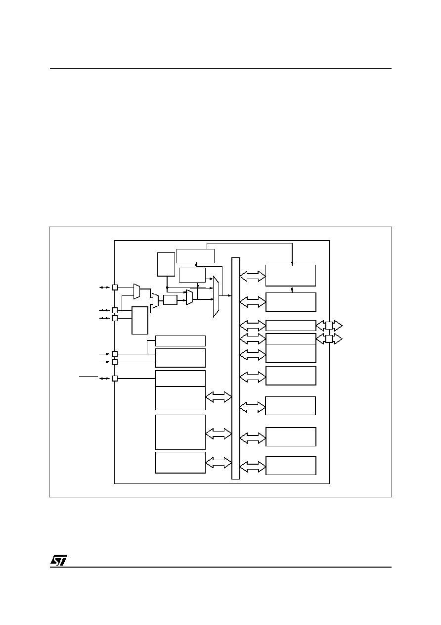
Figure 1. General Block Diagram
8-BIT CORE
ALU
ADDRESS AND DATA BUS
OSC1
OSC2
RESET
PORT A
Internal
CLOCK
CONTROL
RAM
(256 Bytes)
PA7:0
(8 bits)
V
SS
V
DD
POWER
SUPPLY
PROGRAM
(4K Bytes)
LVD
MEMORY
PLL x 8
Ext.
1MHz
PLL
Int.
1MHz
8-Bit
LITE TIMER 2
PORT B
SPI
PB6:0
(7 bits)
DATA EEPROM
(128 Bytes)
1% RC
OSC
to
16MHz
ADC
+ OpAmp
12-Bit
Auto-Reload
TIMER 2
CLKIN
/ 2
or PLL X4
8MHz -> 32MHz
WATCHDOG
Debug Module
1
Document Outline