August 2006
1/135
This is preliminary information on a new product now in development or undergoing evaluation. Details are subject to change without notice.
Rev 1
ST7L1
8-BIT MCU FOR AUTOMOTIVE WITH SINGLE VOLTAGE
FLASH/ROM MEMORY, DATA EEPROM, ADC, 5 TIMERS, SPI
PRELIMINARY DATA
Memories
� 4 Kbytes single voltage extended Flash
(XFlash) or ROM with read-out protection, In-
Circuit programming and In-Application Pro-
gramming (ICP and IAP), 10K write/erase cy-
cles guaranteed, data retention 20 years at
55�C
� 256 bytes RAM
� 128 bytes data E2PROM with read-out pro-
tection, 300K write/erase cycles guaranteed,
data retention 20 years at 55�C
Clock, Reset and Supply Management
� Enhanced reset system
� Enhanced low voltage supervisor (LVD) for
main supply and an auxiliary voltage detector
(AVD) with interrupt capability for implement-
ing safe power-down procedures
� Clock sources: Internal 1% RC oscillator,
crystal/ceramic resonator or external clock
� Optional x4 or x8 PLL for 4 or 8 MHz internal
clock (only x8 PLL available for ROM devices)
� 5 power saving modes: Halt, Active Halt, Auto
Wake-Up from Halt, Wait and Slow
I/O Ports
� Up to 17 multifunctional bidirectional I/O lines
� 7
high sink outputs
5 Timers
� Configurable Watchdog timer
� Two 8-bit Lite timers with prescaler, 1 realtime
base and 1 input capture
� Two 12-bit auto-reload timers with 4 PWM
outputs, 1 input capture, 1 pulse and 4 output
compare functions
Communication Interface
� SPI synchronous serial interface
Interrupt Management
� 12 interrupt vectors plus TRAP and RESET
� 15 external interrupt lines (on 4 vectors)
A/D Converter
� 7 input channels
� 10-bit precision
Instruction Set
� 8-bit data manipulation
� 63 basic instructions with illegal opcode de-
tection
� 17 main addressing modes
� 8 x 8 unsigned multiply instructions
Development Tools
� Full hardware/software development package
� DM (Debug Module)
Device Summary
SO20
300mil
Features
ST7L15
ST7L19
Program memory - bytes
4K
RAM (stack) - bytes
256 (128)
Data EEPROM - bytes
-
128
Peripherals
Lite Timer with Watchdog, Autoreload Timer, SPI, 10-bit ADC
Operating Supply
3V to 5.5V
CPU Frequency
Up to 8 MHz (w/ext OSC up to 16 MHz and int 1 MHz RC 1%, PLLx8/4 MHz)
Operating Temperature
Up to -40 to +85�C / -40 to +125�C
Packages
SO20 300mil
1

Table of Contents
135
2/135
1 INTRODUCTION . . . . . . . . . . . . . . . . . . . . . . . . . . . . . . . . . . . . . . . . . . . . . . . . . . . . . . . . . . . . . . 4
2 PIN DESCRIPTION . . . . . . . . . . . . . . . . . . . . . . . . . . . . . . . . . . . . . . . . . . . . . . . . . . . . . . . . . . . . 5
3 REGISTER AND MEMORY MAP . . . . . . . . . . . . . . . . . . . . . . . . . . . . . . . . . . . . . . . . . . . . . . . . . 7
4 FLASH PROGRAM MEMORY . . . . . . . . . . . . . . . . . . . . . . . . . . . . . . . . . . . . . . . . . . . . . . . . . . 10
4.1
INTRODUCTION . . . . . . . . . . . . . . . . . . . . . . . . . . . . . . . . . . . . . . . . . . . . . . . . . . . . . . . 10
4.2
MAIN FEATURES . . . . . . . . . . . . . . . . . . . . . . . . . . . . . . . . . . . . . . . . . . . . . . . . . . . . . . 10
4.3
PROGRAMMING MODES . . . . . . . . . . . . . . . . . . . . . . . . . . . . . . . . . . . . . . . . . . . . . . . . 10
4.4
ICC INTERFACE . . . . . . . . . . . . . . . . . . . . . . . . . . . . . . . . . . . . . . . . . . . . . . . . . . . . . . . 11
4.5
MEMORY PROTECTION . . . . . . . . . . . . . . . . . . . . . . . . . . . . . . . . . . . . . . . . . . . . . . . . 12
4.6
RELATED DOCUMENTATION . . . . . . . . . . . . . . . . . . . . . . . . . . . . . . . . . . . . . . . . . . . . 12
4.7
REGISTER DESCRIPTION . . . . . . . . . . . . . . . . . . . . . . . . . . . . . . . . . . . . . . . . . . . . . . . 12
5 DATA EEPROM . . . . . . . . . . . . . . . . . . . . . . . . . . . . . . . . . . . . . . . . . . . . . . . . . . . . . . . . . . . . . 13
5.1
INTRODUCTION . . . . . . . . . . . . . . . . . . . . . . . . . . . . . . . . . . . . . . . . . . . . . . . . . . . . . . . 13
5.2
MAIN FEATURES . . . . . . . . . . . . . . . . . . . . . . . . . . . . . . . . . . . . . . . . . . . . . . . . . . . . . . 13
5.3
MEMORY ACCESS . . . . . . . . . . . . . . . . . . . . . . . . . . . . . . . . . . . . . . . . . . . . . . . . . . . . . 14
5.4
POWER SAVING MODES . . . . . . . . . . . . . . . . . . . . . . . . . . . . . . . . . . . . . . . . . . . . . . . 16
5.5
ACCESS ERROR HANDLING . . . . . . . . . . . . . . . . . . . . . . . . . . . . . . . . . . . . . . . . . . . . 16
5.6
DATA EEPROM READ-OUT PROTECTION . . . . . . . . . . . . . . . . . . . . . . . . . . . . . . . . . 16
5.7
REGISTER DESCRIPTION . . . . . . . . . . . . . . . . . . . . . . . . . . . . . . . . . . . . . . . . . . . . . . . 17
6 CENTRAL PROCESSING UNIT . . . . . . . . . . . . . . . . . . . . . . . . . . . . . . . . . . . . . . . . . . . . . . . . . 18
6.1
INTRODUCTION . . . . . . . . . . . . . . . . . . . . . . . . . . . . . . . . . . . . . . . . . . . . . . . . . . . . . . . 18
6.2
MAIN FEATURES . . . . . . . . . . . . . . . . . . . . . . . . . . . . . . . . . . . . . . . . . . . . . . . . . . . . . . 18
6.3
CPU REGISTERS . . . . . . . . . . . . . . . . . . . . . . . . . . . . . . . . . . . . . . . . . . . . . . . . . . . . . . 18
7 SUPPLY, RESET AND CLOCK MANAGEMENT . . . . . . . . . . . . . . . . . . . . . . . . . . . . . . . . . . . . 21
7.1
INTERNAL RC OSCILLATOR ADJUSTMENT . . . . . . . . . . . . . . . . . . . . . . . . . . . . . . . . 21
7.2
PHASE LOCKED LOOP . . . . . . . . . . . . . . . . . . . . . . . . . . . . . . . . . . . . . . . . . . . . . . . . . 22
7.3
REGISTER DESCRIPTION . . . . . . . . . . . . . . . . . . . . . . . . . . . . . . . . . . . . . . . . . . . . . . . 22
7.4
MULTI-OSCILLATOR (MO) . . . . . . . . . . . . . . . . . . . . . . . . . . . . . . . . . . . . . . . . . . . . . . . 24
7.5
RESET SEQUENCE MANAGER (RSM) . . . . . . . . . . . . . . . . . . . . . . . . . . . . . . . . . . . . . 25
7.6
SYSTEM INTEGRITY MANAGEMENT (SI) . . . . . . . . . . . . . . . . . . . . . . . . . . . . . . . . . . 27
8 INTERRUPTS . . . . . . . . . . . . . . . . . . . . . . . . . . . . . . . . . . . . . . . . . . . . . . . . . . . . . . . . . . . . . . . 31
8.1
NON MASKABLE SOFTWARE INTERRUPT . . . . . . . . . . . . . . . . . . . . . . . . . . . . . . . . . 31
8.2
EXTERNAL INTERRUPTS . . . . . . . . . . . . . . . . . . . . . . . . . . . . . . . . . . . . . . . . . . . . . . . 31
8.3
PERIPHERAL INTERRUPTS . . . . . . . . . . . . . . . . . . . . . . . . . . . . . . . . . . . . . . . . . . . . . 31
9 POWER SAVING MODES . . . . . . . . . . . . . . . . . . . . . . . . . . . . . . . . . . . . . . . . . . . . . . . . . . . . . 35
9.1
INTRODUCTION . . . . . . . . . . . . . . . . . . . . . . . . . . . . . . . . . . . . . . . . . . . . . . . . . . . . . . . 35
9.2
SLOW MODE . . . . . . . . . . . . . . . . . . . . . . . . . . . . . . . . . . . . . . . . . . . . . . . . . . . . . . . . . 35
9.3
WAIT MODE . . . . . . . . . . . . . . . . . . . . . . . . . . . . . . . . . . . . . . . . . . . . . . . . . . . . . . . . . . 36
9.4
HALT MODE . . . . . . . . . . . . . . . . . . . . . . . . . . . . . . . . . . . . . . . . . . . . . . . . . . . . . . . . . . 37
9.5
ACTIVE HALT MODE . . . . . . . . . . . . . . . . . . . . . . . . . . . . . . . . . . . . . . . . . . . . . . . . . . . 38
9.6
AUTO WAKE-UP FROM HALT MODE . . . . . . . . . . . . . . . . . . . . . . . . . . . . . . . . . . . . . . 39
10 I/O PORTS . . . . . . . . . . . . . . . . . . . . . . . . . . . . . . . . . . . . . . . . . . . . . . . . . . . . . . . . . . . . . . . . . 43
10.1 INTRODUCTION . . . . . . . . . . . . . . . . . . . . . . . . . . . . . . . . . . . . . . . . . . . . . . . . . . . . . . . 43
10.2 FUNCTIONAL DESCRIPTION . . . . . . . . . . . . . . . . . . . . . . . . . . . . . . . . . . . . . . . . . . . . 43
10.3 I/O PORT IMPLEMENTATION . . . . . . . . . . . . . . . . . . . . . . . . . . . . . . . . . . . . . . . . . . . . 47
1

Table of Contents
3/135
10.4 UNUSED I/O PINS . . . . . . . . . . . . . . . . . . . . . . . . . . . . . . . . . . . . . . . . . . . . . . . . . . . . . 47
10.5 LOW-POWER MODES . . . . . . . . . . . . . . . . . . . . . . . . . . . . . . . . . . . . . . . . . . . . . . . . . . 47
10.6 INTERRUPTS . . . . . . . . . . . . . . . . . . . . . . . . . . . . . . . . . . . . . . . . . . . . . . . . . . . . . . . . . 47
10.7 DEVICE-SPECIFIC I/O PORT CONFIGURATION . . . . . . . . . . . . . . . . . . . . . . . . . . . . . 48
10.8 MULTIPLEXED INPUT/OUTPUT PORTS . . . . . . . . . . . . . . . . . . . . . . . . . . . . . . . . . . . . 49
11 ON-CHIP PERIPHERALS . . . . . . . . . . . . . . . . . . . . . . . . . . . . . . . . . . . . . . . . . . . . . . . . . . . . . 50
11.1 WATCHDOG TIMER (WDG) . . . . . . . . . . . . . . . . . . . . . . . . . . . . . . . . . . . . . . . . . . . . . . 50
11.2 DUAL 12-BIT AUTORELOAD TIMER 3 (AT3) . . . . . . . . . . . . . . . . . . . . . . . . . . . . . . . . 52
11.3 LITE TIMER 2 (LT2) . . . . . . . . . . . . . . . . . . . . . . . . . . . . . . . . . . . . . . . . . . . . . . . . . . . . 72
11.4 SERIAL PERIPHERAL INTERFACE (SPI) . . . . . . . . . . . . . . . . . . . . . . . . . . . . . . . . . . . 76
11.5 10-BIT A/D CONVERTER (ADC) . . . . . . . . . . . . . . . . . . . . . . . . . . . . . . . . . . . . . . . . . . 88
12 INSTRUCTION SET . . . . . . . . . . . . . . . . . . . . . . . . . . . . . . . . . . . . . . . . . . . . . . . . . . . . . . . . . 92
12.1 ST7 ADDRESSING MODES . . . . . . . . . . . . . . . . . . . . . . . . . . . . . . . . . . . . . . . . . . . . . . 92
12.2 INSTRUCTION GROUPS . . . . . . . . . . . . . . . . . . . . . . . . . . . . . . . . . . . . . . . . . . . . . . . . 95
13 ELECTRICAL CHARACTERISTICS . . . . . . . . . . . . . . . . . . . . . . . . . . . . . . . . . . . . . . . . . . . . . 98
13.1 PARAMETER CONDITIONS . . . . . . . . . . . . . . . . . . . . . . . . . . . . . . . . . . . . . . . . . . . . . . 98
13.2 ABSOLUTE MAXIMUM RATINGS . . . . . . . . . . . . . . . . . . . . . . . . . . . . . . . . . . . . . . . . . 99
13.3 OPERATING CONDITIONS . . . . . . . . . . . . . . . . . . . . . . . . . . . . . . . . . . . . . . . . . . . . . 100
13.4 SUPPLY CURRENT CHARACTERISTICS . . . . . . . . . . . . . . . . . . . . . . . . . . . . . . . . . . 106
13.5 CLOCK AND TIMING CHARACTERISTICS . . . . . . . . . . . . . . . . . . . . . . . . . . . . . . . . . 108
13.6 MEMORY CHARACTERISTICS . . . . . . . . . . . . . . . . . . . . . . . . . . . . . . . . . . . . . . . . . . 110
13.7 EMC CHARACTERISTICS . . . . . . . . . . . . . . . . . . . . . . . . . . . . . . . . . . . . . . . . . . . . . . 111
13.8 I/O PORT PIN CHARACTERISTICS . . . . . . . . . . . . . . . . . . . . . . . . . . . . . . . . . . . . . . . 113
13.9 CONTROL PIN CHARACTERISTICS . . . . . . . . . . . . . . . . . . . . . . . . . . . . . . . . . . . . . . 118
13.10 COMMUNICATION INTERFACE CHARACTERISTICS . . . . . . . . . . . . . . . . . . . . . . . . 120
13.11 10-BIT ADC CHARACTERISTICS . . . . . . . . . . . . . . . . . . . . . . . . . . . . . . . . . . . . . . . . 122
14 PACKAGE CHARACTERISTICS . . . . . . . . . . . . . . . . . . . . . . . . . . . . . . . . . . . . . . . . . . . . . . 124
14.1 PACKAGE MECHANICAL DATA . . . . . . . . . . . . . . . . . . . . . . . . . . . . . . . . . . . . . . . . . 124
14.2 SOLDERING INFORMATION . . . . . . . . . . . . . . . . . . . . . . . . . . . . . . . . . . . . . . . . . . . . 125
15 DEVICE CONFIGURATION AND ORDERING INFORMATION . . . . . . . . . . . . . . . . . . . . . . . 126
15.1 OPTION BYTES . . . . . . . . . . . . . . . . . . . . . . . . . . . . . . . . . . . . . . . . . . . . . . . . . . . . . . 126
15.2 DEVICE ORDERING INFORMATION . . . . . . . . . . . . . . . . . . . . . . . . . . . . . . . . . . . . . . 128
15.3 DEVELOPMENT TOOLS . . . . . . . . . . . . . . . . . . . . . . . . . . . . . . . . . . . . . . . . . . . . . . . 130
15.4 ST7 APPLICATION NOTES . . . . . . . . . . . . . . . . . . . . . . . . . . . . . . . . . . . . . . . . . . . . . 131
16 REVISION HISTORY . . . . . . . . . . . . . . . . . . . . . . . . . . . . . . . . . . . . . . . . . . . . . . . . . . . . . . . . 134
ST7L1
4/135
1 INTRODUCTION
The ST7L1 is a member of the ST7 microcontroller
family suitable for automotive applications. All ST7
devices are based on a common industry-stand-
ard 8-bit core, featuring an enhanced instruction
set.
The ST7L1 features FLASH memory with byte-by-
byte In-Circuit Programming (ICP) and In-Applica-
tion Programming (IAP) capability.
Under software control, the ST7L1 device can be
placed in WAIT, SLOW or HALT mode, reducing
power consumption when the application is in idle
or standby state.
The enhanced instruction set and addressing
modes of the ST7 offer both power and flexibility to
software developers, enabling the design of highly
efficient and compact application code. In addition
to standard 8-bit data management, all ST7 micro-
controllers feature true bit manipulation, 8x8 un-
signed multiplication and indirect addressing
modes.
For easy reference, all parametric data is located
in
section 13 on page 98
. The ST7L1 features an
on-chip Debug Module (DM) to support In-Circuit
Debugging (ICD). For a description of the DM reg-
isters, refer to the ST7 ICC Protocol Reference
Manual.
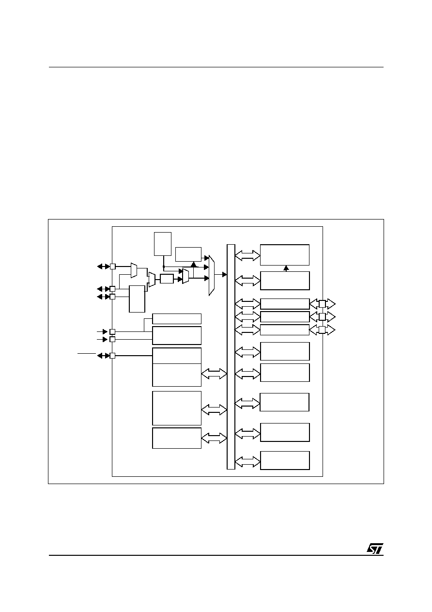
Figure 1. General Block Diagram
*Note: Not available on ROM devices.
8-bit CORE
ALU
ADDRESS AND DATA BUS
OSC1
OSC2
RESET
PORT A
INTERNAL
CLOCK
CONTROL
RAM
(256 bytes)
PA7:0
(8 bits)
V
SS
V
DD
POWER
SUPPLY
PROGRAM
(up to 4 Kbytes)
LVD, AVD
MEMORY
PLL x8
Ext.
1 MHz
Int.
1 MHz
8-bit
LITE TIMER 2
PORT B
SPI
PB6:0
(7 bits)
DATA EEPROM
(128 bytes)
1% RC
OSC
to
16 MHz
ADC
12-bit
AUTO-RELOAD
TIMER 2
CLKIN
/ 2
or PLL x4*
WATCHDOG
DEBUG MODULE
PORT C
PC1:0
(2 bits)
1
ST7L1
5/135
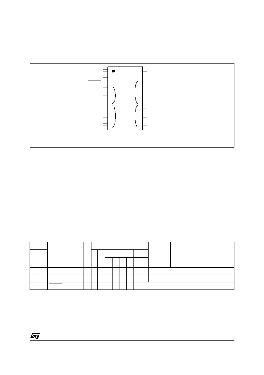
2 PIN DESCRIPTION
Figure 2. 20-Pin SO Package Pinout
Notes:
1. This pin cannot be configured as external interrupt in ROM devices.
2. OSC1 and OSC2 are not multiplexed in ROM devices and Port C is not present.
Legend / Abbreviations for
Table 1
:
Type:
I = input, O = output, S = supply
In/Output level: C
T
= CMOS 0.3V
DD
/ 0.7V
DD
with input trigger
Output level:
HS = 20mA high sink (on N-buffer only)
Port and control configuration:
� Input:
float = floating, wpu = weak pull-up, int = interrupt, ana = analog
� Output:
OD = open drain, PP = push-pull
The RESET configuration of each pin (shown in bold) is valid as long as the device is in reset state.
Table 1. Device Pin Description
20
19
18
17
16
15
14
13
1
2
3
4
5
6
7
8
V
SS
V
DD
AIN5/PB5
CLKIN/AIN4/PB4
MOSI/AIN3/PB3
MISO/AIN2/PB2
SCK/AIN1/PB1
SS/AIN0/PB0
OSC1/CLKIN/PC0
2)
OSC2/PC1
2)
PA5 (HS)/ATPWM3/ICCDATA
PA4 (HS)/ATPWM2
PA3 (HS)/ATPWM1
PA2 (HS)/ATPWM0
PA1 (HS)/ATIC
PA0 (HS)/LTIC
1)
(HS) 20mA High sink capability
eix
associated external interrupt vector
12
11
9
10
AIN6/PB6
PA7 (HS)
PA6/MCO/ICCCLK/BREAK
RESET
ei3
ei2
ei0
ei1
Pin No.
Pin Name
Type
Level
Port / Control
Main
Function
(after
reset)
Alternate Function
SO20
Input
Output
Input
Output
fl
oat
wpu
int
ana
OD
PP
1
V
SS
S Ground
2
V
DD
S
Main power supply
3
RESET I/O
C
T
X
X
Top priority non maskable interrupt (active low)
1