
August 2003
1/122
Rev. 2.4
ST7LITE0, ST7SUPERLITE
8-BIT MCU WITH SINGLE VOLTAGE FLASH MEMORY,
DATA EEPROM, ADC, TIMERS, SPI
s
Memories
≠ 1K or 1.5K bytes single voltage Flash Pro-
gram memory with read-out protection, In-Cir-
cuit and In-Application Programming (ICP and
IAP). 10K write/erase cycles guaranteed, data
retention: 20 years at 55∞C.
≠ 128 bytes RAM.
≠ 128 bytes data EEPROM with read-out pro-
tection. 300K write/erase cycles guaranteed,
data retention: 20 years at 55∞C.
s
Clock, Reset and Supply Management
≠ 3-level low voltage supervisor (LVD) and aux-
iliary voltage detector (AVD) for safe power-
on/off procedures
≠ Clock sources: internal 1MHz RC 1% oscilla-
tor or external clock
≠ PLL x4 or x8 for 4 or 8 MHz internal clock
≠ Four Power Saving Modes: Halt, Active-Halt,
Wait and Slow
s
Interrupt Management
≠ 10 interrupt vectors plus TRAP and RESET
≠ 4 external interrupt lines (on 4 vectors)
s
I/O Ports
≠ 13 multifunctional bidirectional I/O lines
≠ 9 alternate function lines
≠ 6 high sink outputs
s
2 Timers
≠ One 8-bit Lite Timer (LT) with prescaler in-
cluding: watchdog, 1 realtime base and 1 in-
put capture.
≠ One 12-bit Auto-reload Timer (AT) with output
compare function and PWM
s
1 Communication Interface
≠ SPI synchronous serial interface
s
A/D Converter
≠ 8-bit resolution for 0 to V
DD
≠ Fixed gain Op-amp for 11-bit resolution in 0 to
250 mV range (@ 5V V
DD
)
≠ 5 input channels
s
Instruction Set
≠ 8-bit data manipulation
≠ 63 basic instructions
≠ 17 main addressing modes
≠ 8 x 8 unsigned multiply instruction
s
Development Tools
≠ Full hardware/software development package
Device Summary
DIP16
SO16
150"
Features
ST7SUPERLITE
ST7LITE0
ST7LITES2
ST7LITES5
ST7LITE02
ST7LITE05
ST7LITE09
Program memory - bytes
1K
1K
1.5K
1.5K
1.5K
RAM (stack) - bytes
128 (64)
128 (64)
128 (64)
128 (64)
128 (64)
Data EEPROM - bytes
-
-
-
-
128
Peripherals
LT Timer w/ Wdg,
AT Timer w/ 1 PWM,
SPI
LT Timer w/ Wdg,
AT Timer w/ 1 PWM,
SPI, 8-bit ADC
LT Timer w/ Wdg,
AT Timer w/ 1 PWM,
SPI
LT Timer w/ Wdg,
AT Timer w/ 1 PWM, SPI,
8-bit ADC w/ Op-Amp
Operating Supply
2.4V to 5.5V
CPU Frequency
1MHz RC 1% + PLLx4/8MHz
Operating Temperature
-40∞C to +85∞C
Packages
SO16 150", DIP16
1

Table of Contents
122
2/122
ST7LITE0, ST7SUPERLITE . . . . . . . . . . . . . . . . . . . . . . . . . . . . . 1
1 INTRODUCTION . . . . . . . . . . . . . . . . . . . . . . . . . . . . . . . . . . . . . . . . . . . . . . . . . . . . . . . . . . . . . . 5
2 PIN DESCRIPTION . . . . . . . . . . . . . . . . . . . . . . . . . . . . . . . . . . . . . . . . . . . . . . . . . . . . . . . . . . . . 6
3 REGISTER & MEMORY MAP . . . . . . . . . . . . . . . . . . . . . . . . . . . . . . . . . . . . . . . . . . . . . . . . . . . . 8
4 FLASH PROGRAM MEMORY . . . . . . . . . . . . . . . . . . . . . . . . . . . . . . . . . . . . . . . . . . . . . . . . . . 12
4.1
INTRODUCTION . . . . . . . . . . . . . . . . . . . . . . . . . . . . . . . . . . . . . . . . . . . . . . . . . . . . . . . 12
4.2
MAIN FEATURES . . . . . . . . . . . . . . . . . . . . . . . . . . . . . . . . . . . . . . . . . . . . . . . . . . . . . . 12
4.3
PROGRAMMING MODES . . . . . . . . . . . . . . . . . . . . . . . . . . . . . . . . . . . . . . . . . . . . . . . . 12
4.4
ICC INTERFACE . . . . . . . . . . . . . . . . . . . . . . . . . . . . . . . . . . . . . . . . . . . . . . . . . . . . . . . 13
4.5
MEMORY PROTECTION . . . . . . . . . . . . . . . . . . . . . . . . . . . . . . . . . . . . . . . . . . . . . . . . 14
4.6
RELATED DOCUMENTATION . . . . . . . . . . . . . . . . . . . . . . . . . . . . . . . . . . . . . . . . . . . . 14
4.7
REGISTER DESCRIPTION . . . . . . . . . . . . . . . . . . . . . . . . . . . . . . . . . . . . . . . . . . . . . . . 14
5 DATA EEPROM . . . . . . . . . . . . . . . . . . . . . . . . . . . . . . . . . . . . . . . . . . . . . . . . . . . . . . . . . . . . . 15
5.1
INTRODUCTION . . . . . . . . . . . . . . . . . . . . . . . . . . . . . . . . . . . . . . . . . . . . . . . . . . . . . . . 15
5.2
MAIN FEATURES . . . . . . . . . . . . . . . . . . . . . . . . . . . . . . . . . . . . . . . . . . . . . . . . . . . . . . 15
5.3
MEMORY ACCESS . . . . . . . . . . . . . . . . . . . . . . . . . . . . . . . . . . . . . . . . . . . . . . . . . . . . . 16
5.4
POWER SAVING MODES . . . . . . . . . . . . . . . . . . . . . . . . . . . . . . . . . . . . . . . . . . . . . . . 18
5.5
ACCESS ERROR HANDLING . . . . . . . . . . . . . . . . . . . . . . . . . . . . . . . . . . . . . . . . . . . . 18
5.6
DATA EEPROM READ-OUT PROTECTION . . . . . . . . . . . . . . . . . . . . . . . . . . . . . . . . . 18
5.7
REGISTER DESCRIPTION . . . . . . . . . . . . . . . . . . . . . . . . . . . . . . . . . . . . . . . . . . . . . . . 19
6 CENTRAL PROCESSING UNIT . . . . . . . . . . . . . . . . . . . . . . . . . . . . . . . . . . . . . . . . . . . . . . . . . 20
6.1
INTRODUCTION . . . . . . . . . . . . . . . . . . . . . . . . . . . . . . . . . . . . . . . . . . . . . . . . . . . . . . . 20
6.2
MAIN FEATURES . . . . . . . . . . . . . . . . . . . . . . . . . . . . . . . . . . . . . . . . . . . . . . . . . . . . . . 20
6.3
CPU REGISTERS . . . . . . . . . . . . . . . . . . . . . . . . . . . . . . . . . . . . . . . . . . . . . . . . . . . . . . 20
7 SUPPLY, RESET AND CLOCK MANAGEMENT . . . . . . . . . . . . . . . . . . . . . . . . . . . . . . . . . . . . 23
7.1
INTERNAL RC OSCILLATOR ADJUSTMENT . . . . . . . . . . . . . . . . . . . . . . . . . . . . . . . . 23
7.2
PHASE LOCKED LOOP . . . . . . . . . . . . . . . . . . . . . . . . . . . . . . . . . . . . . . . . . . . . . . . . . 23
7.3
REGISTER DESCRIPTION . . . . . . . . . . . . . . . . . . . . . . . . . . . . . . . . . . . . . . . . . . . . . . . 24
7.4
RESET SEQUENCE MANAGER (RSM) . . . . . . . . . . . . . . . . . . . . . . . . . . . . . . . . . . . . . 26
7.5
SYSTEM INTEGRITY MANAGEMENT (SI) . . . . . . . . . . . . . . . . . . . . . . . . . . . . . . . . . . 28
8 INTERRUPTS . . . . . . . . . . . . . . . . . . . . . . . . . . . . . . . . . . . . . . . . . . . . . . . . . . . . . . . . . . . . . . . 33
8.1
NON MASKABLE SOFTWARE INTERRUPT . . . . . . . . . . . . . . . . . . . . . . . . . . . . . . . . . 33
8.2
EXTERNAL INTERRUPTS . . . . . . . . . . . . . . . . . . . . . . . . . . . . . . . . . . . . . . . . . . . . . . . 33
8.3
PERIPHERAL INTERRUPTS . . . . . . . . . . . . . . . . . . . . . . . . . . . . . . . . . . . . . . . . . . . . . 33
9 POWER SAVING MODES . . . . . . . . . . . . . . . . . . . . . . . . . . . . . . . . . . . . . . . . . . . . . . . . . . . . . 36
9.1
INTRODUCTION . . . . . . . . . . . . . . . . . . . . . . . . . . . . . . . . . . . . . . . . . . . . . . . . . . . . . . . 36
9.2
SLOW MODE . . . . . . . . . . . . . . . . . . . . . . . . . . . . . . . . . . . . . . . . . . . . . . . . . . . . . . . . . 36
9.3
WAIT MODE . . . . . . . . . . . . . . . . . . . . . . . . . . . . . . . . . . . . . . . . . . . . . . . . . . . . . . . . . . 37
9.4
ACTIVE-HALT AND HALT MODES . . . . . . . . . . . . . . . . . . . . . . . . . . . . . . . . . . . . . . . . 38
2

Table of Contents
3/122
10 I/O PORTS . . . . . . . . . . . . . . . . . . . . . . . . . . . . . . . . . . . . . . . . . . . . . . . . . . . . . . . . . . . . . . . . . 41
10.1 INTRODUCTION . . . . . . . . . . . . . . . . . . . . . . . . . . . . . . . . . . . . . . . . . . . . . . . . . . . . . . . 41
10.2 FUNCTIONAL DESCRIPTION . . . . . . . . . . . . . . . . . . . . . . . . . . . . . . . . . . . . . . . . . . . . 41
10.3 UNUSED I/O PINS . . . . . . . . . . . . . . . . . . . . . . . . . . . . . . . . . . . . . . . . . . . . . . . . . . . . . 44
10.4 LOW POWER MODES . . . . . . . . . . . . . . . . . . . . . . . . . . . . . . . . . . . . . . . . . . . . . . . . . . 44
10.5 INTERRUPTS . . . . . . . . . . . . . . . . . . . . . . . . . . . . . . . . . . . . . . . . . . . . . . . . . . . . . . . . . 44
10.6 I/O PORT IMPLEMENTATION . . . . . . . . . . . . . . . . . . . . . . . . . . . . . . . . . . . . . . . . . . . . 44
11 ON-CHIP PERIPHERALS . . . . . . . . . . . . . . . . . . . . . . . . . . . . . . . . . . . . . . . . . . . . . . . . . . . . . 46
11.1 LITE TIMER (LT) . . . . . . . . . . . . . . . . . . . . . . . . . . . . . . . . . . . . . . . . . . . . . . . . . . . . . . . 46
11.2 12-BIT AUTORELOAD TIMER (AT) . . . . . . . . . . . . . . . . . . . . . . . . . . . . . . . . . . . . . . . . 51
11.3 SERIAL PERIPHERAL INTERFACE (SPI) . . . . . . . . . . . . . . . . . . . . . . . . . . . . . . . . . . . 57
11.4 8-BIT A/D CONVERTER (ADC) . . . . . . . . . . . . . . . . . . . . . . . . . . . . . . . . . . . . . . . . . . . 68
12 INSTRUCTION SET . . . . . . . . . . . . . . . . . . . . . . . . . . . . . . . . . . . . . . . . . . . . . . . . . . . . . . . . . 72
12.1 ST7 ADDRESSING MODES . . . . . . . . . . . . . . . . . . . . . . . . . . . . . . . . . . . . . . . . . . . . . . 72
12.2 INSTRUCTION GROUPS . . . . . . . . . . . . . . . . . . . . . . . . . . . . . . . . . . . . . . . . . . . . . . . . 75
13 ELECTRICAL CHARACTERISTICS . . . . . . . . . . . . . . . . . . . . . . . . . . . . . . . . . . . . . . . . . . . . . 78
13.1 PARAMETER CONDITIONS . . . . . . . . . . . . . . . . . . . . . . . . . . . . . . . . . . . . . . . . . . . . . . 78
13.2 ABSOLUTE MAXIMUM RATINGS . . . . . . . . . . . . . . . . . . . . . . . . . . . . . . . . . . . . . . . . . 79
13.3 OPERATING CONDITIONS . . . . . . . . . . . . . . . . . . . . . . . . . . . . . . . . . . . . . . . . . . . . . . 80
13.4 SUPPLY CURRENT CHARACTERISTICS . . . . . . . . . . . . . . . . . . . . . . . . . . . . . . . . . . . 86
13.5 CLOCK AND TIMING CHARACTERISTICS . . . . . . . . . . . . . . . . . . . . . . . . . . . . . . . . . . 88
13.6 MEMORY CHARACTERISTICS . . . . . . . . . . . . . . . . . . . . . . . . . . . . . . . . . . . . . . . . . . . 89
13.7 EMC CHARACTERISTICS . . . . . . . . . . . . . . . . . . . . . . . . . . . . . . . . . . . . . . . . . . . . . . . 90
13.8 I/O PORT PIN CHARACTERISTICS . . . . . . . . . . . . . . . . . . . . . . . . . . . . . . . . . . . . . . . . 94
13.9 CONTROL PIN CHARACTERISTICS . . . . . . . . . . . . . . . . . . . . . . . . . . . . . . . . . . . . . . . 99
13.10 COMMUNICATION INTERFACE CHARACTERISTICS . . . . . . . . . . . . . . . . . . . . . . . . 100
13.11 8-BIT ADC CHARACTERISTICS . . . . . . . . . . . . . . . . . . . . . . . . . . . . . . . . . . . . . . . . . 102
14 PACKAGE CHARACTERISTICS . . . . . . . . . . . . . . . . . . . . . . . . . . . . . . . . . . . . . . . . . . . . . . 106
14.1 PACKAGE MECHANICAL DATA . . . . . . . . . . . . . . . . . . . . . . . . . . . . . . . . . . . . . . . . . 106
14.2 THERMAL CHARACTERISTICS . . . . . . . . . . . . . . . . . . . . . . . . . . . . . . . . . . . . . . . . . . 107
14.3 SOLDERING AND GLUEABILITY INFORMATION . . . . . . . . . . . . . . . . . . . . . . . . . . . . 108
15 DEVICE CONFIGURATION AND ORDERING INFORMATION . . . . . . . . . . . . . . . . . . . . . . . 109
15.1 OPTION BYTES . . . . . . . . . . . . . . . . . . . . . . . . . . . . . . . . . . . . . . . . . . . . . . . . . . . . . . 109
15.2 DEVICE ORDERING INFORMATION AND TRANSFER OF CUSTOMER CODE . . . . 111
15.3 DEVELOPMENT TOOLS . . . . . . . . . . . . . . . . . . . . . . . . . . . . . . . . . . . . . . . . . . . . . . . 113
15.4 ST7 APPLICATION NOTES . . . . . . . . . . . . . . . . . . . . . . . . . . . . . . . . . . . . . . . . . . . . . 114
16 IMPORTANT NOTES . . . . . . . . . . . . . . . . . . . . . . . . . . . . . . . . . . . . . . . . . . . . . . . . . . . . . . . 116
16.1 EXECUTION OF BTJX INSTRUCTION . . . . . . . . . . . . . . . . . . . . . . . . . . . . . . . . . . . . 116
16.2 IN-CIRCUIT PROGRAMMING OF DEVICES PREVIOUSLY PROGRAMMED WITH HARD-
WARE WATCHDOG OPTION 116
16.3 IN-CIRCUIT DEBUGGING WITH HARDWARE WATCHDOG . . . . . . . . . . . . . . . . . . . 116
17 SUMMARY OF CHANGES . . . . . . . . . . . . . . . . . . . . . . . . . . . . . . . . . . . . . . . . . . . . . . . . . . 117
3

Table of Contents
4/122
ERRATA SHEET . . . . . . . . . . . . . . . . . . . . . . . . . . . . . . . . . . . 118
18 SILICON IDENTIFICATION . . . . . . . . . . . . . . . . . . . . . . . . . . . . . . . . . . . . . . . . . . . . . . . . . . . 118
19 REFERENCE SPECIFICATION . . . . . . . . . . . . . . . . . . . . . . . . . . . . . . . . . . . . . . . . . . . . . . . 118
20 SILICON limitations . . . . . . . . . . . . . . . . . . . . . . . . . . . . . . . . . . . . . . . . . . . . . . . . . . . . . . . . 118
20.1 NEGATIVE INJECTION IMPACT ON ADC ACCURACY . . . . . . . . . . . . . . . . . . . . . . . 118
20.2 ADC CONVERSION SPURIOUS RESULTS . . . . . . . . . . . . . . . . . . . . . . . . . . . . . . . . . 119
20.3 FUNCTIONAL ESD SENSITIVITY . . . . . . . . . . . . . . . . . . . . . . . . . . . . . . . . . . . . . . . . 119
21 Device Marking . . . . . . . . . . . . . . . . . . . . . . . . . . . . . . . . . . . . . . . . . . . . . . . . . . . . . . . . . . . . 120
22 ERRATA SHEET REVISION History . . . . . . . . . . . . . . . . . . . . . . . . . . . . . . . . . . . . . . . . . . . 121
To obtain the most recent version of this datasheet,
please check at www.st.com>products>technical literature>datasheet
Please note that an errata sheet can be found at the end of this document on
page 118
and pay special attention to the Section "IMPORTANT NOTES" on page 116.
1
ST7LITE0, ST7SUPERLITE
5/122
1 INTRODUCTION
The ST7LITE0 and ST7SUPERLITE are members
of the ST7 microcontroller family. All ST7 devices
are based on a common industry-standard 8-bit
core, featuring an enhanced instruction set.
The ST7LITE0 and ST7SUPERLITE feature
FLASH memory with byte-by-byte In-Circuit Pro-
gramming (ICP) and In-Application Programming
(IAP) capability.
Under software control, the ST7LITE0 and
ST7SUPERLITE devices can be placed in WAIT,
SLOW, or HALT mode, reducing power consump-
tion when the application is in idle or standby state.
The enhanced instruction set and addressing
modes of the ST7 offer both power and flexibility to
software developers, enabling the design of highly
efficient and compact application code. In addition
to standard 8-bit data management, all ST7 micro-
controllers feature true bit manipulation, 8x8 un-
signed multiplication and indirect addressing
modes.
For easy reference, all parametric data are located
in
section 13 on page 78
.
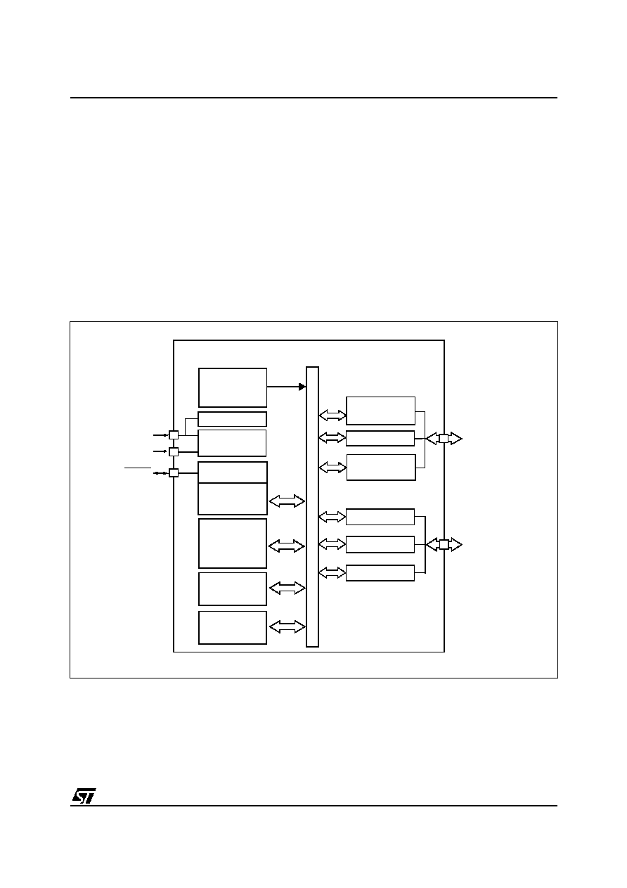
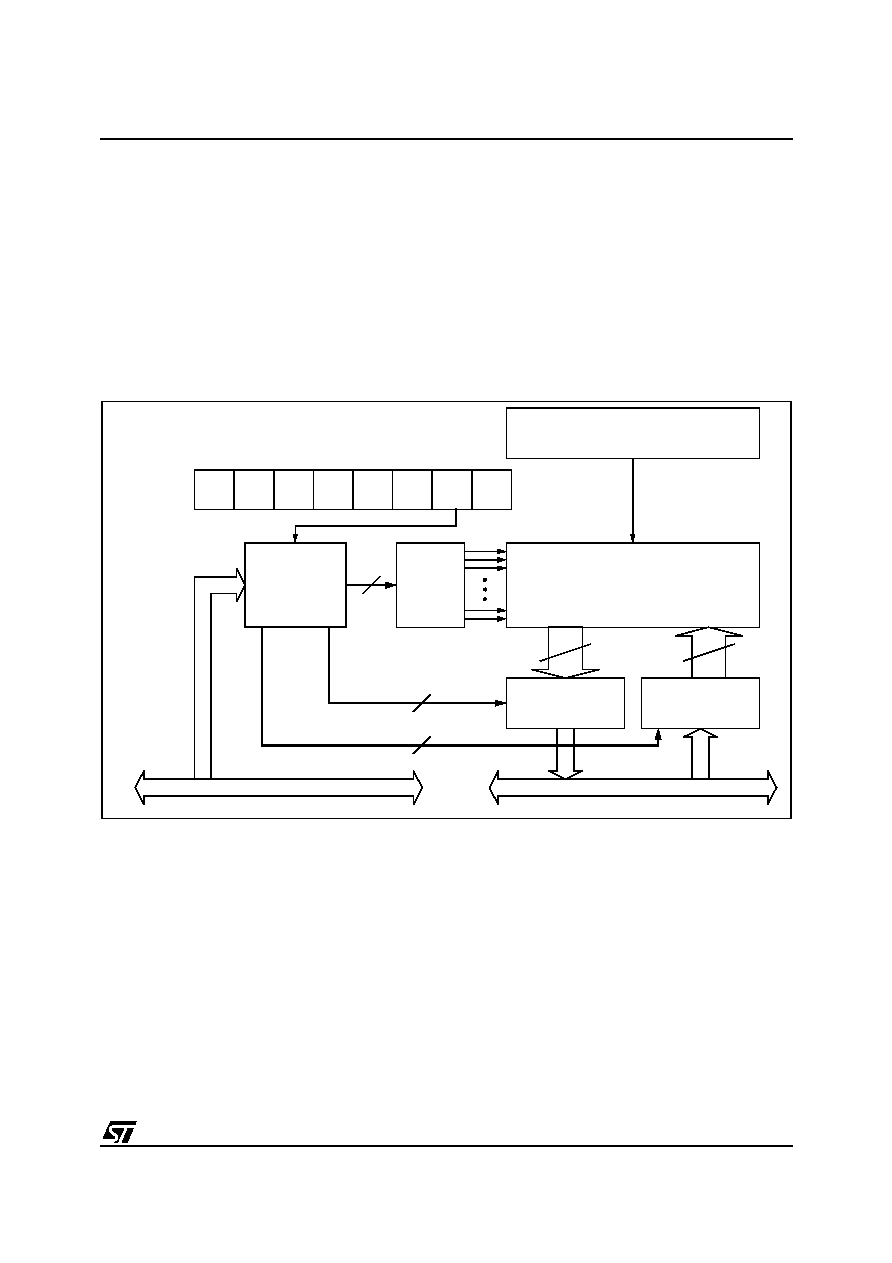
Figure 1. General Block Diagram
8-BIT CORE
ALU
A
DDRE
S
S
A
N
D
DA
T
A
B
U
S
RESET
PORT B
PORT A
SPI
8-BIT ADC
w/ WATCHDOG
PB4:0
(5 bits)
1 MHz. RC OSC
Internal
CLOCK
CONTROL
RAM
(128 Bytes)
PA7:0
(8 bits)
V
SS
V
DD
POWER
SUPPLY
FLASH
(1 or 1.5K Bytes)
LVD/AVD
+
PLL x 4 or x 8
LITE TIMER
MEMORY
DATA EEPROM
(128 Bytes)
12-BIT AUTO-
RELOAD TIMER
1
ST7LITE0, ST7SUPERLITE
6/122
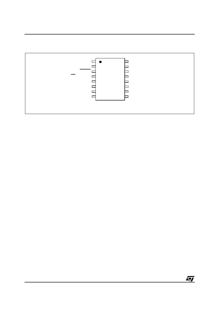
2 PIN DESCRIPTION
Figure 2. 16-Pin Package Pinout (150mil)
16
15
14
13
12
11
10
9
1
2
3
4
5
6
7
8
V
SS
V
DD
SS/AIN0/PB0
CLKIN/AIN4/PB4
MOSI/AIN3/PB3
MISO/AIN2/PB2
SCK/AIN1/PB1
RESET
PA0
(HS)/LTIC
PA1
(HS)
PA7
PA6/MCO/ICCCLK
PA5
(HS)/ICCDATA
PA4
(HS)
PA3
(HS)
PA2
(HS)/ATPWM0
ei1
ei0
(HS) 20mA high sink capability
ei
x
associated external interrupt vector
ei2
ei3
1
ST7LITE0, ST7SUPERLITE
7/122
PIN DESCRIPTION (Cont'd)
Legend / Abbreviations for
Table 1
:
Type:
I = input, O = output, S = supply
In/Output level: C= CMOS 0.15V
DD
/0.85V
DD
with input trigger
C
T
= CMOS 0.3V
DD
/0.7V
DD
with input trigger
Output level:
HS = 20mA high sink (on N-buffer only)
Port and control configuration:
≠ Input:
float = floating, wpu = weak pull-up, int = interrupt
1)
, ana = analog
≠ Output:
OD = open drain
2)
, PP = push-pull
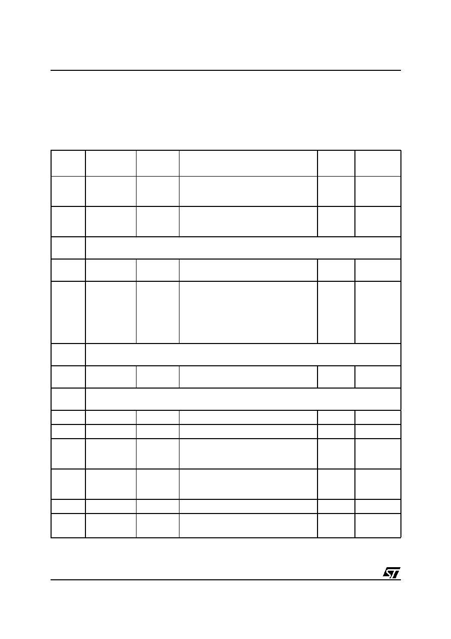
Table 1. Device Pin Description
Note:
In the interrupt input column, "ei
x
" defines the associated external interrupt vector. If the weak pull-up col-
umn (wpu) is merged with the interrupt column (int), then the I/O configuration is pull-up interrupt input,
else the configuration is floating interrupt input.
Pin
n∞
Pin Name
Typ
e
Level
Port / Control
Main
Function
(after reset)
Alternate Function
I
nput
O
utput
Input
Output
flo
at
wp
u
in
t
an
a
OD
PP
1
V
SS
S Ground
2
V
DD
S
Main power supply
3
RESET I/O
C
T
X
X
Top priority non maskable interrupt (active low)
4
PB0/AIN0/SS
I/O C
T
X
ei3
X
X
Port B0
ADC Analog Input 0 or SPI Slave
Select (active low)
5
PB1/AIN1/SCK
I/O C
T
X
X
X
X
Port B1
ADC Analog Input 1 or SPI Clock
6
PB2/AIN2/MISO
I/O C
T
X
X
X
X
Port B2
ADC Analog Input 2 or SPI Master
In/ Slave Out Data
7
PB3/AIN3/MOSI
I/O C
T
X
ei2
X
X
Port B3
ADC Analog Input 3 or SPI Master
Out / Slave In Data
8
PB4/AIN4/CLKIN
I/O C
T
X
X
X
X
Port B4
ADC Analog Input 4 or External
clock input
9
PA7
I/O C
T
X
ei1
X
X
Port A7
10
PA6 /MCO/ICCCLK
I/O
C
T
X
X
X
X
Port A6
Main Clock Output/In Circuit Com-
munication Clock.
Caution: During reset, this pin
must be held at high level to avoid
entering ICC mode unexpectedly
(this is guaranteed by the internal
pull-up if the application leaves the
pin floating).
11
PA5/
ICCDATA
I/O C
T
HS
X
X
X
X
Port A5
In Circuit Communication Data
12
PA4
I/O C
T
HS
X
X
X
X
Port A4
13
PA3
I/O C
T
HS
X
X
X
X
Port A3
14
PA2/ATPWM0
I/O C
T
HS
X
X
X
X
Port A2
Auto-Reload Timer PWM0
15
PA1
I/O C
T
HS
X
X
X
X
Port A1
16
PA0/LTIC
I/O C
T
HS
X
ei0
X
X
Port A0
Lite Timer Input Capture
1

ST7LITE0, ST7SUPERLITE
8/122
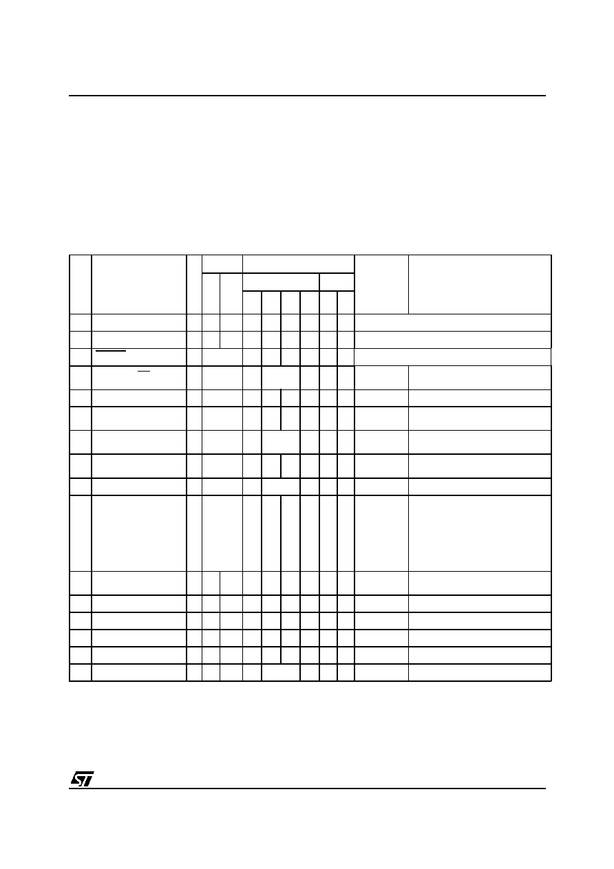
3 REGISTER & MEMORY MAP
As shown in
Figure 3
and
Figure 4
, the MCU is ca-
pable of addressing 64K bytes of memories and I/
O registers.
The available memory locations consist of up to
128 bytes of register locations, 128 bytes of RAM,
128 bytes of data EEPROM and up to 1.5 Kbytes
of user program memory. The RAM space in-
cludes up to 64 bytes for the stack from 0C0h to
0FFh.
The highest address bytes contain the user reset
and interrupt vectors.
The size of Flash Sector 0 is configurable by Op-
tion byte.
IMPORTANT: Memory locations marked as "Re-
served" must never be accessed. Accessing a re-
seved area can have unpredictable effects on the
device.
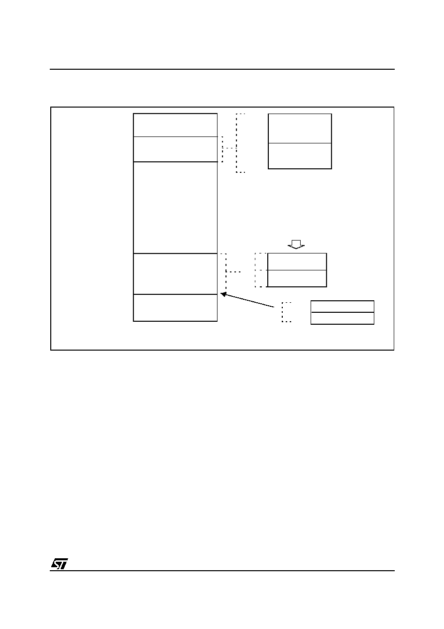
Figure 3. Memory Map (ST7LITE0)
0000h
RAM
Flash Memory
(1.5K)
Interrupt & Reset Vectors
HW Registers
0080h
007Fh
0FFFh
(see
Table 2
)
1000h
107Fh
FFE0h
FFFFh
(see
Table 7
)
0100h
Reserved
00FFh
Short Addressing
RAM (zero page)
64 Bytes Stack
00C0h
00FFh
0080h
00BFh
(128 Bytes)
Data EEPROM
(128 Bytes)
FA00h
1080h
F9FFh
Reserved
FFDFh
1 Kbytes
0.5 Kbytes
SECTOR 1
SECTOR 0
1.5K FLASH
FFFFh
FC00h
FBFFh
FA00h
PROGRAM MEMORY
1000h
1001h
RCCR0
RCCR1
see
section 7.1 on page 23
FFDEh
FFDFh
RCCR0
RCCR1
see
section 7.1 on page 23
1
ST7LITE0, ST7SUPERLITE
9/122
REGISTER AND MEMORY MAP (Cont'd)
Figure 4. Memory Map (ST7SUPERLITE)
0000h
RAM
Flash Memory
(1K)
Interrupt & Reset Vectors
HW Registers
0080h
007Fh
(see
Table 2
)
FFE0h
FFFFh
(see
Table 7
)
0100h
00FFh
Short Addressing
RAM (zero page)
64 Bytes Stack
00C0h
00FFh
0080h
00BFh
(128 Bytes)
FC00h
FBFFh
Reserved
FFDFh
0.5 Kbytes
0.5 Kbytes
SECTOR 1
SECTOR 0
1K FLASH
FFFFh
FE00h
FDFFh
FC00h
PROGRAM MEMORY
FFDEh
FFDFh
RCCR0
RCCR1
see
section 7.1 on page 23
1
ST7LITE0, ST7SUPERLITE
10/122
REGISTER AND MEMORY MAP (Cont'd)
Legend: x=undefined, R/W=read/write
Table 2. Hardware Register Map
Address
Block
Register
Label
Register Name
Reset
Status
Remarks
0000h
0001h
0002h
Port A
PADR
PADDR
PAOR
Port A Data Register
Port A Data Direction Register
Port A Option Register
00h
1)
00h
40h
R/W
R/W
R/W
0003h
0004h
0005h
Port B
PBDR
PBDDR
PBOR
Port B Data Register
Port B Data Direction Register
Port B Option Register
E0h
1)
00h
00h
R/W
R/W
R/W
2)
0006h to
000Ah
Reserved area (5 bytes)
000Bh
000Ch
LITE
TIMER
LTCSR
LTICR
Lite Timer Control/Status Register
Lite Timer Input Capture Register
xxh
xxh
R/W
Read Only
000Dh
000Eh
000Fh
0010h
0011h
0012h
0013h
AUTO-RELOAD
TIMER
ATCSR
CNTRH
CNTRL
ATRH
ATRL
PWMCR
PWM0CSR
Timer Control/Status Register
Counter Register High
Counter Register Low
Auto-Reload Register High
Auto-Reload Register Low
PWM Output Control Register
PWM 0 Control/Status Register
00h
00h
00h
00h
00h
00h
00h
R/W
Read Only
Read Only
R/W
R/W
R/W
R/W
0014h to
0016h
Reserved area (3 bytes)
0017h
0018h
AUTO-RELOAD
TIMER
DCR0H
DCR0L
PWM 0 Duty Cycle Register High
PWM 0 Duty Cycle Register Low
00h
00h
R/W
R/W
0019h to
002Eh
Reserved area (22 bytes)
0002Fh
FLASH
FCSR
Flash Control/Status Register
00h
R/W
00030h
EEPROM
EECSR
Data EEPROM Control/Status Register
00h
R/W
0031h
0032h
0033h
SPI
SPIDR
SPICR
SPICSR
SPI Data I/O Register
SPI Control Register
SPI Control/Status Register
xxh
0xh
00h
R/W
R/W
R/W
0034h
0035h
0036h
ADC
ADCCSR
ADCDAT
ADCAMP
A/D Control Status Register
A/D Data Register
A/D Amplifier Control Register
00h
00h
00h
R/W
Read Only
R/W
0037h
ITC
EICR
External Interrupt Control Register
00h
R/W
0038h
0039h
CLOCKS
MCCSR
RCCR
Main Clock Control/Status Register
RC oscillator Control Register
00h
FFh
R/W
R/W
1

ST7LITE0, ST7SUPERLITE
11/122
Notes:
1. The contents of the I/O port DR registers are readable only in output configuration. In input configura-
tion, the values of the I/O pins are returned instead of the DR register contents.
2. The bits associated with unavailable pins must always keep their reset value.
003Ah
SI
SICSR
System Integrity Control/Status Register
0xh
R/W
003Bh to
007Fh
Reserved area (45 bytes)
Address
Block
Register
Label
Register Name
Reset
Status
Remarks
1

ST7LITE0, ST7SUPERLITE
12/122
4 FLASH PROGRAM MEMORY
4.1 Introduction
The ST7 single voltage extended Flash (XFlash) is
a non-volatile memory that can be electrically
erased and programmed either on a byte-by-byte
basis or up to 32 bytes in parallel.
The XFlash devices can be programmed off-board
(plugged in a programming tool) or on-board using
In-Circuit Programming or In-Application Program-
ming.
The array matrix organisation allows each sector
to be erased and reprogrammed without affecting
other sectors.
4.2 Main Features
s
ICP (In-Circuit Programming)
s
IAP (In-Application Programming)
s
ICT (In-Circuit Testing) for downloading and
executing user application test patterns in RAM
s
Sector 0 size configurable by option byte
s
Read-out and write protection against piracy
4.3 PROGRAMMING MODES
The ST7 can be programmed in three different
ways:
≠ Insertion in a programming tool. In this mode,
FLASH sectors 0 and 1, option byte row and
data EEPROM can be programmed or
erased.
≠ In-Circuit Programming. In this mode, FLASH
sectors 0 and 1, option byte row and data
EEPROM can be programmed or erased with-
out removing the device from the application
board.
≠ In-Application Programming. In this mode,
sector 1 and data EEPROM can be pro-
grammed or erased without removing the de-
vice from the application board and while the
application is running.
4.3.1 In-Circuit Programming (ICP)
ICP uses a protocol called ICC (In-Circuit Commu-
nication) which allows an ST7 plugged on a print-
ed circuit board (PCB) to communicate with an ex-
ternal programming device connected via cable.
ICP is performed in three steps:
Switch the ST7 to ICC mode (In-Circuit Communi-
cations). This is done by driving a specific signal
sequence on the ICCCLK/DATA pins while the
RESET pin is pulled low. When the ST7 enters
ICC mode, it fetches a specific RESET vector
which points to the ST7 System Memory contain-
ing the ICC protocol routine. This routine enables
the ST7 to receive bytes from the ICC interface.
≠ Download ICP Driver code in RAM from the
ICCDATA pin
≠ Execute ICP Driver code in RAM to program
the FLASH memory
Depending on the ICP Driver code downloaded in
RAM, FLASH memory programming can be fully
customized (number of bytes to program, program
locations, or selection of the serial communication
interface for downloading).
4.3.2 In Application Programming (IAP)
This mode uses an IAP Driver program previously
programmed in Sector 0 by the user (in ICP
mode).
This mode is fully controlled by user software. This
allows it to be adapted to the user application, (us-
er-defined strategy for entering programming
mode, choice of communications protocol used to
fetch the data to be stored etc.)
IAP mode can be used to program any memory ar-
eas except Sector 0, which is write/erase protect-
ed to allow recovery in case errors occur during
the programming operation.
1

ST7LITE0, ST7SUPERLITE
13/122
FLASH PROGRAM MEMORY (Cont'd)
4.4 ICC interface
ICP needs a minimum of 4 and up to 6 pins to be
connected to the programming tool. These pins
are:
≠ RESET: device reset
≠ V
SS
: device power supply ground
≠ ICCCLK: ICC output serial clock pin
≠ ICCDATA: ICC input serial data pin
≠ CLKIN: main clock input for external source
≠ V
DD
: application board power supply (option-
al, see Note 3)
Notes:
1. If the ICCCLK or ICCDATA pins are only used
as outputs in the application, no signal isolation is
necessary. As soon as the Programming Tool is
plugged to the board, even if an ICC session is not
in progress, the ICCCLK and ICCDATA pins are
not available for the application. If they are used as
inputs by the application, isolation such as a serial
resistor has to be implemented in case another de-
vice forces the signal. Refer to the Programming
Tool documentation for recommended resistor val-
ues.
2. During the ICP session, the programming tool
must control the RESET pin. This can lead to con-
flicts between the programming tool and the appli-
cation reset circuit if it drives more than 5mA at
high level (push pull output or pull-up resistor<1K).
A schottky diode can be used to isolate the appli-
cation RESET circuit in this case. When using a
classical RC network with R>1K or a reset man-
agement IC with open drain output and pull-up re-
sistor>1K, no additional components are needed.
In all cases the user must ensure that no external
reset is generated by the application during the
ICC session.
3. The use of Pin 7 of the ICC connector depends
on the Programming Tool architecture. This pin
must be connected when using most ST Program-
ming Tools (it is used to monitor the application
power supply). Please refer to the Programming
Tool manual.
4. Pin 9 has to be connected to the CLKIN pin of
the ST7 when the clock is not available in the ap-
plication or if the selected clock option is not pro-
grammed in the option byte.
5. During reset, this pin must be held at high level
to avoid entering ICC mode unexpectedly (this is
guaranteed by the internal pull-up if the application
leaves the pin floating).
Figure 5. Typical ICC Interface
ICC CONNECTOR
I
C
CDA
T
A
I
CCC
L
K
RE
S
E
T
VD
D
HE10 CONNECTOR TYPE
APPLICATION
POWER SUPPLY
1
2
4
6
8
10
9
7
5
3
PROGRAMMING TOOL
ICC CONNECTOR
APPLICATION BOARD
ICC Cable
OPTIONAL
(See Note 3)
ST7
CL
K
I
N
OPTIONAL
See Note 1
See Notes 1 and 5
See Note 2
APPLICATION
RESET SOURCE
APPLICATION
I/O
(See Note 4)
1
ST7LITE0, ST7SUPERLITE
14/122
FLASH PROGRAM MEMORY (Cont'd)
4.5 Memory Protection
There are two different types of memory protec-
tion: Read Out Protection and Write/Erase Protec-
tion which can be applied individually.
4.5.1 Read out Protection
Read out protection, when selected, makes it im-
possible to extract the memory content from the
microcontroller, thus preventing piracy. Both pro-
gram and data E
2
memory are protected.
In flash devices, this protection is removed by re-
programming the option. In this case, both pro-
gram and data E
2
memory are automatically
erased, and the device can be reprogrammed.
Read-out protection selection depends on the de-
vice type:
≠ In Flash devices it is enabled and removed
through the FMP_R bit in the option byte.
≠ In ROM devices it is enabled by mask option
specified in the Option List.
4.5.2 Flash Write/Erase Protection
Write/erase protection, when set, makes it impos-
sible to both overwrite and erase program memo-
ry. It does not apply to E
2
data. Its purpose is to
provide advanced security to applications and pre-
vent any change being made to the memory con-
tent.
Warning: Once set, Write/erase protection can
never be removed. A write-protected flash device
is no longer reprogrammable.
Write/erase protection is enabled through the
FMP_W bit in the option byte.
4.6 Related Documentation
For details on Flash programming and ICC proto-
col, refer to the ST7 Flash Programming Refer-
ence Manual and to the ST7 ICC Protocol Refer-
ence Manual
.
4.7 Register Description
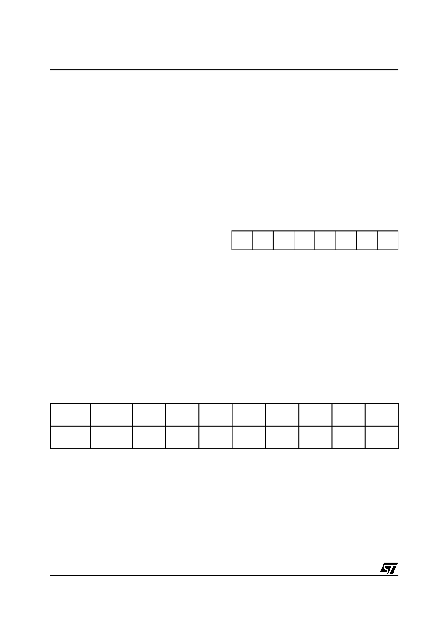
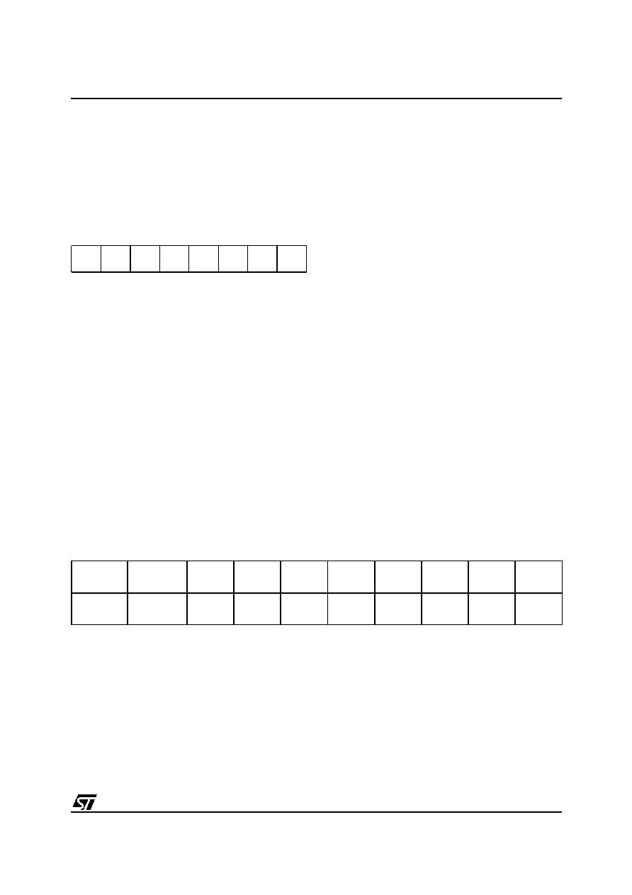
FLASH CONTROL/STATUS REGISTER (FCSR)
Read /Write
Reset Value: 000 0000 (00h)
1st RASS Key: 0101 0110 (56h)
2nd RASS Key: 1010 1110 (AEh)
Note: This register is reserved for programming
using ICP, IAP or other programming methods. It
controls the XFlash programming and erasing op-
erations.
When an EPB or another programming tool is
used (in socket or ICP mode), the RASS keys are
sent automatically.
Table 3. FLASH Register Map and Reset Values
7
0
0
0
0
0
0
OPT
LAT
PGM
Address
(Hex.)
Register
Label
7
6
5
4
3
2
1
0
002Fh
FCSR
Reset Value
0
0
0
0
0
OPT
0
LAT
0
PGM
0
1
ST7LITE0, ST7SUPERLITE
15/122
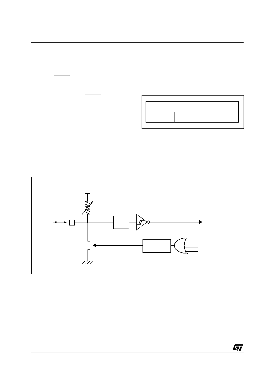
5 DATA EEPROM
5.1 INTRODUCTION
The Electrically Erasable Programmable Read
Only Memory can be used as a non volatile back-
up for storing data. Using the EEPROM requires a
basic access protocol described in this chapter.
5.2 MAIN FEATURES
s
Up to 32 Bytes programmed in the same cycle
s
EEPROM mono-voltage (charge pump)
s
Chained erase and programming cycles
s
Internal control of the global programming cycle
duration
s
WAIT mode management
s
Readout protection against piracy
Figure 6. EEPROM Block Diagram
EECSR
HIGH VOLTAGE
PUMP
0
E2LAT
0
0
0
0
0
E2PGM
EEPROM
MEMORY MATRIX
(1 ROW = 32 x 8 BITS)
ADDRESS
DECODER
DATA
MULTIPLEXER
32 x 8 BITS
DATA LATCHES
ROW
DECODER
DATA BUS
4
4
4
128
128
ADDRESS BUS
1
ST7LITE0, ST7SUPERLITE
16/122
DATA EEPROM (Cont'd)
5.3 MEMORY ACCESS
The Data EEPROM memory read/write access
modes are controlled by the E2LAT bit of the EEP-
ROM Control/Status register (EECSR). The flow-
chart in
Figure 7
describes these different memory
access modes.
Read Operation (E2LAT=0)
The EEPROM can be read as a normal ROM loca-
tion when the E2LAT bit of the EECSR register is
cleared. In a read cycle, the byte to be accessed is
put on the data bus in less than 1 CPU clock cycle.
This means that reading data from EEPROM
takes the same time as reading data from
EPROM, but this memory cannot be used to exe-
cute machine code.
Write Operation (E2LAT=1)
To access the write mode, the E2LAT bit has to be
set by software (the E2PGM bit remains cleared).
When a write access to the EEPROM area occurs,
the value is latched inside the 32 data latches ac-
cording to its address.
When PGM bit is set by the software, all the previ-
ous bytes written in the data latches (up to 32) are
programmed in the EEPROM cells. The effective
high address (row) is determined by the last EEP-
ROM write sequence. To avoid wrong program-
ming, the user must take care that all the bytes
written between two programming sequences
have the same high address: only the five Least
Significant Bits of the address can change.
At the end of the programming cycle, the PGM and
LAT bits are cleared simultaneously.
Note: Care should be taken during the program-
ming cycle. Writing to the same memory location
will over-program the memory (logical AND be-
tween the two write access data result) because
the data latches are only cleared at the end of the
programming cycle and by the falling edge of the
E2LAT bit.
It is not possible to read the latched data.
This note is ilustrated by the
Figure 9
.
Figure 7. Data EEPROM Programming Flowchart
READ MODE
E2LAT=0
E2PGM=0
WRITE MODE
E2LAT=1
E2PGM=0
READ BYTES
IN EEPROM AREA
WRITE UP TO 32 BYTES
IN EEPROM AREA
(with the same 11 MSB of the address)
START PROGRAMMING CYCLE
E2LAT=1
E2PGM=1 (set by software)
E2LAT
0
1
CLEARED BY HARDWARE
1

ST7LITE0, ST7SUPERLITE
17/122
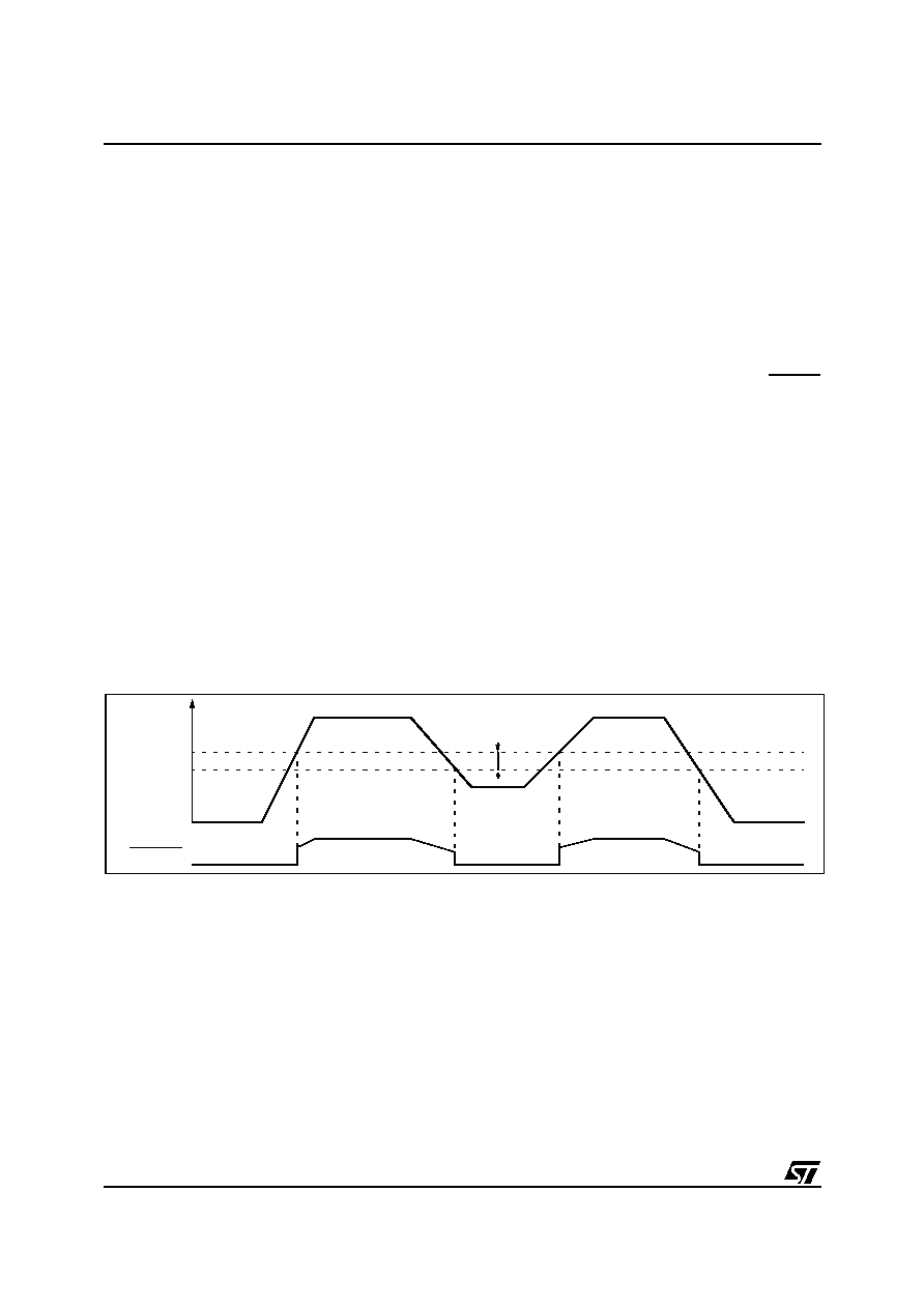
DATA EEPROM (Cont'd)
Figure 8. Data E
2
PROM Write Operation
Note: If a programming cycle is interrupted (by software or a reset action), the integrity of the data in mem-
ory is not guaranteed.
Byte 1
Byte 2
Byte 32
PHASE 1
Programming cycle
Read operation impossible
PHASE 2
Read operation possible
E2LAT bit
E2PGM bit
Writing data latches
Waiting E2PGM and E2LAT to fall
Set by USER application
Cleared by hardware
Row / Byte
0
1
2
3
...
30 31
Physical Address
0
00h...1Fh
1
20h...3Fh
...
N
Nx20h...Nx20h+1Fh
ROW
DEFINITION
1
ST7LITE0, ST7SUPERLITE
18/122
DATA EEPROM (Cont'd)
5.4 POWER SAVING MODES
Wait mode
The DATA EEPROM can enter WAIT mode on ex-
ecution of the WFI instruction of the microcontrol-
ler or when the microcontroller enters Active-HALT
mode.The DATA EEPROM will immediately enter
this mode if there is no programming in progress,
otherwise the DATA EEPROM will finish the cycle
and then enter WAIT mode.
Active-Halt mode
Refer to Wait mode.
Halt mode
The DATA EEPROM immediately enters HALT
mode if the microcontroller executes the HALT in-
struction. Therefore the EEPROM will stop the
function in progress, and data may be corrupted.
5.5 ACCESS ERROR HANDLING
If a read access occurs while E2LAT=1, then the
data bus will not be driven.
If a write access occurs while E2LAT=0, then the
data on the bus will not be latched.
If a programming cycle is interrupted (by software/
RESET action), the memory data will not be guar-
anteed.
5.6 Data EEPROM Read-out Protection
The read-out protection is enabled through an op-
tion bit (see
section 15.1 on page 109
).
When this option is selected, the programs and
data stored in the EEPROM memory are protected
against read-out piracy (including a re-write pro-
tection). In Flash devices, when this protection is
removed by reprogramming the Option Byte, the
entire Program memeory and EEPROM is first au-
tomatically erased.
Note: Both Program Memory and data EEPROM
are protected using the same option bit.
Figure 9. Data EEPROM Programming Cycle
LAT
ERASE CYCLE
WRITE CYCLE
PGM
t
PROG
READ OPERATION NOT POSSIBLE
WRITE OF
DATA LATCHES
READ OPERATION POSSIBLE
INTERNAL
PROGRAMMING
VOLTAGE
1
ST7LITE0, ST7SUPERLITE
19/122
DATA EEPROM (Cont'd)
5.7 REGISTER DESCRIPTION
EEPROM CONTROL/STATUS REGISTER (EEC-
SR)
Read /Write
Reset Value: 0000 0000 (00h)
Bits 7:2 = Reserved, forced by hardware to 0.
Bit 1 = E2LAT
Latch Access Transfer
This bit is set by software. It is cleared by hard-
ware at the end of the programming cycle. It can
only be cleared by software if the E2PGM bit is
cleared.
0: Read mode
1: Write mode
Bit 0 = E2PGM
Programming control and status
This bit is set by software to begin the programming
cycle. At the end of the programming cycle, this bit
is cleared by hardware.
0: Programming finished or not yet started
1: Programming cycle is in progress
Note: if the E2PGM bit is cleared during the pro-
gramming cycle, the memory data is not guaran-
teed
Table 4. DATA EEPROM Register Map and Reset Values
7
0
0
0
0
0
0
0
E2LAT E2PGM
Address
(Hex.)
Register
Label
7
6
5
4
3
2
1
0
0030h
EECSR
Reset Value
0
0
0
0
0
0
E2LAT
0
E2PGM
0
1
ST7LITE0, ST7SUPERLITE
20/122
6 CENTRAL PROCESSING UNIT
6.1 INTRODUCTION
This CPU has a full 8-bit architecture and contains
six internal registers allowing efficient 8-bit data
manipulation.
6.2 MAIN FEATURES
s
63 basic instructions
s
Fast 8-bit by 8-bit multiply
s
17 main addressing modes
s
Two 8-bit index registers
s
16-bit stack pointer
s
Low power modes
s
Maskable hardware interrupts
s
Non-maskable software interrupt
6.3 CPU REGISTERS
The 6 CPU registers shown in
Figure 10
are not
present in the memory mapping and are accessed
by specific instructions.
Accumulator (A)
The Accumulator is an 8-bit general purpose reg-
ister used to hold operands and the results of the
arithmetic and logic calculations and to manipulate
data.
Index Registers (X and Y)
In indexed addressing modes, these 8-bit registers
are used to create either effective addresses or
temporary storage areas for data manipulation.
(The Cross-Assembler generates a precede in-
struction (PRE) to indicate that the following in-
struction refers to the Y register.)
The Y register is not affected by the interrupt auto-
matic procedures (not pushed to and popped from
the stack).
Program Counter (PC)
The program counter is a 16-bit register containing
the address of the next instruction to be executed
by the CPU. It is made of two 8-bit registers PCL
(Program Counter Low which is the LSB) and PCH
(Program Counter High which is the MSB).
Figure 10. CPU Registers
ACCUMULATOR
X INDEX REGISTER
Y INDEX REGISTER
STACK POINTER
CONDITION CODE REGISTER
PROGRAM COUNTER
7
0
1
C
1 1 H I
N Z
RESET VALUE = RESET VECTOR @ FFFEh-FFFFh
7
0
7
0
7
0
0
7
15
8
PCH
PCL
15
8
7
0
RESET VALUE = STACK HIGHER ADDRESS
RESET VALUE = 1
X
1 1 X 1 X X
RESET VALUE = XXh
RESET VALUE = XXh
RESET VALUE = XXh
X = Undefined Value
1

ST7LITE0, ST7SUPERLITE
21/122
CPU REGISTERS (Cont'd)
CONDITION CODE REGISTER (CC)
Read/Write
Reset Value: 111x1xxx
The 8-bit Condition Code register contains the in-
terrupt mask and four flags representative of the
result of the instruction just executed. This register
can also be handled by the PUSH and POP in-
structions.
These bits can be individually tested and/or con-
trolled by specific instructions.
Bit 4 = H
Half carry
.
This bit is set by hardware when a carry occurs be-
tween bits 3 and 4 of the ALU during an ADD or
ADC instruction. It is reset by hardware during the
same instructions.
0: No half carry has occurred.
1: A half carry has occurred.
This bit is tested using the JRH or JRNH instruc-
tion. The H bit is useful in BCD arithmetic subrou-
tines.
Bit 3 = I
Interrupt mask
.
This bit is set by hardware when entering in inter-
rupt or by software to disable all interrupts except
the TRAP software interrupt. This bit is cleared by
software.
0: Interrupts are enabled.
1: Interrupts are disabled.
This bit is controlled by the RIM, SIM and IRET in-
structions and is tested by the JRM and JRNM in-
structions.
Note: Interrupts requested while I is set are
latched and can be processed when I is cleared.
By default an interrupt routine is not interruptable
because the I bit is set by hardware at the start of
the routine and reset by the IRET instruction at the
end of the routine. If the I bit is cleared by software
in the interrupt routine, pending interrupts are
serviced regardless of the priority level of the cur-
rent interrupt routine.
Bit 2 = N
Negative
.
This bit is set and cleared by hardware. It is repre-
sentative of the result sign of the last arithmetic,
logical or data manipulation. It is a copy of the 7
th
bit of the result.
0: The result of the last operation is positive or null.
1: The result of the last operation is negative
(i.e. the most significant bit is a logic 1).
This bit is accessed by the JRMI and JRPL instruc-
tions.
Bit 1 = Z
Zero
.
This bit is set and cleared by hardware. This bit in-
dicates that the result of the last arithmetic, logical
or data manipulation is zero.
0: The result of the last operation is different from
zero.
1: The result of the last operation is zero.
This bit is accessed by the JREQ and JRNE test
instructions.
Bit 0 = C
Carry/borrow.
This bit is set and cleared by hardware and soft-
ware. It indicates an overflow or an underflow has
occurred during the last arithmetic operation.
0: No overflow or underflow has occurred.
1: An overflow or underflow has occurred.
This bit is driven by the SCF and RCF instructions
and tested by the JRC and JRNC instructions. It is
also affected by the "bit test and branch", shift and
rotate instructions.
7
0
1
1
1
H
I
N
Z
C
1
ST7LITE0, ST7SUPERLITE
22/122
CPU REGISTERS (Cont'd)
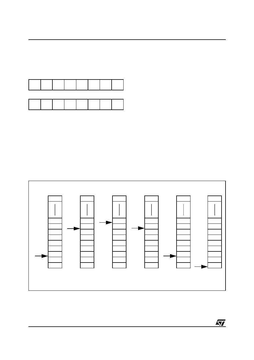
Stack Pointer (SP)
Read/Write
Reset Value: 00 FFh
The Stack Pointer is a 16-bit register which is al-
ways pointing to the next free location in the stack.
It is then decremented after data has been pushed
onto the stack and incremented before data is
popped from the stack (see
Figure 11
).
Since the stack is 64 bytes deep, the 10 most sig-
nificant bits are forced by hardware. Following an
MCU Reset, or after a Reset Stack Pointer instruc-
tion (RSP), the Stack Pointer contains its reset val-
ue (the SP5 to SP0 bits are set) which is the stack
higher address.
The least significant byte of the Stack Pointer
(called S) can be directly accessed by a LD in-
struction.
Note: When the lower limit is exceeded, the Stack
Pointer wraps around to the stack upper limit, with-
out indicating the stack overflow. The previously
stored information is then overwritten and there-
fore lost. The stack also wraps in case of an under-
flow.
The stack is used to save the return address dur-
ing a subroutine call and the CPU context during
an interrupt. The user may also directly manipulate
the stack by means of the PUSH and POP instruc-
tions. In the case of an interrupt, the PCL is stored
at the first location pointed to by the SP. Then the
other registers are stored in the next locations as
shown in
Figure 11
.
≠ When an interrupt is received, the SP is decre-
mented and the context is pushed on the stack.
≠ On return from interrupt, the SP is incremented
and the context is popped from the stack.
A subroutine call occupies two locations and an in-
terrupt five locations in the stack area.
Figure 11. Stack Manipulation Example
15
8
0
0
0
0
0
0
0
0
7
0
1
1
SP5
SP4
SP3
SP2
SP1
SP0
PCH
PCL
SP
PCH
PCL
SP
PCL
PCH
X
A
CC
PCH
PCL
SP
PCL
PCH
X
A
CC
PCH
PCL
SP
PCL
PCH
X
A
CC
PCH
PCL
SP
SP
Y
CALL
Subroutine
Interrupt
event
PUSH Y
POP Y
IRET
RET
or RSP
@ 00FFh
@ 00C0h
Stack Higher Address = 00FFh
Stack Lower Address = 00C0h
1

ST7LITE0, ST7SUPERLITE
23/122
7 SUPPLY, RESET AND CLOCK MANAGEMENT
The device includes a range of utility features for
securing the application in critical situations (for
example in case of a power brown-out), and re-
ducing the number of external components.
Main features
s
Clock Management
≠ 1 MHz internal RC oscillator (enabled by op-
tion byte)
≠ External Clock Input (enabled by option byte)
≠ PLL for multiplying the frequency by 4 or 8
(enabled by option byte)
s
Reset Sequence Manager (RSM)
s
System Integrity Management (SI)
≠ Main supply Low voltage detection (LVD) with
reset generation (enabled by option byte)
≠ Auxiliary Voltage detector (AVD) with interrupt
capability for monitoring the main supply (en-
abled by option byte)
7.1 INTERNAL RC OSCILLATOR ADJUSTMENT
The ST7LITE0 and ST7SUPERLITE contain an in-
ternal RC oscillator with an accuracy of 1% for a
given device, temperature and voltage. It must be
calibrated to obtain the frequency required in the
application. This is done by software writing a cal-
ibration value in the RCCR (RC Control Register).
Whenever the microcontroller is reset, the RCCR
returns to its default value (FFh), i.e. each time the
device is reset, the calibration value must be load-
ed in the RCCR. Predefined calibration values are
stored in EEPROM for 3.0 and 5V V
DD
supply volt-
ages at 25∞C, as shown in the following table.
Notes:
≠ See "ELECTRICAL CHARACTERISTICS" on
page 78. for more information on the frequency
and accuracy of the RC oscillator.
≠ To improve clock stability, it is recommended to
place a decoupling capacitor between the V
DD
and V
SS
pins as close as possible to the ST7 de-
vice.
≠ These two bytes are systematically programmed
by ST, including on FASTROM devices. Conse-
quently, customers intending to use FASTROM
service must not use these two bytes.
Caution: If the voltage or temperature conditions
change in the application, the frequency may need
to be recalibrated.
Refer to application note AN1324 for information
on how to calibrate the RC frequency using an ex-
ternal reference signal.
7.2 PHASE LOCKED LOOP
The PLL can be used to multiply a 1MHz frequen-
cy from the RC oscillator or the external clock by 4
or 8 to obtain f
OSC
of 4 or 8 MHz. The PLL is ena-
bled and the multiplication factor of 4 or 8 is select-
ed by 2 option bits.
≠ The x4 PLL is intended for operation with V
DD
in
the 2.4V to 3.3V range
≠ The x8 PLL is intended for operation with V
DD
in
the 3.3V to 5.5V range
Refer to
Section 15.1
for the option byte descrip-
tion.
If the PLL is disabled and the RC oscillator is ena-
bled, then f
OSC =
1MHz.
If both the RC oscillator and the PLL are disabled,
f
OSC
is driven by the external clock.
RCCR
Conditions
ST7FLITE09
Address
ST7FLITE02/
ST7FLITE05/
ST7FLITES2/
ST7FLITES5
Address
RCCR0
V
DD
=5V
T
A
=25∞C
f
RC
=1MHz
1000h and
FFDEh
FFDEh
RCCR1
V
DD
=3.0V
T
A
=25∞C
f
RC
=700KHz
1001h and-
FFDFh
FFDFh
1
ST7LITE0, ST7SUPERLITE
24/122
Figure 12. PLL Output Frequency Timing
Diagram
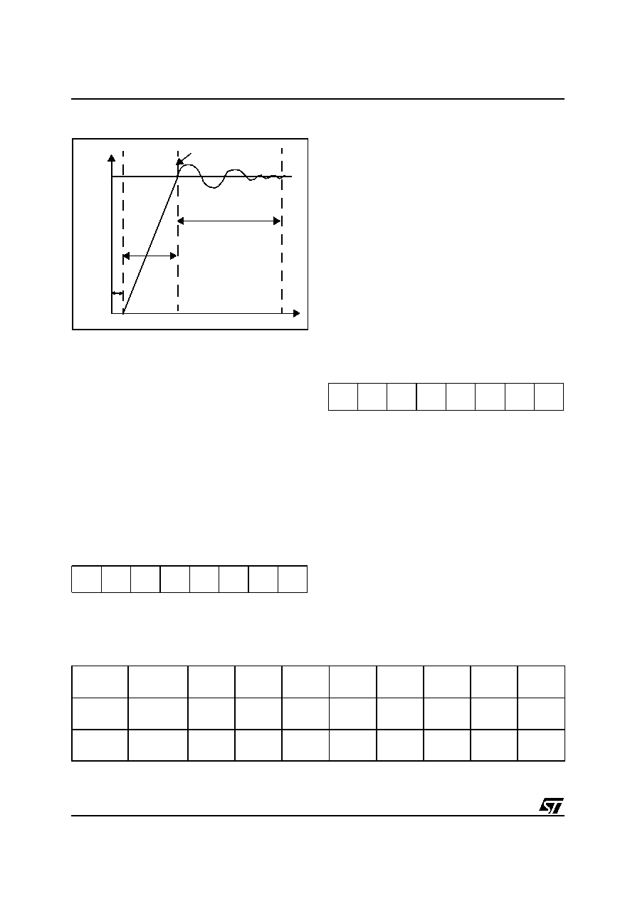
When the PLL is started, after reset or wakeup
from Halt mode or AWUFH mode, it outputs the
clock after a delay of t
STARTUP
.
When the PLL output signal reaches the operating
frequency, the LOCKED bit in the SICSCR register
is set. Full PLL accuracy (ACC
PLL
) is reached after
a stabilization time of t
STAB
(see
Figure 12
and
13.3.4 Internal RC Oscillator and PLL
)
Refer to
section 7.5.4 on page 32
for a description
of the LOCKED bit in the SICSR register.
7.3 REGISTER DESCRIPTION
MAIN CLOCK CONTROL/STATUS REGISTER
(MCCSR)
Read / Write
Reset Value: 0000 0000 (00h)
Bits 7:2 = Reserved, must be kept cleared.
Bit 1 = MCO
Main Clock Out enable
This bit is read/write by software and cleared by
hardware after a reset. This bit allows to enable
the MCO output clock.
0: MCO clock disabled, I/O port free for general
purpose I/O.
1: MCO clock enabled.
Bit 0 = SMS
Slow Mode select
This bit is read/write by software and cleared by
hardware after a reset. This bit selects the input
clock f
OSC
or f
OSC
/32.
0: Normal mode (f
CPU =
f
OSC
1: Slow mode (f
CPU =
f
OSC
/32)
RC CONTROL REGISTER (RCCR)
Read / Write
Reset Value: 1111 1111 (FFh)
Bits 7:0 = CR[7:0]
RC Oscillator Frequency Ad-
justment Bits
These bits must be written immediately after reset
to adjust the RC oscillator frequency and to obtain
an accuracy of 1%. The application can store the
correct value for each voltage range in EEPROM
and write it to this register at start-up.
00h = maximum available frequency
FFh = lowest available frequency
Note: To tune the oscillator, write a series of differ-
ent values in the register until the correct frequen-
cy is reached. The fastest method is to use a di-
chotomy starting with 80h.
Table 5. Clock Register Map and Reset Values
7
0
00
0
0
0
0
0
MCO
SMS
4/8 x
freq.
LOCKED bit set
t
STAB
t
LOCK
input
O
u
tp
u
t
fr
e
q
.
t
STARTUP
t
7
0
CR70 CR60 CR50 CR40 CR30 CR20 CR10
CR
0
Address
(Hex.)
Register
Label
7
6
5
4
3
2
1
0
0038h
MCCSR
Reset Value
0
0
0
0
0
0
MCO
0
SMS
0
0039h
RCCR
Reset Value
CR70
1
CR60
1
CR50
1
CR40
1
CR30
1
CR20
1
CR10
1
CR0
1
1

ST7LITE0, ST7SUPERLITE
25/122
Figure 13. Clock Management Block Diagram
CR4
CR7
CR0
CR1
CR2
CR3
CR6
CR5
RCCR
Tunable
PLL 1MHz -> 8MHz
CLKIN
Option byte
PLL 1MHz -> 4MHz
f
OSC
8MHz
4MHz
1MHz
0 to 8 MHz
MCCSR
SMS
MCO
MCO
f
CPU
f
CPU
TO CPU AND
PERIPHERALS
(1ms timebase @ 8 MHz f
OSC
)
/32 DIVIDER
f
OSC
f
OSC
/32
f
OSC
Oscillator
1% RC
f
LTIMER
1
0
Option byte
LITE TIMER COUNTER
8-BIT
/2 DIVIDER
7
0
(except LITE
TIMER)
1
ST7LITE0, ST7SUPERLITE
26/122
7.4 RESET SEQUENCE MANAGER (RSM)
7.4.1 Introduction
The reset sequence manager includes three RE-
SET sources as shown in
Figure 15
:
s
External RESET source pulse
s
Internal LVD RESET (Low Voltage Detection)
s
Internal WATCHDOG RESET
These sources act on the RESET pin and it is al-
ways kept low during the delay phase.
The RESET service routine vector is fixed at ad-
dresses FFFEh-FFFFh in the ST7 memory map.
The basic RESET sequence consists of 3 phases
as shown in
Figure 14
:
s
Active Phase depending on the RESET source
s
256 CPU clock cycle delay
s
RESET vector fetch
The 256 CPU clock cycle delay allows the oscilla-
tor to stabilise and ensures that recovery has tak-
en place from the Reset state.
The RESET vector fetch phase duration is 2 clock
cycles.
If the PLL is enabled by option byte, it outputs the
clock after an additional delay of t
STARTUP
(see
Figure 12
).
Figure 14. RESET Sequence Phases
Figure 15. Reset Block Diagram
RESET
Active Phase
INTERNAL RESET
256 CLOCK CYCLES
FETCH
VECTOR
RESET
R
ON
V
DD
WATCHDOG RESET
LVD RESET
INTERNAL
RESET
PULSE
GENERATOR
FILTER
1

ST7LITE0, ST7SUPERLITE
27/122
RESET SEQUENCE MANAGER (Cont'd)
7.4.2 Asynchronous External RESET pin
The RESET pin is both an input and an open-drain
output with integrated R
ON
weak pull-up resistor.
This pull-up has no fixed value but varies in ac-
cordance with the input voltage. It
can be pulled
low by external circuitry to reset the device. See
Electrical Characteristic section for more details.
A RESET signal originating from an external
source must have a duration of at least t
h(RSTL)in
in
order to be recognized (see
Figure 16
). This de-
tection is asynchronous and therefore the MCU
can enter reset state even in HALT mode.
The RESET pin is an asynchronous signal which
plays a major role in EMS performance. In a noisy
environment, it is recommended to follow the
guidelines mentioned in the electrical characteris-
tics section.
7.4.3 External Power-On RESET
If the LVD is disabled by option byte, to start up the
microcontroller correctly, the user must ensure by
means of an external reset circuit that the reset
signal is held low until V
DD
is over the minimum
level specified for the selected f
OSC
frequency.
A proper reset signal for a slow rising V
DD
supply
can generally be provided by an external RC net-
work connected to the RESET pin.
7.4.4 Internal Low Voltage Detector (LVD)
RESET
Two different RESET sequences caused by the in-
ternal LVD circuitry can be distinguished:
s
Power-On RESET
s
Voltage Drop RESET
The device RESET pin acts as an output that is
pulled low when V
DD
<V
IT+
(rising edge) or
V
DD
<V
IT-
(falling edge) as shown in
Figure 16
.
The LVD filters spikes on V
DD
larger than t
g(VDD)
to
avoid parasitic resets.
7.4.5 Internal Watchdog RESET
The RESET sequence generated by a internal
Watchdog counter overflow is shown in
Figure 16
.
Starting from the Watchdog counter underflow, the
device RESET pin acts as an output that is pulled
low during at least t
w(RSTL)out
.
Figure 16. RESET Sequences
V
DD
RUN
RESET PIN
EXTERNAL
WATCHDOG
ACTIVE PHASE
V
IT+(LVD)
V
IT-(LVD)
t
h(RSTL)in
RUN
WATCHDOG UNDERFLOW
t
w(RSTL)out
RUN
RUN
RESET
RESET
SOURCE
EXTERNAL
RESET
LVD
RESET
WATCHDOG
RESET
INTERNAL RESET (256 T
CPU
)
VECTOR FETCH
ACTIVE
PHASE
ACTIVE
PHASE
1
ST7LITE0, ST7SUPERLITE
28/122
7.5 SYSTEM INTEGRITY MANAGEMENT (SI)
The System Integrity Management block contains
the Low voltage Detector (LVD) and Auxiliary Volt-
age Detector (AVD) functions. It is managed by
the SICSR register.
7.5.1 Low Voltage Detector (LVD)
The Low Voltage Detector function (LVD) gener-
ates a static reset when the V
DD
supply voltage is
below a V
IT-(LVD)
reference value. This means that
it secures the power-up as well as the power-down
keeping the ST7 in reset.
The V
IT-(LVD)
reference value for a voltage drop is
lower than the V
IT+(LVD)
reference value for power-
on in order to avoid a parasitic reset when the
MCU starts running and sinks current on the sup-
ply (hysteresis).
The LVD Reset circuitry generates a reset when
V
DD
is below:
≠ V
IT+(LVD)
when V
DD
is rising
≠ V
IT-(LVD)
when V
DD
is falling
The LVD function is illustrated in
Figure 17
.
The voltage threshold can be configured by option
byte to be low, medium or high. See
section 15.1
on page 109
.
Provided the minimum V
DD
value (guaranteed for
the oscillator frequency) is above V
IT-(LVD)
, the
MCU can only be in two modes:
≠ under full software control
≠ in static safe reset
In these conditions, secure operation is always en-
sured for the application without the need for ex-
ternal reset hardware.
During a Low Voltage Detector Reset, the RESET
pin is held low, thus permitting the MCU to reset
other devices.
Notes:
The LVD is an optional function which can be se-
lected by option byte. See
section 15.1 on page
109
.
It allows the device to be used without any external
RESET circuitry.
If the LVD is disabled, an external circuitry must be
used to ensure a proper power-on reset.
Caution: If an LVD reset occurs after a watchdog
reset has occurred, the LVD will take priority and
will clear the watchdog flag.
Figure 17. Low Voltage Detector vs Reset
V
DD
V
IT+
(LVD)
RESET
V
IT-
(LVD)
V
hys
1
ST7LITE0, ST7SUPERLITE
29/122
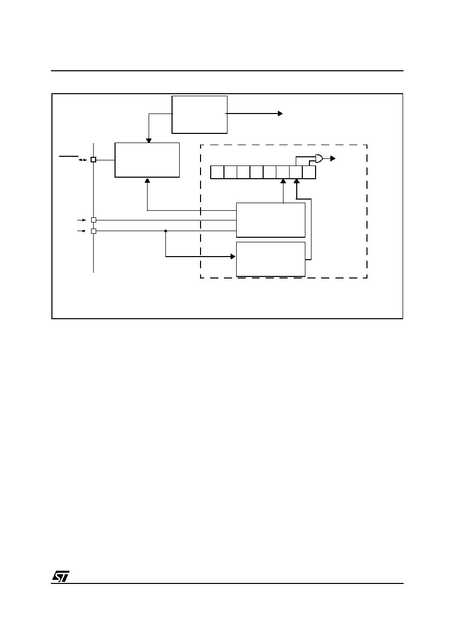
Figure 18. Reset and Supply Management Block Diagram
LOW VOLTAGE
DETECTOR
(LVD)
AUXILIARY VOLTAGE
DETECTOR
(AVD)
RESET
V
SS
V
DD
RESET SEQUENCE
MANAGER
(RSM)
AVD Interrupt Request
SYSTEM INTEGRITY MANAGEMENT
WATCHDOG
SICSR
TIMER (WDG)
AVD
AVD
LVD
RF
IE
0
F
0
STATUS FLAG
0
0
LOC
KED
7
0
1
ST7LITE0, ST7SUPERLITE
30/122
SYSTEM INTEGRITY MANAGEMENT (Cont'd)
7.5.2 Auxiliary Voltage Detector (AVD)
The Voltage Detector function (AVD) is based on
an analog comparison between a V
IT-(AVD)
and
V
IT+(AVD)
reference value and the V
DD
main sup-
ply voltage (V
AVD
). The V
IT-(AVD)
reference value
for falling voltage is lower than the V
IT+(AVD)
refer-
ence value for rising voltage in order to avoid par-
asitic detection (hysteresis).
The output of the AVD comparator is directly read-
able by the application software through a real
time status bit (AVDF) in the SICSR register. This
bit is read only.
Caution: The AVD functions only if the LVD is en-
abled through the option byte.
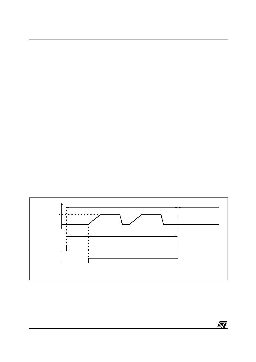
7.5.2.1 Monitoring the V
DD
Main Supply
The AVD voltage threshold value is relative to the
selected LVD threshold configured by option byte
(see
section 15.1 on page 109
).
If the AVD interrupt is enabled, an interrupt is gen-
erated when the voltage crosses the V
IT+(LVD)
or
V
IT-(AVD)
threshold (AVDF bit is set).
In the case of a drop in voltage, the AVD interrupt
acts as an early warning, allowing software to shut
down safely before the LVD resets the microcon-
troller. See
Figure 19
.
The interrupt on the rising edge is used to inform
the application that the V
DD
warning state is over
Figure 19. Using the AVD to Monitor V
DD
V
DD
V
IT+(AVD)
V
IT-(AVD)
AVDF bit
0
1
RESET
IF AVDIE bit = 1
V
hyst
AVD INTERRUPT
REQUEST
INTERRUPT Cleared by
V
IT+(LVD)
V
IT-(LVD)
LVD RESET
Early Warning Interrupt
(Power has dropped, MCU not
not yet in reset)
0
1
hardware
INTERRUPT Cleared by
reset
1

ST7LITE0, ST7SUPERLITE
31/122
SYSTEM INTEGRITY MANAGEMENT (Cont'd)
7.5.3 Low Power Modes
7.5.3.1 Interrupts
The AVD interrupt event generates an interrupt if
the corresponding Enable Control Bit (AVDIE) is
set and the interrupt mask in the CC register is re-
set (RIM instruction).
Mode Description
WAIT
No effect on SI. AVD interrupts cause the
device to exit from Wait mode.
HALT
The CRSR register is frozen.
The AVD remains active but the AVD inter-
rupt cannot be used to exit from Halt mode.
Interrupt Event
Event
Flag
Enable
Control
Bit
Exit
from
Wait
Exit
from
Halt
AVD event
AVDF
AVDIE
Yes
Yes
1

ST7LITE0, ST7SUPERLITE
32/122
SYSTEM INTEGRITY MANAGEMENT (Cont'd)
7.5.4 Register Description
SYSTEM INTEGRITY (SI) CONTROL/STATUS REGISTER (SICSR)
Read /Write
Reset Value: 0000 0x00 (0xh)
Bit 7:4 = Reserved, must be kept cleared.
Bit 3 = LOCKED
PLL
Locked Flag
This bit is set and cleared by hardware. It is set au-
tomatically when the PLL reaches its operating fre-
quency.
0: PLL not locked
1: PLL locked
Bit 2 = LVDRF
LVD reset flag
This bit indicates that the last Reset was generat-
ed by the LVD block. It is set by hardware (LVD re-
set) and cleared by software (writing zero). See
WDGRF flag description in
Section 11.1
for more
details. When the LVD is disabled by OPTION
BYTE, the LVDRF bit value is undefined.
Bit 1 = AVDF
Voltage Detector flag
This read-only bit is set and cleared by hardware.
If the AVDIE bit is set, an interrupt request is gen-
erated when the AVDF bit changes value. Refer to
Figure 19
for additional details
0: V
DD
over AVD threshold
1: V
DD
under AVD threshold
Bit 0 = AVDIE
Voltage Detector interrupt enable
This bit is set and cleared by software. It enables
an interrupt to be generated when the AVDF flag
changes (toggles). The pending interrupt informa-
tion is automatically cleared when software enters
the AVD interrupt routine.
0: AVD interrupt disabled
1: AVD interrupt enabled
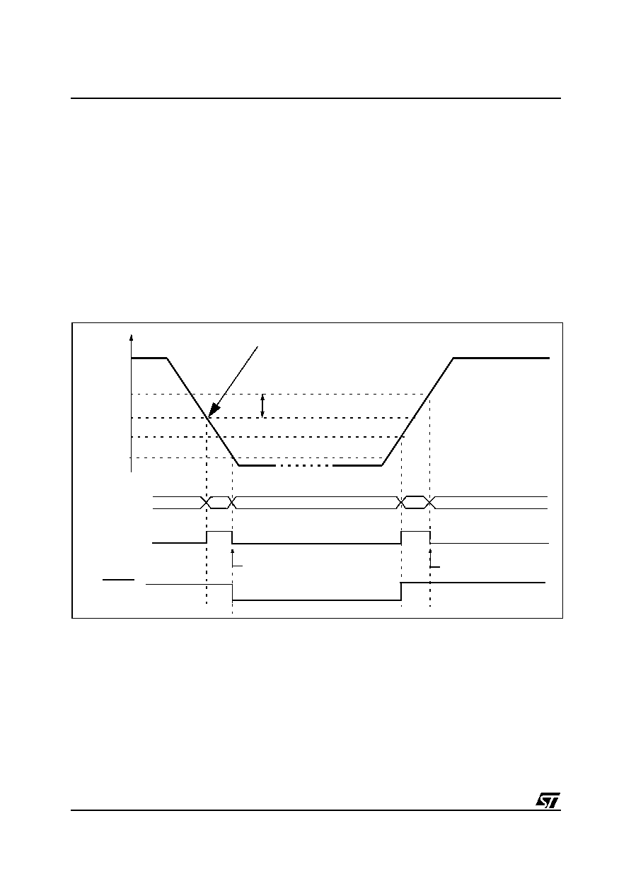
Application notes
The LVDRF flag is not cleared when another RE-
SET type occurs (external or watchdog), the
LVDRF flag remains set to keep trace of the origi-
nal failure.
In this case, a watchdog reset can be detected by
software while an external reset can not.
Table 6. System Integrity Register Map and Reset Values
7
0
0
0
0
0
LOCK
ED
LVDRF AVDF AVDIE
Address
(Hex.)
Register
Label
7
6
5
4
3
2
1
0
003Ah
SICSR
Reset Value
0
0
0
0
LOCKED
0
LVDRF
x
AVDF
0
AVDIE
0
1

ST7LITE0, ST7SUPERLITE
33/122
8 INTERRUPTS
The ST7 core may be interrupted by one of two dif-
ferent methods: maskable hardware interrupts as
listed in the Interrupt Mapping Table and a non-
maskable software interrupt (TRAP). The Interrupt
processing flowchart is shown in
Figure 20
.
The maskable interrupts must be enabled by
clearing the I bit in order to be serviced. However,
disabled interrupts may be latched and processed
when they are enabled (see external interrupts
subsection).
Note: After reset, all interrupts are disabled.
When an interrupt has to be serviced:
≠ Normal processing is suspended at the end of
the current instruction execution.
≠ The PC, X, A and CC registers are saved onto
the stack.
≠ The I bit of the CC register is set to prevent addi-
tional interrupts.
≠ The PC is then loaded with the interrupt vector of
the interrupt to service and the first instruction of
the interrupt service routine is fetched (refer to
the Interrupt Mapping Table for vector address-
es).
The interrupt service routine should finish with the
IRET instruction which causes the contents of the
saved registers to be recovered from the stack.
Note: As a consequence of the IRET instruction,
the I bit will be cleared and the main program will
resume.
Priority Management
By default, a servicing interrupt cannot be inter-
rupted because the I bit is set by hardware enter-
ing in interrupt routine.
In the case when several interrupts are simultane-
ously pending, an hardware priority defines which
one will be serviced first (see the Interrupt Map-
ping Table).
Interrupts and Low Power Mode
All interrupts allow the processor to leave the
WAIT low power mode. Only external and specifi-
cally mentioned interrupts allow the processor to
leave the HALT low power mode (refer to the "Exit
from HALT" column in the Interrupt Mapping Ta-
ble).
8.1 NON MASKABLE SOFTWARE INTERRUPT
This interrupt is entered when the TRAP instruc-
tion is executed regardless of the state of the I bit.
It will be serviced according to the flowchart on
Figure 20
.
8.2 EXTERNAL INTERRUPTS
External interrupt vectors can be loaded into the
PC register if the corresponding external interrupt
occurred and if the I bit is cleared. These interrupts
allow the processor to leave the Halt low power
mode.
The external interrupt polarity is selected through
the miscellaneous register or interrupt register (if
available).
An external interrupt triggered on edge will be
latched and the interrupt request automatically
cleared upon entering the interrupt service routine.
If several input pins, connected to the same inter-
rupt vector, are configured as interrupts, their sig-
nals are logically NANDed before entering the
edge/level detection block.
Caution: The type of sensitivity defined in the Mis-
cellaneous or Interrupt register (if available) ap-
plies to the ei source. In case of a NANDed source
(as described on the I/O ports section), a low level
on an I/O pin configured as input with interrupt,
masks the interrupt request even in case of rising-
edge sensitivity.
8.3 PERIPHERAL INTERRUPTS
Different peripheral interrupt flags in the status
register are able to cause an interrupt when they
are active if both:
≠ The I bit of the CC register is cleared.
≠ The corresponding enable bit is set in the control
register.
If any of these two conditions is false, the interrupt
is latched and thus remains pending.
Clearing an interrupt request is done by:
≠ Writing "0" to the corresponding bit in the status
register or
≠ Access to the status register while the flag is set
followed by a read or write of an associated reg-
ister.
Note: the clearing sequence resets the internal
latch. A pending interrupt (i.e. waiting for being en-
abled) will therefore be lost if the clear sequence is
executed.
1

ST7LITE0, ST7SUPERLITE
34/122
INTERRUPTS (Cont'd)
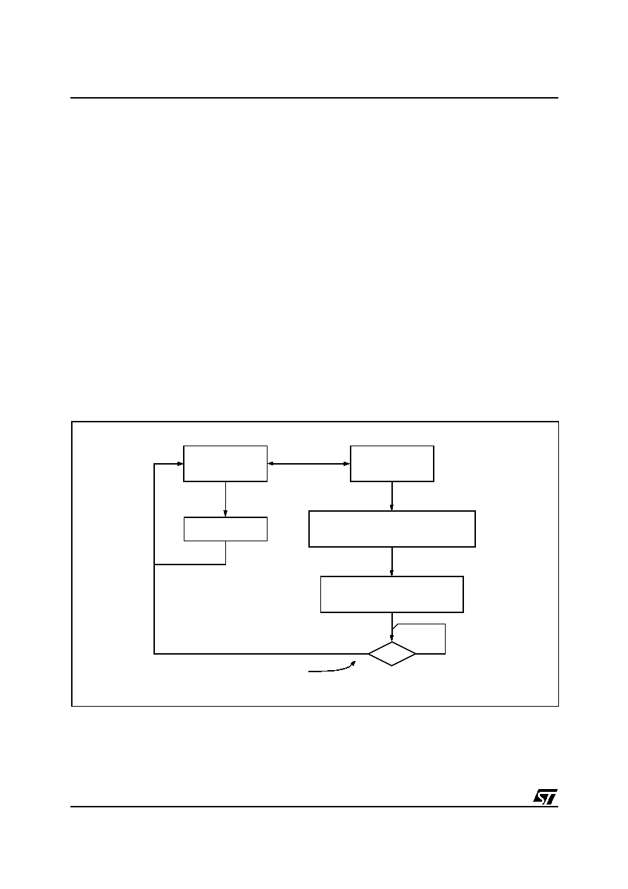
Figure 20. Interrupt Processing Flowchart
Table 7. Interrupt Mapping
I BIT SET?
Y
N
IRET?
Y
N
FROM RESET
LOAD PC FROM INTERRUPT VECTOR
STACK PC, X, A, CC
SET I BIT
FETCH NEXT INSTRUCTION
EXECUTE INSTRUCTION
THIS CLEARS I BIT BY DEFAULT
RESTORE PC, X, A, CC FROM STACK
INTERRUPT
Y
N
PENDING?
N∞
Source
Block
Description
Register
Label
Priority
Order
Exit
from
HALT
Address
Vector
RESET
Reset
N/A
Highest
Priority
Lowest
Priority
yes
FFFEh-FFFFh
TRAP
Software Interrupt
no
FFFCh-FFFDh
0
Not used
FFFAh-FFFBh
1
ei0
External Interrupt 0
yes
FFF8h-FFF9h
2
ei1
External Interrupt 1
FFF6h-FFF7h
3
ei2
External Interrupt 2
FFF4h-FFF5h
4
ei3
External Interrupt 3
FFF2h-FFF3h
5
Not used
FFF0h-FFF1h
6
Not used
FFEEh-FFEFh
7
SI
AVD interrupt
SICSR
yes
FFECh-FFEDh
8
AT TIMER
AT TIMER Output Compare Interrupt
PWM0CSR
no
FFEAh-FFEBh
9
AT TIMER Overflow Interrupt
ATCSR
yes
FFE8h-FFE9h
10
LITE TIMER
LITE TIMER Input Capture Interrupt
LTCSR
no
FFE6h-FFE7h
11
LITE TIMER RTC Interrupt
LTCSR
yes
FFE4h-FFE5h
12
SPI
SPI Peripheral Interrupts
SPICSR
yes
FFE2h-FFE3h
13
Not used
FFE0h-FFE1h
1
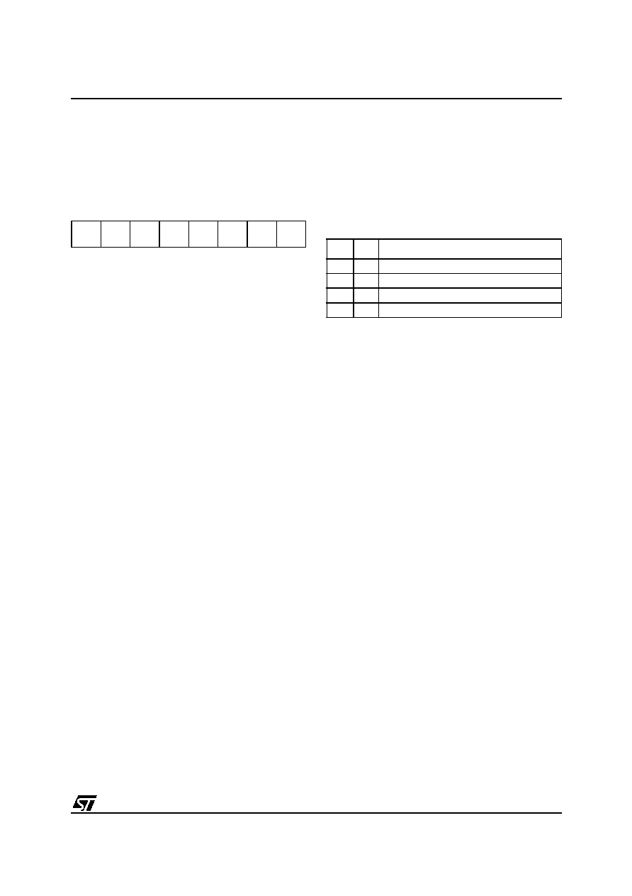
ST7LITE0, ST7SUPERLITE
35/122
INTERRUPTS (Cont'd)
EXTERNAL INTERRUPT CONTROL REGISTER
(EICR)
Read /Write
Reset Value: 0000 0000 (00h)
Bit 7:6 = IS3[1:0]
ei3 sensitivity
These bits define the interrupt sensitivity for ei3
(Port B0) according to
Table 8
.
Bit 5:4 = IS2[1:0]
ei2 sensitivity
These bits define the interrupt sensitivity for ei2
(Port B3) according to
Table 8
.
Bit 3:2 = IS1[1:0]
ei1 sensitivity
These bits define the interrupt sensitivity for ei1
(Port A7) according to
Table 8
.
Bit 1:0 = IS0[1:0]
ei0 sensitivity
These bits define the interrupt sensitivity for ei0
(Port A0) according to
Table 8
.
Note: These 8 bits can be written only when the I
bit in the CC register is set.
Table 8. Interrupt Sensitivity Bits
.
7
0
IS31
IS30
IS21
IS20
IS11
IS10
IS01
IS00
ISx1 ISx0
External Interrupt Sensitivity
0
0
Falling edge & low level
0
1
Rising edge only
1
0
Falling edge only
1
1
Rising and falling edge
1
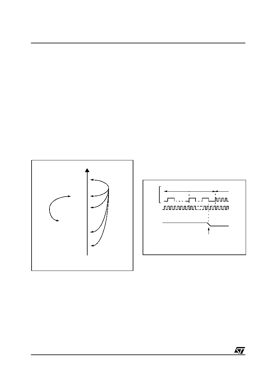
ST7LITE0, ST7SUPERLITE
36/122
9 POWER SAVING MODES
9.1 INTRODUCTION
To give a large measure of flexibility to the applica-
tion in terms of power consumption, four main
power saving modes are implemented in the ST7
(see
Figure 21
): SLOW, WAIT (SLOW WAIT), AC-
TIVE HALT and HALT.
After a RESET the normal operating mode is se-
lected by default (RUN mode). This mode drives
the device (CPU and embedded peripherals) by
means of a master clock which is based on the
main oscillator frequency (f
OSC
).
From RUN mode, the different power saving
modes may be selected by setting the relevant
register bits or by calling the specific ST7 software
instruction whose action depends on the oscillator
status.
Figure 21. Power Saving Mode Transitions
9.2 SLOW MODE
This mode has two targets:
≠ To reduce power consumption by decreasing the
internal clock in the device,
≠ To adapt the internal clock frequency (f
CPU
) to
the available supply voltage.
SLOW mode is controlled by the SMS bit in the
MCCSR register which enables or disables Slow
mode.
In this mode, the oscillator frequency is divided by
32. The CPU and peripherals are clocked at this
lower frequency.
Notes:
SLOW-WAIT mode is activated when entering
WAIT mode while the device is already in SLOW
mode.
SLOW mode has no effect on the Lite Timer which
is already clocked at F
OSC/32
.
Figure 22. SLOW Mode Clock Transition
POWER CONSUMPTION
WAIT
SLOW
RUN
ACTIVE HALT
High
Low
SLOW WAIT
HALT
SMS
f
CPU
NORMAL RUN MODE
REQUEST
f
OSC
f
OSC
/32
f
OSC
1
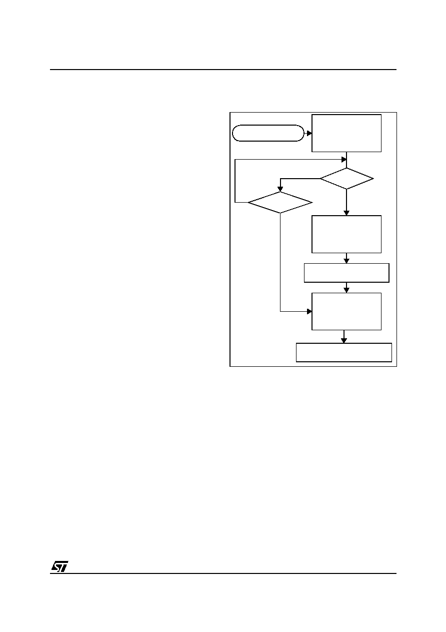
ST7LITE0, ST7SUPERLITE
37/122
POWER SAVING MODES (Cont'd)
9.3 WAIT MODE
WAIT mode places the MCU in a low power con-
sumption mode by stopping the CPU.
This power saving mode is selected by calling the
`WFI' instruction.
All peripherals remain active. During WAIT mode,
the I bit of the CC register is cleared, to enable all
interrupts. All other registers and memory remain
unchanged. The MCU remains in WAIT mode until
an interrupt or RESET occurs, whereupon the Pro-
gram Counter branches to the starting address of
the interrupt or Reset service routine.
The MCU will remain in WAIT mode until a Reset
or an Interrupt occurs, causing it to wake up.
Refer to
Figure 23
.
Figure 23. WAIT Mode Flow-chart
Note:
1. Before servicing an interrupt, the CC register is
pushed on the stack. The I bit of the CC register is
set during the interrupt routine and cleared when
the CC register is popped.
WFI INSTRUCTION
RESET
INTERRUPT
Y
N
N
Y
CPU
OSCILLATOR
PERIPHERALS
I BIT
ON
ON
0
OFF
FETCH RESET VECTOR
OR SERVICE INTERRUPT
CPU
OSCILLATOR
PERIPHERALS
I BIT
ON
OFF
0
ON
CPU
OSCILLATOR
PERIPHERALS
I BIT
ON
ON
X
1)
ON
256 CPU CLOCK CYCLE
DELAY
1
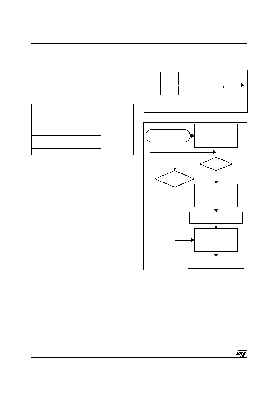
ST7LITE0, ST7SUPERLITE
38/122
POWER SAVING MODES (Cont'd)
9.4 ACTIVE-HALT AND HALT MODES
ACTIVE-HALT and HALT modes are the two low-
est power consumption modes of the MCU. They
are both entered by executing the `HALT' instruc-
tion. The decision to enter either in ACTIVE-HALT
or HALT mode is given by the LTCSR/ATCSR reg-
ister status as shown in the following table:.
9.4.1 ACTIVE-HALT MODE
ACTIVE-HALT mode is the lowest power con-
sumption mode of the MCU with a real time clock
available. It is entered by executing the `HALT' in-
struction when active halt mode is enabled.
The MCU can exit ACTIVE-HALT mode on recep-
tion of a Lite Timer / AT Timer interrupt or a RE-
SET.
≠ When exiting ACTIVE-HALT mode by means of
a RESET, a 256 CPU cycle delay occurs. After
the start up delay, the CPU resumes operation
by fetching the reset vector which woke it up (see
Figure 25
).
≠ When exiting ACTIVE-HALT mode by means of
an interrupt, the CPU immediately resumes oper-
ation by servicing the interrupt vector which woke
it up (see
Figure 25
).
When entering ACTIVE-HALT mode, the I bit in
the CC register is cleared to enable interrupts.
Therefore, if an interrupt is pending, the MCU
wakes up immediately.
In ACTIVE-HALT mode, only the main oscillator
and the selected timer counter (LT/AT) are running
to keep a wake-up time base. All other peripherals
are not clocked except those which get their clock
supply from another clock generator (such as ex-
ternal or auxiliary oscillator).
Caution: As soon as ACTIVE-HALT is enabled,
executing a HALT instruction while the Watchdog
is active does not generate a RESET if the
WDGHALT bit is reset.
This means that the device cannot spend more
than a defined delay in this power saving mode.
Figure 24. ACTIVE-HALT Timing Overview
Figure 25. ACTIVE-HALT Mode Flow-chart
Notes:
1. This delay occurs only if the MCU exits ACTIVE-
HALT mode by means of a RESET.
2. Peripherals clocked with an external clock
source can still be active.
3. Only the Lite Timer RTC and AT Timer interrupts
can exit the MCU from ACTIVE-HALT mode.
4. Before servicing an interrupt, the CC register is
pushed on the stack. The I bit of the CC register is
set during the interrupt routine and cleared when
the CC register is popped.
LTCSR
TBIE bit
ATCSR
OVFIE
bit
ATCSR
CK1 bit
ATCSR
CK0 bit
Meaning
0
x
x
0
ACTIVE-HALT
mode disabled
0
0
x
x
0
1
1
1
1
x
x
x
ACTIVE-HALT
mode enabled
x
1
0
1
HALT
RUN
RUN
256 CPU
CYCLE DELAY
1)
RESET
OR
INTERRUPT
HALT
INSTRUCTION
FETCH
VECTOR
ACTIVE
[Active Halt Enabled]
HALT INSTRUCTION
RESET
INTERRUPT
3)
Y
N
N
Y
CPU
OSCILLATOR
PERIPHERALS
2)
I BIT
ON
OFF
0
OFF
FETCH RESET VECTOR
OR SERVICE INTERRUPT
CPU
OSCILLATOR
PERIPHERALS
2)
I BIT
ON
OFF
X
4)
ON
CPU
OSCILLATOR
PERIPHERALS
I BITS
ON
ON
X
4)
ON
256 CPU CLOCK CYCLE
DELAY
(Active Halt enabled)
1
ST7LITE0, ST7SUPERLITE
39/122
POWER SAVING MODES (Cont'd)
9.4.2 HALT MODE
The HALT mode is the lowest power consumption
mode of the MCU. It is entered by executing the
`HALT' instruction when active halt mode is disa-
bled.
The MCU can exit HALT mode on reception of ei-
ther a specific interrupt (see Table 7, "Interrupt
Mapping," on page 34) or a RESET. When exiting
HALT mode by means of a RESET or an interrupt,
the oscillator is immediately turned on and the 256
CPU cycle delay is used to stabilize the oscillator.
After the start up delay, the CPU resumes opera-
tion by servicing the interrupt or by fetching the re-
set vector which woke it up (see
Figure 27
).
When entering HALT mode, the I bit in the CC reg-
ister is forced to 0 to enable interrupts. Therefore,
if an interrupt is pending, the MCU wakes immedi-
ately.
In HALT mode, the main oscillator is turned off
causing all internal processing to be stopped, in-
cluding the operation of the on-chip peripherals.
All peripherals are not clocked except the ones
which get their clock supply from another clock
generator (such as an external or auxiliary oscilla-
tor).
The compatibility of Watchdog operation with
HALT mode is configured by the "WDGHALT" op-
tion bit of the option byte. The HALT instruction
when executed while the Watchdog system is en-
abled, can generate a Watchdog RESET (see
sec-
tion 15.1 on page 109
for more details).
Figure 26. HALT Timing Overview
Figure 27. HALT Mode Flow-chart
Notes:
1. WDGHALT is an option bit. See option byte sec-
tion for more details.
2. Peripheral clocked with an external clock source
can still be active.
3. Only some specific interrupts can exit the MCU
from HALT mode (such as external interrupt). Re-
fer to Table 7, "Interrupt Mapping," on page 34 for
more details.
4. Before servicing an interrupt, the CC register is
pushed on the stack. The I bit of the CC register is
set during the interrupt routine and cleared when
the CC register is popped.
5. If the PLL is enabled by option byte, it outputs
the clock after a delay of t
STARTUP
(see
Figure 12
).
HALT
RUN
RUN
256 CPU CYCLE
DELAY
RESET
OR
INTERRUPT
HALT
INSTRUCTION
FETCH
VECTOR
[Active Halt disabled]
HALT INSTRUCTION
RESET
INTERRUPT
3)
Y
N
N
Y
CPU
OSCILLATOR
PERIPHERALS
2)
I BIT
OFF
OFF
0
OFF
FETCH RESET VECTOR
OR SERVICE INTERRUPT
CPU
OSCILLATOR
PERIPHERALS
I BIT
ON
OFF
X
4)
ON
CPU
OSCILLATOR
PERIPHERALS
I BITS
ON
ON
X
4)
ON
256 CPU CLOCK CYCLE
DELAY
WATCHDOG
ENABLE
DISABLE
WDGHALT
1)
0
WATCHDOG
RESET
1
(Active Halt disabled)
1

ST7LITE0, ST7SUPERLITE
40/122
POWER SAVING MODES (Cont'd)
9.4.2.1 HALT Mode Recommendations
≠ Make sure that an external event is available to
wake up the microcontroller from Halt mode.
≠ When using an external interrupt to wake up the
microcontroller, reinitialize the corresponding I/O
as "Input Pull-up with Interrupt" before executing
the HALT instruction. The main reason for this is
that the I/O may be wrongly configured due to ex-
ternal interference or by an unforeseen logical
condition.
≠ For the same reason, reinitialize the level sensi-
tiveness of each external interrupt as a precau-
tionary measure.
≠ The opcode for the HALT instruction is 0x8E. To
avoid an unexpected HALT instruction due to a
program counter failure, it is advised to clear all
occurrences of the data value 0x8E from memo-
ry. For example, avoid defining a constant in
ROM with the value 0x8E.
≠ As the HALT instruction clears the I bit in the CC
register to allow interrupts, the user may choose
to clear all pending interrupt bits before execut-
ing the HALT instruction. This avoids entering
other peripheral interrupt routines after executing
the external interrupt routine corresponding to
the wake-up event (reset or external interrupt).
1
ST7LITE0, ST7SUPERLITE
41/122
10 I/O PORTS
10.1 INTRODUCTION
The I/O ports offer different functional modes:
≠ transfer of data through digital inputs and outputs
and for specific pins:
≠ external interrupt generation
≠ alternate signal input/output for the on-chip pe-
ripherals.
An I/O port contains up to 8 pins. Each pin can be
programmed independently as digital input (with or
without interrupt generation) or digital output.
10.2 FUNCTIONAL DESCRIPTION
Each port has 2 main registers:
≠ Data Register (DR)
≠ Data Direction Register (DDR)
and one optional register:
≠ Option Register (OR)
Each I/O pin may be programmed using the corre-
sponding register bits in the DDR and OR regis-
ters: bit X corresponding to pin X of the port. The
same correspondence is used for the DR register.
The following description takes into account the
OR register, (for specific ports which do not pro-
vide this register refer to the I/O Port Implementa-
tion section). The generic I/O block diagram is
shown in
Figure 28
10.2.1 Input Modes
The input configuration is selected by clearing the
corresponding DDR register bit.
In this case, reading the DR register returns the
digital value applied to the external I/O pin.
Different input modes can be selected by software
through the OR register.
Note: Writing the DR register modifies the latch
value but does not affect the pin status.
External interrupt function
When an I/O is configured as Input with Interrupt,
an event on this I/O can generate an external inter-
rupt request to the CPU.
Each pin can independently generate an interrupt
request. The interrupt sensitivity is independently
programmable using the sensitivity bits in the
EICR register.
Each external interrupt vector is linked to a dedi-
cated group of I/O port pins (see pinout description
and interrupt section). If several input pins are se-
lected simultaneously as interrupt source, these
are logically ANDed. For this reason if one of the
interrupt pins is tied low, it masks the other ones.
The external interrupts are hardware interrupts,
which means that the request latch (not accessible
directly by the application) is automatically cleared
when the corresponding interrupt vector is
fetched. To clear an unwanted pending interrupt
by software, the sensitivity bits in the EICR register
must be modified.
10.2.2 Output Modes
The output configuration is selected by setting the
corresponding DDR register bit. In this case, writ-
ing the DR register applies this digital value to the
I/O pin through the latch. Then reading the DR reg-
ister returns the previously stored value.
Two different output modes can be selected by
software through the OR register: Output push-pull
and open-drain.
DR register value and output pin status:
Note: When switching from input to output mode,
the DR register has to be written first to drive the
correct level on the pin as soon as the port is con-
figured as an output.
10.2.3 Alternate Functions
When an on-chip peripheral is configured to use a
pin, the alternate function is automatically select-
ed. This alternate function takes priority over the
standard I/O programming under the following
conditions:
≠ When the signal is coming from an on-chip pe-
ripheral, the I/O pin is automatically configured in
output mode (push-pull or open drain according
to the peripheral).
≠ When the signal is going to an on-chip peripher-
al, the I/O pin must be configured in floating input
mode. In this case, the pin state is also digitally
readable by addressing the DR register.
Notes:
≠ Input pull-up configuration can cause unexpect-
ed value at the input of the alternate peripheral
input.
≠ When an on-chip peripheral use a pin as input
and output, this pin has to be configured in input
floating mode.
DR
Push-pull
Open-drain
0
V
SS
Vss
1
V
DD
Floating
1
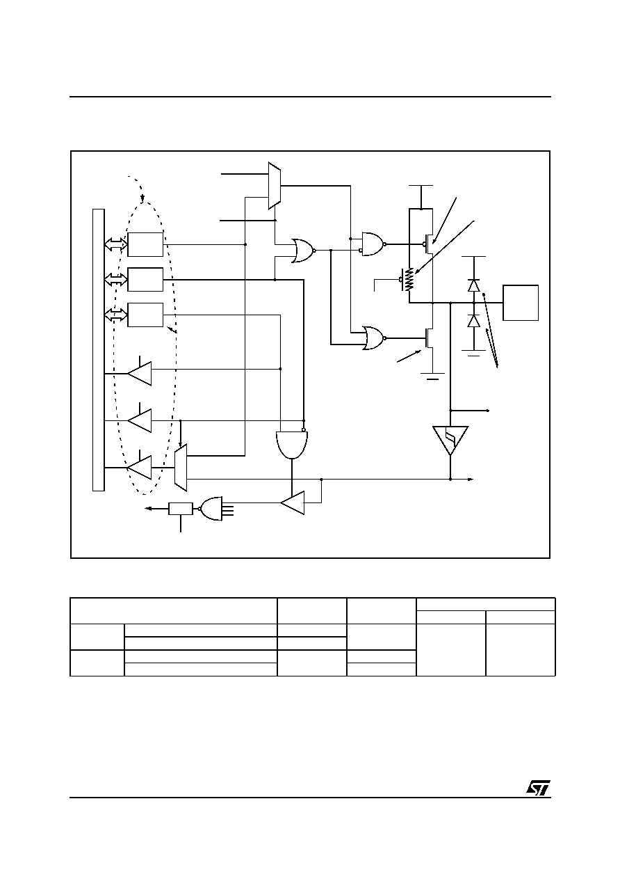
ST7LITE0, ST7SUPERLITE
42/122
I/O PORTS (Cont'd)
Figure 28. I/O Port General Block Diagram
Table 9. I/O Port Mode Options
Legend: NI - not implemented
Off - implemented not activated
On - implemented and activated
Configuration Mode
Pull-Up
P-Buffer
Diodes
to V
DD
to V
SS
Input
Floating with/without Interrupt
Off
Off
On
On
Pull-up with/without Interrupt
On
Output
Push-pull
Off
On
Open Drain (logic level)
Off
DR
DDR
OR
DA
T
A
B
U
S
PAD
V
DD
ALTERNATE
ENABLE
ALTERNATE
OUTPUT
1
0
OR SEL
DDR SEL
DR SEL
PULL-UP
CONDITION
P-BUFFER
(see table below)
N-BUFFER
PULL-UP
(see table below)
1
0
ANALOG
INPUT
If implemented
ALTERNATE
INPUT
V
DD
DIODES
(see table below)
FROM
OTHER
BITS
EXTERNAL
SOURCE (ei
x
)
INTERRUPT
POLARITY
SELECTION
CMOS
SCHMITT
TRIGGER
REGISTER
ACCESS
1
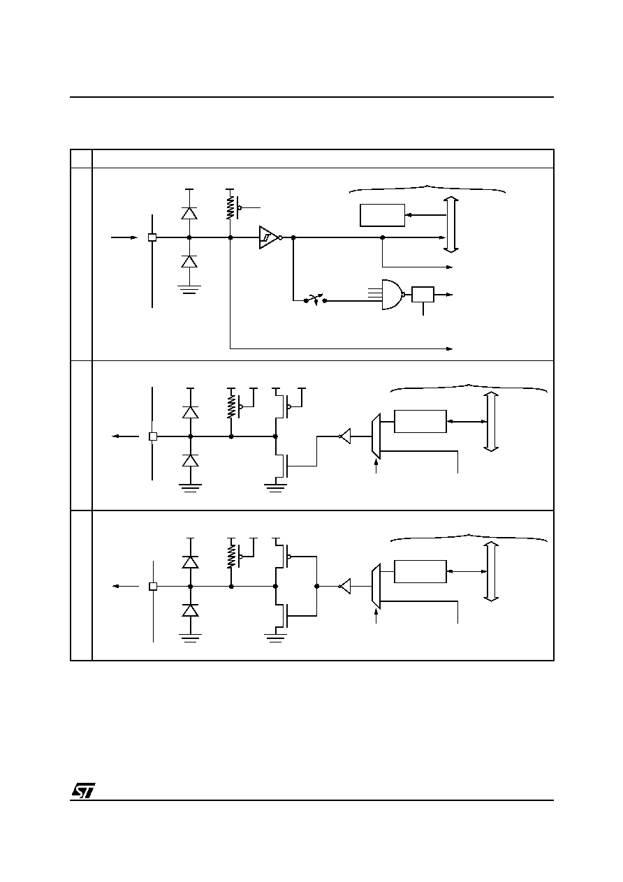
ST7LITE0, ST7SUPERLITE
43/122
I/O PORTS (Cont'd)
Table 10. I/O Port Configurations
Notes:
1. When the I/O port is in input configuration and the associated alternate function is enabled as an output,
reading the DR register will read the alternate function output status.
2. When the I/O port is in output configuration and the associated alternate function is enabled as an input,
the alternate function reads the pin status given by the DR register content.
Hardware Configuration
I
NPUT
1)
O
PEN-
DRAI
N
O
U
TPUT
2)
PUS
H-PU
LL
O
UTPU
T
2)
CONDITION
PAD
V
DD
R
PU
EXTERNAL INTERRUPT
POLARITY
DATA BUS
PULL-UP
INTERRUPT
DR REGISTER ACCESS
W
R
FROM
OTHER
PINS
SOURCE (ei
x
)
SELECTION
DR
REGISTER
CONDITION
ALTERNATE INPUT
ANALOG INPUT
PAD
R
PU
DATA BUS
DR
DR REGISTER ACCESS
R/W
V
DD
ALTERNATE
ALTERNATE
ENABLE
OUTPUT
REGISTER
PAD
R
PU
DATA BUS
DR
DR REGISTER ACCESS
R/W
V
DD
ALTERNATE
ALTERNATE
ENABLE
OUTPUT
REGISTER
1
ST7LITE0, ST7SUPERLITE
44/122
I/O PORTS (Cont'd)
CAUTION: The alternate function must not be ac-
tivated as long as the pin is configured as input
with interrupt, in order to avoid generating spurious
interrupts.
Analog alternate function
When the pin is used as an ADC input, the I/O
must be configured as floating input. The analog
multiplexer (controlled by the ADC registers)
switches the analog voltage present on the select-
ed pin to the common analog rail which is connect-
ed to the ADC input.
It is recommended not to change the voltage level
or loading on any port pin while conversion is in
progress. Furthermore it is recommended not to
have clocking pins located close to a selected an-
alog pin.
WARNING: The analog input voltage level must
be within the limits stated in the absolute maxi-
mum ratings.
10.3 UNUSED I/O PINS
Unused I/O pins must be connected to fixed volt-
age levels. Refer to
Section 13.8
.
10.4 LOW POWER MODES
10.5 INTERRUPTS
The external interrupt event generates an interrupt
if the corresponding configuration is selected with
DDR and OR registers and the interrupt mask in
the CC register is not active (RIM instruction).
10.6 I/O PORT IMPLEMENTATION
The hardware implementation on each I/O port de-
pends on the settings in the DDR and OR registers
and specific feature of the I/O port such as ADC In-
put or true open drain.
Switching these I/O ports from one state to anoth-
er should be done in a sequence that prevents un-
wanted side effects. Recommended safe transi-
tions are illustrated in
Figure 29
Other transitions
are potentially risky and should be avoided, since
they are likely to present unwanted side-effects
such as spurious interrupt generation.
Figure 29. Interrupt I/O Port State Transitions
The I/O port register configurations are summa-
rised as follows.
Table 11. Port Configuration
Mode Description
WAIT
No effect on I/O ports. External interrupts
cause the device to exit from WAIT mode.
HALT
No effect on I/O ports. External interrupts
cause the device to exit from HALT mode.
Interrupt Event
Event
Flag
Enable
Control
Bit
Exit
from
Wait
Exit
from
Halt
External interrupt on
selected external
event
-
DDRx
ORx
Yes
Yes
01
floating/pull-up
interrupt
INPUT
00
floating
(reset state)
INPUT
10
open-drain
OUTPUT
11
push-pull
OUTPUT
XX
= DDR, OR
Port
Pin name
Input (DDR=0)
Output (DDR=1)
OR = 0
OR = 1
OR = 0
OR = 1
Port A
PA7
floating
pull-up interrupt
open drain
push-pull
PA6:1
floating
pull-up
open drain
push-pull
PA0
floating
pull-up interrupt
open drain
push-pull
Port B
PB4
floating
pull-up
open drain
push-pull
PB3
floating
pull-up interrupt
open drain
push-pull
PB2:1
floating
pull-up
open drain
push-pull
PB0
floating
pull-up interrupt
open drain
push-pull
1

ST7LITE0, ST7SUPERLITE
45/122
I/O PORTS (Cont'd)
Table 12. I/O Port Register Map and Reset Values
Address
(Hex.)
Register
Label
7
6
5
4
3
2
1
0
0000h
PADR
Reset Value
MSB
0
0
0
0
0
0
0
LSB
0
0001h
PADDR
Reset Value
MSB
0
0
0
0
0
0
0
LSB
0
0002h
PAOR
Reset Value
MSB
0
1
0
0
0
0
0
LSB
0
0003h
PBDR
Reset Value
MSB
1
1
1
0
0
0
0
LSB
0
0004h
PBDDR
Reset Value
MSB
0
0
0
0
0
0
0
LSB
0
0005h
PBOR
Reset Value
MSB
0
0
0
0
0
0
0
LSB
0
1
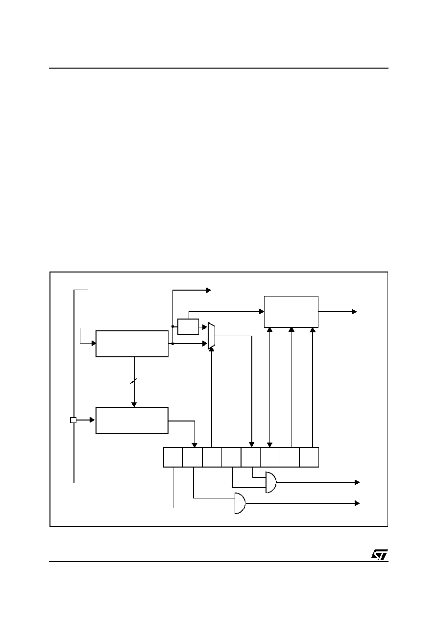
ST7LITE0, ST7SUPERLITE
46/122
11 ON-CHIP PERIPHERALS
11.1 LITE TIMER (LT)
11.1.1 Introduction
The Lite Timer can be used for general-purpose
timing functions. It is based on a free-running 8-bit
upcounter with two software-selectable timebase
periods, an 8-bit input capture register and watch-
dog function.
11.1.2 Main Features
s
Realtime Clock
≠ 8-bit upcounter
≠ 1 ms or 2 ms timebase period (@ 8 MHz f
OSC
)
≠ Maskable timebase interrupt
s
Input Capture
≠ 8-bit input capture register (LTICR)
≠ Maskable interrupt with wakeup from Halt
Mode capability
s
Watchdog
≠ Enabled by hardware or software (configura-
ble by option byte)
≠ Optional reset on HALT instruction (configura-
ble by option byte)
≠ Automatically resets the device unless disable
bit is refreshed
≠ Software reset (Forced Watchdog reset)
≠ Watchdog reset status flag
Figure 30. Lite Timer Block Diagram
LTCSR
WATCHDOG
8-bit UPCOUNTER
/2
8-bit
f
LTIMER
f
WDG
8
LTIC
f
OSC
/32
WDGD
WDGE
WDG
TBF
TBIE
TB
ICF
ICIE
WATCHDOG RESET
LTTB INTERRUPT REQUEST
LTIC INTERRUPT REQUEST
LTICR
INPUT CAPTURE
REGISTER
1
0
1 or 2 ms
Timebase
(@ 8MHz
f
OSC
)
To 12-bit AT TImer
f
LTIMER
RF
0
7
1

ST7LITE0, ST7SUPERLITE
47/122
LITE TIMER (Cont'd)
11.1.3 Functional Description
The value of the 8-bit counter cannot be read or
written by software. After an MCU reset, it starts
incrementing from 0 at a frequency of f
OSC
/32. A
counter overflow event occurs when the counter
rolls over from F9h to 00h. If f
OSC
= 8 MHz, then
the time period between two counter overflow
events is 1 ms. This period can be doubled by set-
ting the TB bit in the LTCSR register.
When the timer overflows, the TBF bit is set by
hardware and an interrupt request is generated if
the TBIE is set. The TBF bit is cleared by software
reading the LTCSR register.
11.1.3.1 Watchdog
The watchdog is enabled using the WDGE bit.
The normal Watchdog timeout is 2ms (@ = 8 MHz
f
OSC
), after which it then generates a reset.
To prevent this watchdog reset occuring, software
must set the WDGD bit. The WDGD bit is cleared
by hardware after t
WDG
. This means that software
must write to the WDGD bit at regular intervals to
prevent a watchdog reset occurring. Refer to
Fig-
ure 31
.
If the watchdog is not enabled immediately after
reset, the first watchdog timeout will be shorter
than 2ms, because this period is counted starting
from reset. Moreover, if a 2ms period has already
elapsed after the last MCU reset, the watchdog re-
set will take place as soon as the WDGE bit is set.
For these reasons, it is recommended to enable
the Watchdog immediately after reset or else to
set the WDGD bit before the WGDE bit so a
watchdog reset will not occur for at least 2ms.
Note: Software can use the timebase feature to
set the WDGD bit at 1 or 2 ms intervals.
A Watchdog reset can be forced at any time by
setting the WDGRF bit. To generate a forced
watchdog reset, first watchdog has to be activated
by setting the WDGE bit and then the WDGRF bit
has to be set.
The WDGRF bit also acts as a flag, indicating that
the Watchdog was the source of the reset. It is au-
tomatically cleared after it has been read.
Caution: When the WDGRF bit is set, software
must clear it, otherwise the next time the watchdog
is enabled (by hardware or software), the micro-
controller will be immediately reset.
Hardware Watchdog Option
If Hardware Watchdog is selected by option byte,
the watchdog is always active and the WDGE bit in
the LTCSR is not used.
Refer to the Option Byte description in the "device
configuration and ordering information" section.
Using Halt Mode with the Watchdog (option)
If the Watchdog reset on HALT option is not se-
lected by option byte, the Halt mode can be used
when the watchdog is enabled.
In this case, the HALT instruction stops the oscilla-
tor. When the oscillator is stopped, the Lite Timer
stops counting and is no longer able to generate a
Watchdog reset until the microcontroller receives
an external interrupt or a reset.
If an external interrupt is received, the WDG re-
starts counting after 256 CPU clocks. If a reset is
generated, the Watchdog is disabled (reset state).
If Halt mode with Watchdog is enabled by option
byte (No watchdog reset on HALT instruction), it is
recommended before executing the HALT instruc-
tion to refresh the WDG counter, to avoid an unex-
pected WDG reset immediately after waking up
the microcontroller.
1
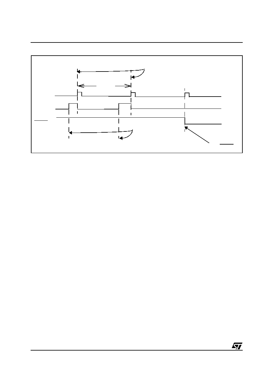
ST7LITE0, ST7SUPERLITE
48/122
Figure 31. Watchdog Timing Diagram
t
WDG
f
WDG
INTERNAL
WATCHDOG
RESET
WDGD BIT
SOFTWARE SETS
WDGD BIT
HARDWARE CLEARS
WDGD BIT
WATCHDOG RESET
(2ms @ 8MHz f
OSC
)
1

ST7LITE0, ST7SUPERLITE
49/122
LITE TIMER (Cont'd)
Input Capture
The 8-bit input capture register is used to latch the
free-running upcounter after a rising or falling edge
is detected on the ICAP1 pin. When an input cap-
ture occurs, the ICF bit is set and the LTICR regis-
ter contains the MSB of the free-running up-
counter. An interrupt is generated if the ICIE bit is
set. The ICF bit is cleared by reading the LTICR
register.
The LTICR is a read only register and always con-
tains the data from the last input capture. Input
capture is inhibited if the ICF bit is set.
11.1.4 Low Power Modes
11.1.5 Interrupts
Note: The TBF and ICF interrupt events are con-
nected to separate interrupt vectors (see Inter-
rupts chapter).
They generate an interrupt if the enable bit is set in
the LTCSR register and the interrupt mask in the
CC register is reset (RIM instruction).
Figure 32. Input Capture Timing Diagram.
Mode Description
SLOW
No effect on Lite timer
(this peripheral is driven directly
by f
OSC
/32)
WAIT
No effect on Lite timer
ACTIVE-HALT No effect on Lite timer
HALT
Lite timer stops counting
Interrupt
Event
Event
Flag
Enable
Control
Bit
Exit
from
Wait
Exit
from
Halt
Exit
from
Active-
Halt
Timebase
Event
TBF
TBIE
Yes
No
Yes
IC Event
ICF
ICIE
Yes
No
No
04h
8-bit COUNTER
t
01h
f
OSC
/32
xxh
02h
03h
05h
06h
07h
04h
LTIC PIN
ICF FLAG
LTICR REGISTER
CLEARED
4µs
(@ 8MHz f
OSC
)
f
CPU
BY S/W
07h
READING
LTIC REGISTER
1
ST7LITE0, ST7SUPERLITE
50/122
LITE TIMER (Cont'd)
11.1.6 Register Description
LITE TIMER CONTROL/STATUS REGISTER
(LTCSR)
Read / Write
Reset Value: 0x00 0000 (x0h)
Bit 7 = ICIE
Interrupt Enable.
This bit is set and cleared by software.
0: Input Capture (IC) interrupt disabled
1: Input Capture (IC) interrupt enabled
Bit 6 = ICF
Input Capture Flag.
This bit is set by hardware and cleared by software
by reading the LTICR register. Writing to this bit
does not change the bit value.
0: No input capture
1: An input capture has occurred
Note: After an MCU reset, software must initialise
the ICF bit by reading the LTICR register
Bit 5 = TB
Timebase period selection.
This bit is set and cleared by software.
0: Timebase period = t
OSC
* 8000 (1ms @ 8 MHz)
1: Timebase period = t
OSC
* 16000 (2ms @ 8
MHz)
Bit 4 = TBIE
Timebase Interrupt enable
.
This bit is set and cleared by software.
0: Timebase (TB) interrupt disabled
1: Timebase (TB) interrupt enabled
Bit 3 = TBF
Timebase Interrupt Flag
.
This bit is set by hardware and cleared by software
reading the LTCSR register. Writing to this bit has
no effect.
0: No counter overflow
1: A counter overflow has occurred
Bit 2 = WDGRF
Force Reset/ Reset Status Flag
This bit is used in two ways: it is set by software to
force a watchdog reset. It is set by hardware when
a watchdog reset occurs and cleared by hardware
or by software. It is cleared by hardware only when
an LVD reset occurs. It can be cleared by software
after a read access to the LTCSR register.
0: No watchdog reset occurred.
1: Force a watchdog reset (write), or, a watchdog
reset occurred (read).
Bit 1 = WDGE
Watchdog Enable
This bit is set and cleared by software.
0: Watchdog disabled
1: Watchdog enabled
Bit 0 = WDGD
Watchdog Reset Delay
This bit is set by software. It is cleared by hard-
ware at the end of each t
WDG
period.
0: Watchdog reset not delayed
1: Watchdog reset delayed
LITE TIMER INPUT CAPTURE REGISTER
(LTICR)
Read only
Reset Value: 0000 0000 (00h)
Bit 7:0 = ICR[7:0]
Input Capture Value
These bits are read by software and cleared by
hardware after a reset. If the ICF bit in the LTCSR
is cleared, the value of the 8-bit up-counter will be
captured when a rising or falling edge occurs on
the LTIC pin.
Table 13. Lite Timer Register Map and Reset Values
7
0
ICIE
ICF
TB
TBIE
TBF
WDGR WDGE WDGD
7
0
ICR7
ICR6
ICR5
ICR4
ICR3
ICR2
ICR1
ICR0
Address
(Hex.)
Register
Label
7
6
5
4
3
2
1
0
0B
LTCSR
Reset Value
ICIE
0
ICF
x
TB
0
TBIE
0
TBF
0
WDGRF
0
WDGE
0
WDGD
0
0C
LTICR
Reset Value
ICR7
0
ICR6
0
ICR5
0
ICR4
0
ICR3
0
ICR2
0
ICR1
0
ICR0
0
1
ST7LITE0, ST7SUPERLITE
51/122
11.2 12-BIT AUTORELOAD TIMER (AT)
11.2.1 Introduction
The 12-bit Autoreload Timer can be used for gen-
eral-purpose timing functions. It is based on a free-
running 12-bit upcounter with a PWM output chan-
nel.
11.2.2 Main Features
s
12-bit upcounter with 12-bit autoreload register
(ATR)
s
Maskable overflow interrupt
s
PWM signal generator
s
Frequency range 2KHz-4MHz (@ 8 MHz f
CPU
)
≠ Programmable duty-cycle
≠ Polarity control
≠ Maskable Compare interrupt
s
Output Compare Function
Figure 33. Block Diagram
ATCSR
CMPIE
OVFIE
OVF
CK0
CK1
0
0
0
12-BIT AUTORELOAD VALUE
12-BIT UPCOUNTER
CMPF0 bit
CMPF0
CMP INTERRUPT
REQUEST
OVF INTERRUPT
REQUEST
f
CPU
ATR
PWM
GEN
ERAT
ION
POL-
ARITY
OP0 bit
PWM0
COMP-
PARE
f
COUNTER
f
PWM
OUT
PUT CONT
ROL
OE0 bit
CNTR
(1 ms timebase
f
LTIMER
DCR0H
DCR0L
Update on OVF Event
Preload
Preload
@ 8MHz)
7
0
on OVF Event
0
1
12-BIT DUTY CYCLE VALUE (shadow)
OE0 bit
IF OE0=1
1
ST7LITE0, ST7SUPERLITE
52/122
12-BIT AUTORELOAD TIMER (Cont'd)
11.2.3 Functional Description
PWM Mode
This mode allows a Pulse Width Modulated sig-
nals to be generated on the PWM0 output pin with
minimum core processing overhead. The PWM0
output signal can be enabled or disabled using the
OE0 bit in the PWMCR register. When this bit is
set the PWM I/O pin is configured as output push-
pull alternate function.
Note: CMPF0 is available in PWM mode (see
PWM0CSR description on
page 55
).
PWM Frequency and Duty Cycle
The PWM signal frequency (f
PWM
) is controlled by
the counter period and the ATR register value.
f
PWM
= f
COUNTER
/ (4096 - ATR)
Following the above formula, if f
CPU
is 8 MHz, the
maximum value of f
PWM
is 4 Mhz (ATR register
value = 4094), and the minimum value is 2 kHz
(ATR register value = 0).
Note: The maximum value of ATR is 4094 be-
cause it must be lower than the DCR value which
must be 4095 in this case.
At reset, the counter starts counting from 0.
Software must write the duty cycle value in the
DCR0H and DCR0L preload registers. The
DCR0H register must be written first. See caution
below.
When a upcounter overflow occurs (OVF event),
the ATR value is loaded in the upcounter, the
preloaded Duty cycle value is transferred to the
Duty Cycle register and the PWM0 signal is set to
a high level. When the upcounter matches the
DCRx value the PWM0 signals is set to a low level.
To obtain a signal on the PWM0 pin, the contents
of the DCR0 register must be greater than the con-
tents of the ATR register.
The polarity bit can be used to invert the output
signal.
The maximum available resolution for the PWM0
duty cycle is:
Resolution = 1 / (4096 - ATR)
Note: To get the maximum resolution (1/4096), the
ATR register must be 0. With this maximum reso-
lution and assuming that DCR=ATR, a 0% or
100% duty cycle can be obtained by changing the
polarity .
Caution: As soon as the DCR0H is written, the
compare function is disabled and will start only
when the DCR0L value is written. If the DCR0H
write occurs just before the compare event, the
signal on the PWM output may not be set to a low
level. In this case, the DCRx register should be up-
dated just after an OVF event. If the DCR and ATR
values are close, then the DCRx register shouldbe
updated just before an OVF event, in order not to
miss a compare event and to have the right signal
applied on the PWM output.
Figure 34. PWM Function
DUTY CYCLE
REGISTER
AUTO-RELOAD
REGISTER
PWM
0
O
U
T
P
U
T
t
4095
000
WITH OE0=1
AND OP0=0
(ATR)
(DCR0)
WITH OE0=1
AND OP0=1
CO
U
N
T
E
R
1
ST7LITE0, ST7SUPERLITE
53/122
12-BIT AUTORELOAD TIMER (Cont'd)
Figure 35. PWM Signal Example
Output Compare Mode
To use this function, the OE bit must be 0, other-
wise the compare is done with the shadow register
instead of the DCRx register. Software must then
write a 12-bit value in the DCR0H and DCR0L reg-
isters. This value will be loaded immediately (with-
out waiting for an OVF event).
The DCR0H must be written first, the output com-
pare function starts only when the DCR0L value is
written.
When the 12-bit upcounter (CNTR) reaches the
value stored in the DCR0H and DCR0L registers,
the CMPF0 bit in the PWM0CSR register is set
and an interrupt request is generated if the CMPIE
bit is set.
Note: The output compare function is only availa-
ble for DCRx values other than 0 (reset value).
Caution: At each OVF event, the DCRx value is
written in a shadow register, even if the DCR0L
value has not yet been written (in this case, the
shadow register will contain the new DCR0H value
and the old DCR0L value), then:
≠ If OE=1 (PWM mode): the compare is done be-
tween the timer counter and the shadow register
(and not DCRx)
≠ if OE=0 (OCMP mode): the compare is done be-
tween the timer counter and DCRx. There is no
PWM signal.
The compare between DCRx or the shadow regis-
ter and the timer counter is locked until DCR0L is
written.
11.2.4 Low Power Modes
11.2.5 Interrupts
Note 1: The interrupt events are connected to sep-
arate interrupt vectors (see Interrupts chapter).
They generate an interrupt if the enable bit is set in
the ATCSR register and the interrupt mask in the
CC register is reset (RIM instruction).
Note 2: only if CK0=1and CK1=0
COUNTER
PW
M
0
O
U
T
P
U
T
t
WI
T
H
O
E
0
=
1
AN
D
O
P
0
=
0
FFDh
FFEh
FFFh
FFDh
FFEh
FFFh
FFDh
FFEh
DCR0=FFEh
ATR= FFDh
f
COUNTER
Mode Description
SLOW
The input frequency is divided
by 32
WAIT
No effect on AT timer
ACTIVE-HALT
AT timer halted except if CK0=1,
CK1=0 and OVFIE=1
HALT
AT timer halted
Interrupt
Event
1)
Event
Flag
Enable
Control
Bit
Exit
from
Wait
Exit
from
Halt
Exit
from
Active-
Halt
Overflow
Event
OVF
OVFIE
Yes
No
Yes
2)
CMP Event
CMPFx CMPIE
Yes
No
No
1

ST7LITE0, ST7SUPERLITE
54/122
12-BIT AUTORELOAD TIMER (Cont'd)
11.2.6 Register Description
TIMER CONTROL STATUS REGISTER (ATC-
SR)
Read / Write
Reset Value: 0000 0000 (00h)
Bit 7:5 = Reserved, must be kept cleared.
Bit 4:3 = CK[1:0]
Counter Clock Selection.
These bits are set and cleared by software and
cleared by hardware after a reset. They select the
clock frequency of the counter. The change be-
comes effective after an overflow.
Bit 2 = OVF
Overflow Flag.
This bit is set by hardware and cleared by software
by reading the ATCSR register. It indicates the
transition of the counter from FFh to ATR value.
0: No counter overflow occurred
1: Counter overflow occurred
Caution:
When set, the OVF bit stays high for 1 f
COUNTER
cycle, (up to 1ms depending on the clock selec-
tion).
Bit 1 = OVFIE
Overflow Interrupt Enable.
This bit is read/write by software and cleared by
hardware after a reset.
0: OVF interrupt disabled
1: OVF interrupt enabled
Bit 0 = CMPIE
Compare Interrupt Enable
.
This bit is read/write by software and clear by
hardware after a reset. It allows to mask the inter-
rupt generation when CMPF bit is set.
0: CMPF interrupt disabled
1: CMPF interrupt enabled
COUNTER REGISTER HIGH (CNTRH)
Read only
Reset Value: 0000 0000 (00h)
COUNTER REGISTER LOW (CNTRL)
Read only
Reset Value: 0000 0000 (00h)
Bits 15:12 = Reserved, must be kept cleared.
Bits 11:0 = CNTR[11:0]
Counter Value
.
This 12-bit register is read by software and cleared
by hardware after a reset. The counter is incre-
mented continuously as soon as a counter clock is
selected. To obtain the 12-bit value, software
should read the counter value in two consecutive
read operations, LSB first. When a counter over-
flow occurs, the counter restarts from the value
specified in the ATR register.
7
0
0
0
0
CK1
CK0
OVF
OVFIE CMPIE
Counter Clock Selection
CK1
CK0
OFF
0
0
f
LTIMER
(1 ms timebase @ 8 MHz)
0
1
f
CPU
1
0
Reserved
1
1
15
8
0
0
0
0
CN11
CN10
CN9
CN8
7
0
CN7
CN6
CN5
CN4
CN3
CN2
CN1
CN0
1
ST7LITE0, ST7SUPERLITE
55/122
12-BIT AUTORELOAD TIMER (Cont'd)
AUTO RELOAD REGISTER (ATRH)
Read / Write
Reset Value: 0000 0000 (00h)
AUTO RELOAD REGISTER (ATRL)
Read / Write
Reset Value: 0000 0000 (00h)
Bits 15:12 = Reserved, must be kept cleared.
Bits 11:0 = ATR[11:0]
Autoreload Register.
This is a 12-bit register which is written by soft-
ware. The ATR register value is automatically
loaded into the upcounter when an overflow oc-
curs. The register value is used to set the PWM
frequency.
PWM0 DUTY CYCLE REGISTER HIGH (DCR0H)
Read / Write
Reset Value: 0000 0000 (00h)
PWM0 DUTY CYCLE REGISTER LOW (DCR0L)
Read / Write
Reset Value: 0000 0000 (00h)
Bits 15:12 = Reserved, must be kept cleared.
Bits 11:0 = DCR[11:0]
PWMx Duty Cycle Value
This 12-bit value is written by software. The high
register must be written first.
In PWM mode (OE0=1 in the PWMCR register)
the DCR[11:0] bits define the duty cycle of the
PWM0 output signal (see
Figure 34
). In Output
Compare mode, (OE0=0 in the PWMCR register)
they define the value to be compared with the 12-
bit upcounter value.
PWM0 CONTROL/STATUS REGISTER
(PWM0CSR)
Read / Write
Reset Value: 0000 0000 (00h)
Bit 7:2= Reserved, must be kept cleared.
Bit 1 = OP0
PWM0 Output Polarity.
This bit is read/write by software and cleared by
hardware after a reset. This bit selects the polarity
of the PWM0 signal.
0: The PWM0 signal is not inverted.
1: The PWM0 signal is inverted.
Bit 0 = CMPF0 PWM0
Compare Flag.
This bit is set by hardware and cleared by software
by reading the PWM0CSR register. It indicates
that the upcounter value matches the DCR0 regis-
ter value.
0: Upcounter value does not match DCR value.
1: Upcounter value matches DCR value.
15
8
0
0
0
0
ATR11 ATR10
ATR9
ATR8
7
0
ATR7
ATR6
ATR5
ATR4
ATR3
ATR2
ATR1
ATR0
15
8
0
0
0
0
DCR11 DCR10 DCR9
DCR8
7
0
DCR7
DCR6
DCR5
DCR4
DCR3
DCR2
DCR1
DCR0
7
0
0
0
0
0
0
0
OP0
CMPF0
1
ST7LITE0, ST7SUPERLITE
56/122
12-BIT AUTORELOAD TIMER (Cont'd)
PWM OUTPUT CONTROL REGISTER (PWMCR)
Read/Write
Reset Value: 0000 0000 (00h)
Bits 7:1 = Reserved, must be kept cleared.
Bit 0 = OE0
PWM0 Output enable
.
This bit is set and cleared by software.
0: PWM0 output Alternate Function disabled (I/O
pin free for general purpose I/O)
1: PWM0 output enabled
Table 14. Register Map and Reset Values
7
0
0
0
0
0
0
0
0
OE0
Address
(Hex.)
Register
Label
7
6
5
4
3
2
1
0
0D
ATCSR
Reset Value
0
0
0
CK1
0
CK0
0
OVF
0
OVFIE
0
CMPIE
0
0E
CNTRH
Reset Value
0
0
0
0
CN11
0
CN10
0
CN9
0
CN8
0
0F
CNTRL
Reset Value
CN7
0
CN8
0
CN7
0
CN6
0
CN3
0
CN2
0
CN1
0
CN0
0
10
ATRH
Reset Value
0
0
0
0
ATR11
0
ATR10
0
ATR9
0
ATR8
0
11
ATRL
Reset Value
ATR7
0
ATR6
0
ATR5
0
ATR4
0
ATR3
0
ATR2
0
ATR1
0
ATR0
0
12
PWMCR
Reset Value
0
0
0
0
0
0
0
OE0
0
13
PWM0CSR
Reset Value
0
0
0
0
0
0
OP
0
CMPF0
0
17
DCR0H
Reset Value
0
0
0
0
DCR11
0
DCR10
0
DCR9
0
DCR8
0
18
DCR0L
Reset Value
DCR7
0
DCR6
0
DCR5
0
DCR4
0
DCR3
0
DCR2
0
DCR1
0
DCR0
0
1
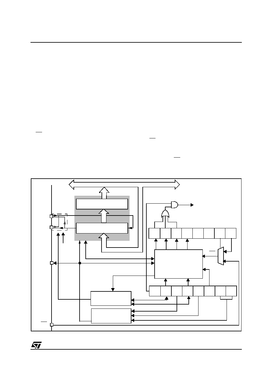
ST7LITE0, ST7SUPERLITE
57/122
11.3 SERIAL PERIPHERAL INTERFACE (SPI)
11.3.1 Introduction
The Serial Peripheral Interface (SPI) allows full-
duplex, synchronous, serial communication with
external devices. An SPI system may consist of a
master and one or more slaves however the SPI
interface can not be a master in a multi-master
system.
11.3.2 Main Features
s
Full duplex synchronous transfers (on 3 lines)
s
Simplex synchronous transfers (on 2 lines)
s
Master or slave operation
s
Six master mode frequencies (f
CPU
/4 max.)
s
f
CPU
/2 max. slave mode frequency
s
SS Management by software or hardware
s
Programmable clock polarity and phase
s
End of transfer interrupt flag
s
Write collision, Master Mode Fault and Overrun
flags
11.3.3 General Description
Figure 36
shows the serial peripheral interface
(SPI) block diagram. There are 3 registers:
≠ SPI Control Register (SPICR)
≠ SPI Control/Status Register (SPICSR)
≠ SPI Data Register (SPIDR)
The SPI is connected to external devices through
3 pins:
≠ MISO: Master In / Slave Out data
≠ MOSI: Master Out / Slave In data
≠ SCK: Serial Clock out by SPI masters and in-
put by SPI slaves
≠ SS: Slave select:
This input signal acts as a `chip select' to let
the SPI master communicate with slaves indi-
vidually and to avoid contention on the data
lines. Slave SS inputs can be driven by stand-
ard I/O ports on the master MCU.
Figure 36. Serial Peripheral Interface Block Diagram
SPIDR
Read Buffer
8-Bit Shift Register
Write
Read
Data/Address Bus
SPI
SPIE
SPE
MSTR
CPHA
SPR0
SPR1
CPOL
SERIAL CLOCK
GENERATOR
MOSI
MISO
SS
SCK
CONTROL
STATE
SPICR
SPICSR
Interrupt
request
MASTER
CONTROL
SPR2
0
7
0
7
SPIF WCOL
MODF
0
OVR
SSI
SSM
SOD
SOD
bit
SS
1
0
1
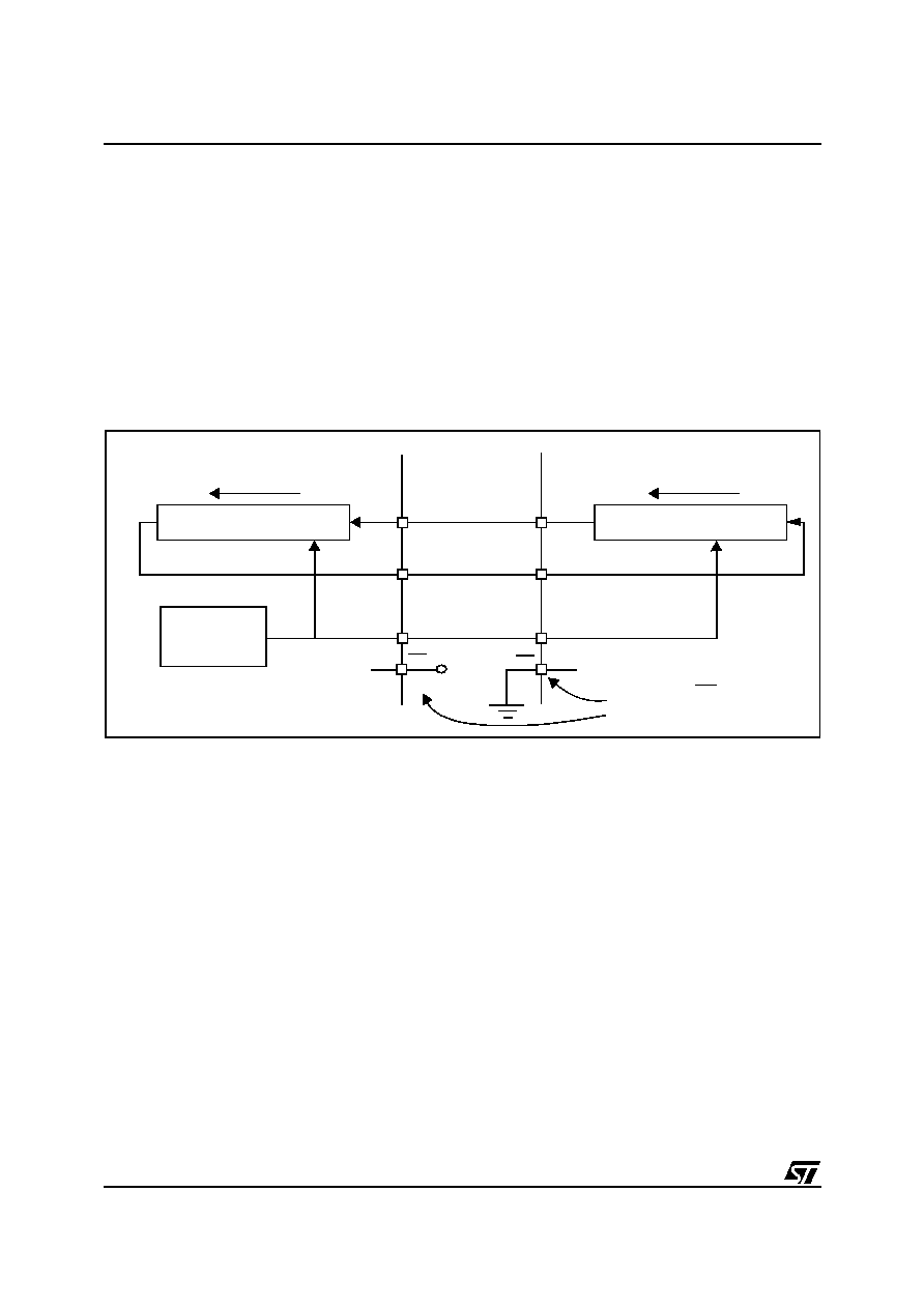
ST7LITE0, ST7SUPERLITE
58/122
SERIAL PERIPHERAL INTERFACE (Cont'd)
11.3.3.1 Functional Description
A basic example of interconnections between a
single master and a single slave is illustrated in
Figure 37
.
The MOSI pins are connected together and the
MISO pins are connected together. In this way
data is transferred serially between master and
slave (most significant bit first).
The communication is always initiated by the mas-
ter. When the master device transmits data to a
slave device via MOSI pin, the slave device re-
sponds by sending data to the master device via
the MISO pin. This implies full duplex communica-
tion with both data out and data in synchronized
with the same clock signal (which is provided by
the master device via the SCK pin).
To use a single data line, the MISO and MOSI pins
must be connected at each node ( in this case only
simplex communication is possible).
Four possible data/clock timing relationships may
be chosen (see
Figure 40
) but master and slave
must be programmed with the same timing mode.
Figure 37. Single Master/ Single Slave Application
8-BIT SHIFT REGISTER
SPI
CLOCK
GENERATOR
8-BIT SHIFT REGISTER
MISO
MOSI
MOSI
MISO
SCK
SCK
SLAVE
MASTER
SS
SS
+5V
MSBit
LSBit
MSBit
LSBit
Not used if SS is managed
by software
1
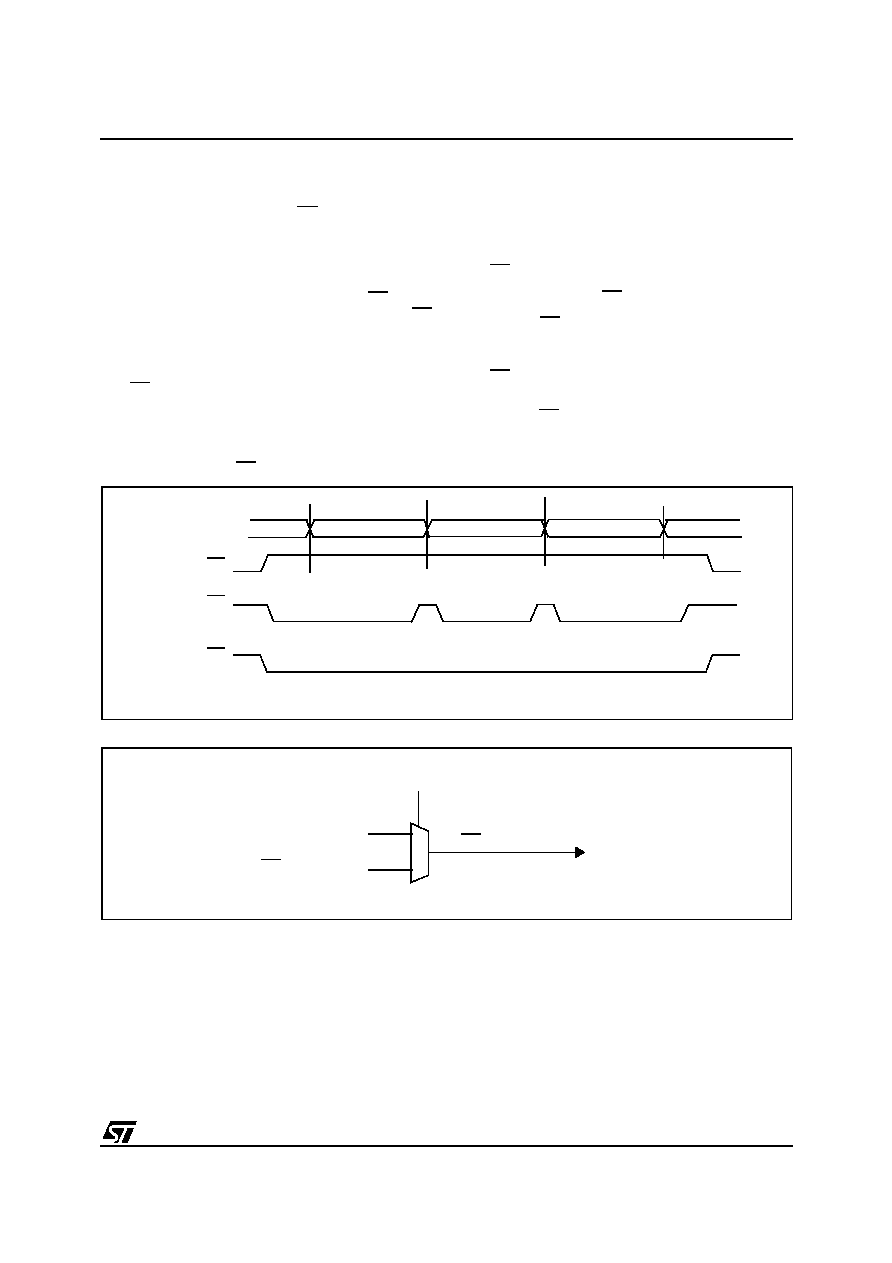
ST7LITE0, ST7SUPERLITE
59/122
SERIAL PERIPHERAL INTERFACE (Cont'd)
11.3.3.2 Slave Select Management
As an alternative to using the SS pin to control the
Slave Select signal, the application can choose to
manage the Slave Select signal by software. This
is configured by the SSM bit in the SPICSR regis-
ter (see
Figure 39
)
In software management, the external SS pin is
free for other application uses and the internal SS
signal level is driven by writing to the SSI bit in the
SPICSR register.
In Master mode:
≠ SS internal must be held high continuously
In Slave Mode:
There are two cases depending on the data/clock
timing relationship (see
Figure 38
):
If CPHA=1 (data latched on 2nd clock edge):
≠ SS internal must be held low during the entire
transmission. This implies that in single slave
applications the SS pin either can be tied to
V
SS
, or made free for standard I/O by manag-
ing the SS function by software (SSM= 1 and
SSI=0 in the in the SPICSR register)
If CPHA=0 (data latched on 1st clock edge):
≠ SS internal must be held low during byte
transmission and pulled high between each
byte to allow the slave to write to the shift reg-
ister. If SS is not pulled high, a Write Collision
error will occur when the slave writes to the
shift register (see
Section 11.3.5.3
).
Figure 38. Generic SS Timing Diagram
Figure 39. Hardware/Software Slave Select Management
MOSI/MISO
Master SS
Slave SS
(if CPHA=0)
Slave SS
(if CPHA=1)
Byte 1
Byte 2
Byte 3
1
0
SS internal
SSM bit
SSI bit
SS external pin
1

ST7LITE0, ST7SUPERLITE
60/122
SERIAL PERIPHERAL INTERFACE (Cont'd)
11.3.3.3 Master Mode Operation
In master mode, the serial clock is output on the
SCK pin. The clock frequency, polarity and phase
are configured by software (refer to the description
of the SPICSR register).
Note: The idle state of SCK must correspond to
the polarity selected in the SPICSR register (by
pulling up SCK if CPOL=1 or pulling down SCK if
CPOL=0).
To operate the SPI in master mode, perform the
following two steps in order (if the SPICSR register
is not written first, the SPICR register setting may
be not taken into account):
1. Write to the SPICSR register:
≠ Select the clock frequency by configuring the
SPR[2:0]
bits.
≠ Select the clock polarity and clock phase by
configuring the CPOL and CPHA bits.
Figure
40
shows the four possible configurations.
Note: The slave must have the same CPOL
and CPHA settings as the master.
≠ Either set the SSM bit and set the SSI bit or
clear the SSM bit and tie the SS pin high for
the complete byte transmit sequence.
2. Write to the SPICR register:
≠ Set the MSTR and SPE bits
Note: MSTR and SPE bits remain set only if
SS is high).
The transmit sequence begins when software
writes a byte in the SPIDR register.
11.3.3.4 Master Mode Transmit Sequence
When software writes to the SPIDR register, the
data byte is loaded into the 8-bit shift register and
then shifted out serially to the MOSI pin most sig-
nificant bit first.
When data transfer is complete:
≠ The SPIF bit is set by hardware
≠ An interrupt request is generated if the SPIE
bit is set and the interrupt mask in the CCR
register is cleared.
Clearing the SPIF bit is performed by the following
software sequence:
1. An access to the SPICSR register while the
SPIF bit is set
2. A read to the SPIDR register.
Note: While the SPIF bit is set, all writes to the
SPIDR register are inhibited until the SPICSR reg-
ister is read.
11.3.3.5 Slave Mode Operation
In slave mode, the serial clock is received on the
SCK pin from the master device.
To operate the SPI in slave mode:
1. Write to the SPICSR register to perform the fol-
lowing actions:
≠ Select the clock polarity and clock phase by
configuring the CPOL and CPHA bits (see
Figure 40
).
Note: The slave must have the same CPOL
and CPHA settings as the master.
≠ Manage the SS pin as described in
Section
11.3.3.2
and
Figure 38
. If CPHA=1 SS must
be held low continuously. If CPHA=0 SS must
be held low during byte transmission and
pulled up between each byte to let the slave
write in the shift register.
2. Write to the SPICR register to clear the MSTR
bit and set the SPE bit to enable the SPI I/O
functions.
11.3.3.6 Slave Mode Transmit Sequence
When software writes to the SPIDR register, the
data byte is loaded into the 8-bit shift register and
then shifted out serially to the MISO pin most sig-
nificant bit first.
The transmit sequence begins when the slave de-
vice receives the clock signal and the most signifi-
cant bit of the data on its MOSI pin.
When data transfer is complete:
≠ The SPIF bit is set by hardware
≠ An interrupt request is generated if SPIE bit is
set and interrupt mask in the CCR register is
cleared.
Clearing the SPIF bit is performed by the following
software sequence:
1. An access to the SPICSR register while the
SPIF bit is set.
2. A write or a read to the SPIDR register.
Notes: While the SPIF bit is set, all writes to the
SPIDR register are inhibited until the SPICSR reg-
ister is read.
The SPIF bit can be cleared during a second
transmission; however, it must be cleared before
the second SPIF bit in order to prevent an Overrun
condition (see
Section 11.3.5.2
).
1

ST7LITE0, ST7SUPERLITE
61/122
SERIAL PERIPHERAL INTERFACE (Cont'd)
11.3.4 Clock Phase and Clock Polarity
Four possible timing relationships may be chosen
by software, using the CPOL and CPHA bits (See
Figure 40
).
Note: The idle state of SCK must correspond to
the polarity selected in the SPICSR register (by
pulling up SCK if CPOL=1 or pulling down SCK if
CPOL=0).
The combination of the CPOL clock polarity and
CPHA (clock phase) bits selects the data capture
clock edge
Figure 40
, shows an SPI transfer with the four
combinations of the CPHA and CPOL bits. The di-
agram may be interpreted as a master or slave
timing diagram where the SCK pin, the MISO pin,
the MOSI pin are directly connected between the
master and the slave device.
Note: If CPOL is changed at the communication
byte boundaries, the SPI must be disabled by re-
setting the SPE bit.
Figure 40. Data Clock Timing Diagram
SCK
MSBit
Bit 6
Bit 5
Bit 4
Bit3
Bit 2
Bit 1
LSBit
MSBit
Bit 6
Bit 5
Bit 4
Bit3
Bit 2
Bit 1
LSBit
MISO
(from master)
MOSI
(from slave)
SS
(to slave)
CAPTURE STROBE
CPHA =1
MSBit
Bit 6
Bit 5
Bit 4
Bit3
Bit 2
Bit 1
LSBit
MSBit
Bit 6
Bit 5
Bit 4
Bit3
Bit 2
Bit 1
LSBit
MISO
(from master)
MOSI
SS
(to slave)
CAPTURE STROBE
CPHA =0
Note: This figure should not be used as a replacement for parametric information.
Refer to the Electrical Characteristics chapter.
(from slave)
(CPOL = 1)
SCK
(CPOL = 0)
SCK
(CPOL = 1)
SCK
(CPOL = 0)
1
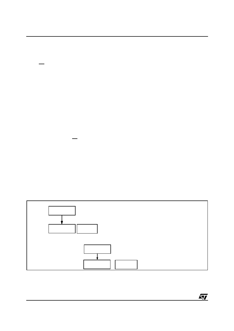
ST7LITE0, ST7SUPERLITE
62/122
SERIAL PERIPHERAL INTERFACE (Cont'd)
11.3.5 Error Flags
11.3.5.1 Master Mode Fault (MODF)
Master mode fault occurs when the master device
has its SS pin pulled low.
When a Master mode fault occurs:
≠ The MODF bit is set and an SPI interrupt re-
quest is generated if the SPIE bit is set.
≠ The SPE bit is reset. This blocks all output
from the device and disables the SPI periph-
eral.
≠ The MSTR bit is reset, thus forcing the device
into slave mode.
Clearing the MODF bit is done through a software
sequence:
1. A read access to the SPICSR register while the
MODF bit is set.
2. A write to the SPICR register.
Notes: To avoid any conflicts in an application
with multiple slaves, the SS pin must be pulled
high during the MODF bit clearing sequence. The
SPE and MSTR bits may be restored to their orig-
inal state during or after this clearing sequence.
Hardware does not allow the user to set the SPE
and MSTR bits while the MODF bit is set except in
the MODF bit clearing sequence.
11.3.5.2 Overrun Condition (OVR)
An overrun condition occurs, when the master de-
vice has sent a data byte and the slave device has
not cleared the SPIF bit issued from the previously
transmitted byte.
When an Overrun occurs:
≠ The OVR bit is set and an interrupt request is
generated if the SPIE bit is set.
In this case, the receiver buffer contains the byte
sent after the SPIF bit was last cleared. A read to
the SPIDR register returns this byte. All other
bytes are lost.
The OVR bit is cleared by reading the SPICSR
register.
11.3.5.3 Write Collision Error (WCOL)
A write collision occurs when the software tries to
write to the SPIDR register while a data transfer is
taking place with an external device. When this
happens, the transfer continues uninterrupted;
and the software write will be unsuccessful.
Write collisions can occur both in master and slave
mode. See also
Section 11.3.3.2 Slave Select
Management
.
Note: a "read collision" will never occur since the
received data byte is placed in a buffer in which
access is always synchronous with the MCU oper-
ation.
The WCOL bit in the SPICSR register is set if a
write collision occurs.
No SPI interrupt is generated when the WCOL bit
is set (the WCOL bit is a status flag only).
Clearing the WCOL bit is done through a software
sequence (see
Figure 41
).
Figure 41. Clearing the WCOL bit (Write Collision Flag) Software Sequence
Clearing sequence after SPIF = 1 (end of a data byte transfer)
1st Step
Read SPICSR
Read SPIDR
2nd Step
SPIF =0
WCOL=0
Clearing sequence before SPIF = 1 (during a data byte transfer)
1st Step
2nd Step
WCOL=0
Read SPICSR
Read SPIDR
Note: Writing to the SPIDR regis-
ter instead of reading it does not
reset the WCOL bit
RESULT
RESULT
1
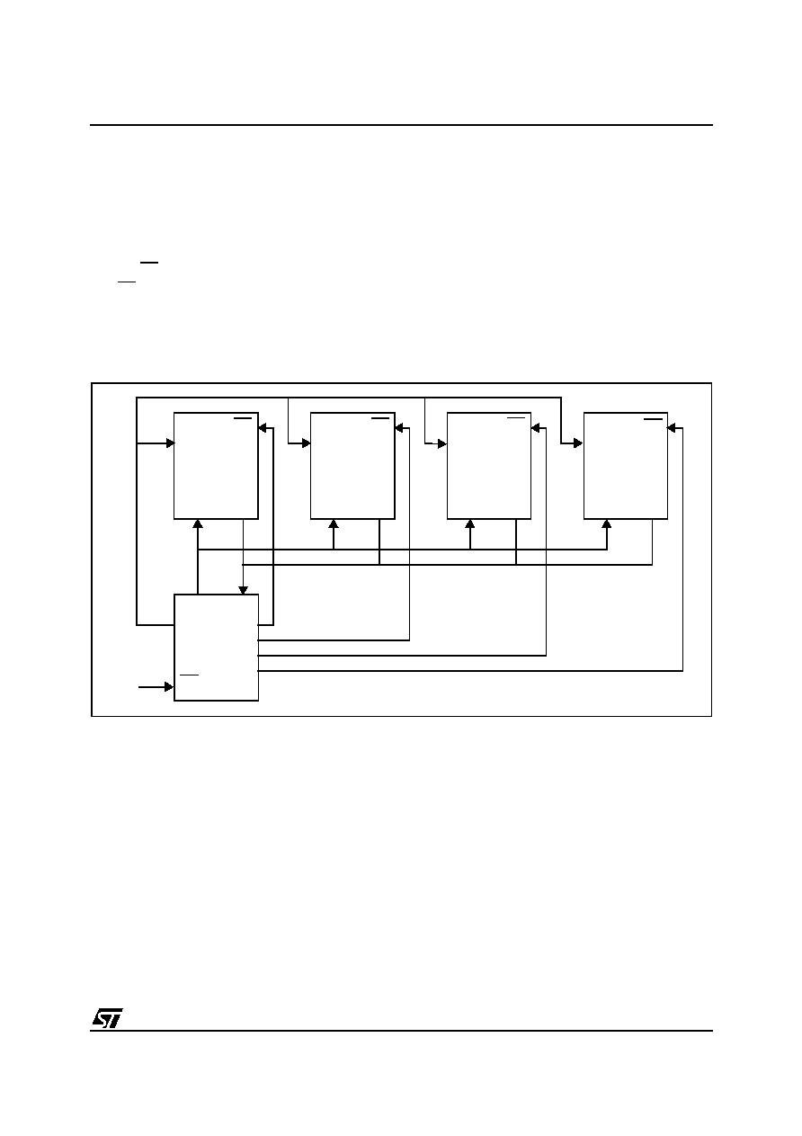
ST7LITE0, ST7SUPERLITE
63/122
SERIAL PERIPHERAL INTERFACE (Cont'd)
11.3.5.4 Single Master Systems
A typical single master system may be configured,
using an MCU as the master and four MCUs as
slaves (see
Figure 42
).
The master device selects the individual slave de-
vices by using four pins of a parallel port to control
the four SS pins of the slave devices.
The SS pins are pulled high during reset since the
master device ports will be forced to be inputs at
that time, thus disabling the slave devices.
Note: To prevent a bus conflict on the MISO line
the master allows only one active slave device
during a transmission.
For more security, the slave device may respond
to the master with the received data byte. Then the
master will receive the previous byte back from the
slave device if all MISO and MOSI pins are con-
nected and the slave has not written to its SPIDR
register.
Other transmission security methods can use
ports for handshake lines or data bytes with com-
mand fields.
Figure 42. Single Master / Multiple Slave Configuration
MISO
MOSI
MOSI
MOSI
MOSI
MOSI
MISO
MISO
MISO
MISO
SS
SS
SS
SS
SS
SCK
SCK
SCK
SCK
SCK
5V
Po
r
t
s
Slave
MCU
Slave
MCU
Slave
MCU
Slave
MCU
Master
MCU
1
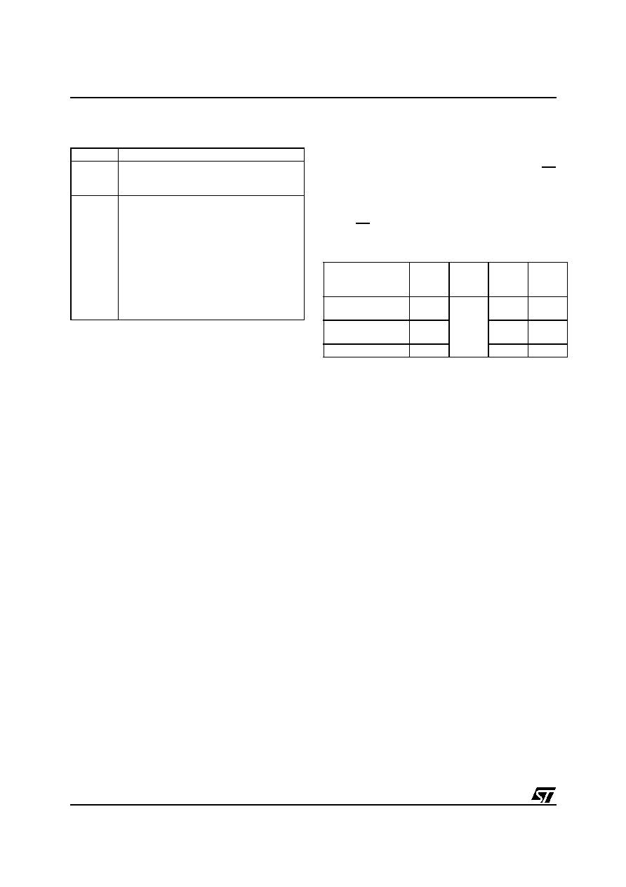
ST7LITE0, ST7SUPERLITE
64/122
SERIAL PERIPHERAL INTERFACE (Cont'd)
11.3.6 Low Power Modes
11.3.6.1 Using the SPI to wakeup the MCU from
Halt mode
In slave configuration, the SPI is able to wakeup
the ST7 device from HALT mode through a SPIF
interrupt. The data received is subsequently read
from the SPIDR register when the software is run-
ning (interrupt vector fetch). If multiple data trans-
fers have been performed before software clears
the SPIF bit, then the OVR bit is set by hardware.
Note: When waking up from Halt mode, if the SPI
remains in Slave mode, it is recommended to per-
form an extra communications cycle to bring the
SPI from Halt mode state to normal state. If the
SPI exits from Slave mode, it returns to normal
state immediately.
Caution: The SPI can wake up the ST7 from Halt
mode only if the Slave Select signal (external SS
pin or the SSI bit in the SPICSR register) is low
when the ST7 enters Halt mode. So if Slave selec-
tion is configured as external (see
Section
11.3.3.2
), make sure the master drives a low level
on the SS pin when the slave enters Halt mode.
11.3.7 Interrupts
Note: The SPI interrupt events are connected to
the same interrupt vector (see Interrupts chapter).
They generate an interrupt if the corresponding
Enable Control Bit is set and the interrupt mask in
the CC register is reset (RIM instruction).
Mode Description
WAIT
No effect on SPI.
SPI interrupt events cause the device to exit
from WAIT mode.
HALT
SPI registers are frozen.
In HALT mode, the SPI is inactive. SPI oper-
ation resumes when the MCU is woken up by
an interrupt with "exit from HALT mode" ca-
pability. The data received is subsequently
read from the SPIDR register when the soft-
ware is running (interrupt vector fetching). If
several data are received before the wake-
up event, then an overrun error is generated.
This error can be detected after the fetch of
the interrupt routine that woke up the device.
Interrupt Event
Event
Flag
Enable
Control
Bit
Exit
from
Wait
Exit
from
Halt
SPI End of Transfer
Event
SPIF
SPIE
Yes
Yes
Master Mode Fault
Event
MODF
Yes
No
Overrun Error
OVR
Yes
No
1
ST7LITE0, ST7SUPERLITE
65/122
SERIAL PERIPHERAL INTERFACE (Cont'd)
11.3.8 Register Description
CONTROL REGISTER (SPICR)
Read/Write
Reset Value: 0000 xxxx (0xh)
Bit 7 = SPIE
Serial Peripheral Interrupt Enable.
This bit is set and cleared by software.
0: Interrupt is inhibited
1: An SPI interrupt is generated whenever
SPIF=1, MODF=1 or OVR=1 in the SPICSR
register
Bit 6 = SPE
Serial Peripheral Output Enable.
This bit is set and cleared by software. It is also
cleared by hardware when, in master mode, SS=0
(see
Section 11.3.5.1 Master Mode Fault
(MODF)
). The SPE bit is cleared by reset, so the
SPI peripheral is not initially connected to the ex-
ternal pins.
0: I/O pins free for general purpose I/O
1: SPI I/O pin alternate functions enabled
Bit 5 = SPR2
Divider Enable
.
This bit is set and cleared by software and is
cleared by reset. It is used with the SPR[1:0] bits to
set the baud rate. Refer to
Table 15 SPI Master
mode SCK Frequency
.
0: Divider by 2 enabled
1: Divider by 2 disabled
Note: This bit has no effect in slave mode.
Bit 4 = MSTR
Master Mode.
This bit is set and cleared by software. It is also
cleared by hardware when, in master mode, SS=0
(see
Section 11.3.5.1 Master Mode Fault
(MODF)
).
0: Slave mode
1: Master mode. The function of the SCK pin
changes from an input to an output and the func-
tions of the MISO and MOSI pins are reversed.
Bit 3 = CPOL
Clock Polarity.
This bit is set and cleared by software. This bit de-
termines the idle state of the serial Clock. The
CPOL bit affects both the master and slave
modes.
0: SCK pin has a low level idle state
1: SCK pin has a high level idle state
Note: If CPOL is changed at the communication
byte boundaries, the SPI must be disabled by re-
setting the SPE bit.
Bit 2 = CPHA
Clock Phase.
This bit is set and cleared by software.
0: The first clock transition is the first data capture
edge.
1: The second clock transition is the first capture
edge.
Note: The slave must have the same CPOL and
CPHA settings as the master.
Bits 1:0 = SPR[1:0]
Serial Clock Frequency.
These bits are set and cleared by software. Used
with the SPR2 bit, they select the baud rate of the
SPI serial clock SCK output by the SPI in master
mode.
Note: These 2 bits have no effect in slave mode.
Table 15. SPI Master mode SCK Frequency
7
0
SPIE
SPE
SPR2
MSTR
CPOL
CPHA
SPR1
SPR0
Serial Clock
SPR2
SPR1
SPR0
f
CPU
/4
1
0
0
f
CPU
/8
0
0
0
f
CPU
/16
0
0
1
f
CPU
/32
1
1
0
f
CPU
/64
0
1
0
f
CPU
/128
0
1
1
1
ST7LITE0, ST7SUPERLITE
66/122
SERIAL PERIPHERAL INTERFACE (Cont'd)
CONTROL/STATUS REGISTER (SPICSR)
Read/Write (some bits Read Only)
Reset Value: 0000 0000 (00h)
Bit 7 = SPIF
Serial Peripheral Data Transfer Flag
(Read only).
This bit is set by hardware when a transfer has
been completed. An interrupt is generated if
SPIE=1 in the SPICR register. It is cleared by a
software sequence (an access to the SPICSR
register followed by a write or a read to the
SPIDR register).
0: Data transfer is in progress or the flag has been
cleared.
1: Data transfer between the device and an exter-
nal device has been completed.
Note: While the SPIF bit is set, all writes to the
SPIDR register are inhibited until the SPICSR reg-
ister is read.
Bit 6 = WCOL
Write Collision status (Read only).
This bit is set by hardware when a write to the
SPIDR register is done during a transmit se-
quence. It is cleared by a software sequence (see
Figure 41
).
0: No write collision occurred
1: A write collision has been detected
Bit 5 = OVR S
PI Overrun error (Read only).
This bit is set by hardware when the byte currently
being received in the shift register is ready to be
transferred into the SPIDR register while SPIF = 1
(See
Section 11.3.5.2
). An interrupt is generated if
SPIE = 1 in SPICSR register. The OVR bit is
cleared by software reading the SPICSR register.
0: No overrun error
1: Overrun error detected
Bit 4 = MODF
Mode Fault flag (Read only).
This bit is set by hardware when the SS pin is
pulled low in master mode (see
Section 11.3.5.1
Master Mode Fault (MODF)
). An SPI interrupt can
be generated if SPIE=1 in the SPICSR register.
This bit is cleared by a software sequence (An ac-
cess to the SPICSR register while MODF=1 fol-
lowed by a write to the SPICR register).
0: No master mode fault detected
1: A fault in master mode has been detected
Bit 3 = Reserved, must be kept cleared.
Bit 2 = SOD
SPI Output Disable.
This bit is set and cleared by software. When set, it
disables the alternate function of the SPI output
(MOSI in master mode / MISO in slave mode)
0: SPI output enabled (if SPE=1)
1: SPI output disabled
Bit 1 = SSM
SS Management.
This bit is set and cleared by software. When set, it
disables the alternate function of the SPI SS pin
and uses the SSI bit value instead. See
Section
11.3.3.2 Slave Select Management
.
0: Hardware management (SS managed by exter-
nal pin)
1: Software management (internal SS signal con-
trolled by SSI bit. External SS pin free for gener-
al-purpose I/O)
Bit 0 = SSI
SS Internal Mode.
This bit is set and cleared by software. It acts as a
`chip select' by controlling the level of the SS slave
select signal when the SSM bit is set.
0 : Slave selected
1 : Slave deselected
DATA I/O REGISTER (SPIDR)
Read/Write
Reset Value: Undefined
The SPIDR register is used to transmit and receive
data on the serial bus. In a master device, a write
to this register will initiate transmission/reception
of another byte.
Notes: During the last clock cycle the SPIF bit is
set, a copy of the received data byte in the shift
register is moved to a buffer. When the user reads
the serial peripheral data I/O register, the buffer is
actually being read.
While the SPIF bit is set, all writes to the SPIDR
register are inhibited until the SPICSR register is
read.
Warning: A write to the SPIDR register places
data directly into the shift register for transmission.
A read to the SPIDR register returns the value lo-
cated in the buffer and not the content of the shift
register (see
Figure 36
).
7
0
SPIF
WCOL
OVR
MODF
-
SOD
SSM
SSI
7
0
D7
D6
D5
D4
D3
D2
D1
D0
1

ST7LITE0, ST7SUPERLITE
67/122
SERIAL PERIPHERAL INTERFACE (Cont'd)
Table 16. SPI Register Map and Reset Values
Address
(Hex.)
Register
Label
7
6
5
4
3
2
1
0
31
SPIDR
Reset Value
MSB
x
x
x
x
x
x
x
LSB
x
32
SPICR
Reset Value
SPIE
0
SPE
0
SPR2
0
MSTR
0
CPOL
x
CPHA
x
SPR1
x
SPR0
x
33
SPICSR
Reset Value
SPIF
0
WCOL
0
OVR
0
MODF
0
0
SOD
0
SSM
0
SSI
0
1
ST7LITE0, ST7SUPERLITE
68/122
11.4 8-BIT A/D CONVERTER (ADC)
11.4.1 Introduction
The on-chip Analog to Digital Converter (ADC) pe-
ripheral is a 8-bit, successive approximation con-
verter with internal sample and hold circuitry. This
peripheral has up to 5 multiplexed analog input
channels (refer to device pin out description) that
allow the peripheral to convert the analog voltage
levels from up to 5 different sources.
The result of the conversion is stored in a 8-bit
Data Register. The A/D converter is controlled
through a Control/Status Register.
11.4.2 Main Features
s
8-bit conversion
s
Up to 5 channels with multiplexed input
s
Linear successive approximation
s
Dual input range
≠ 0 to V
DD
or
≠ 0V to 250mV
s
Data register (DR) which contains the results
s
Conversion complete status flag
s
On/off bit (to reduce consumption)
s
Fixed gain operational amplifier (x8) (not
available on ST7LITES5 devices)
11.4.3 Functional Description
11.4.3.1 Analog Power Supply
The block diagram is shown in
Figure 43
.
V
DD
and V
SS
are the high and low level reference
voltage pins.
Conversion accuracy may therefore be impacted
by voltage drops and noise in the event of heavily
loaded or badly decoupled power supply lines.
For more details, refer to the Electrical character-
istics section.
11.4.3.2 Input Voltage Amplifier
The input voltage can be amplified by a factor of 8
by enabling the AMPSEL bit in the ADAMP regis-
ter.
When the amplifier is enabled, the input range is
0V to 250 mV.
For example, if V
DD
= 5V, then the ADC can con-
vert voltages in the range 0V to 250mV with an
ideal resolution of 2.4mV (equivalent to 11-bit res-
olution with reference to a V
SS
to V
DD
range).
For more details, refer to the Electrical character-
istics section.
Note: The amplifier is switched on by the ADON
bit in the ADCCSR register, so no additional start-
up time is required when the amplifier is selected
by the AMPSEL bit.
Figure 43. ADC Block Diagram
CH2
CH1
0
EOC SPEED ADON
0
CH0
ADCCSR
AIN0
AIN1
ANALOG TO DIGITAL
CONVERTER
AINx
ANALOG
MUX
R
ADC
C
ADC
D2
D1
D3
D7
D6
D5
D4
D0
ADCDR
3
f
ADC
HOLD CONTROL
x 1 or
x 8
AMPSEL bit
(ADCAMP Register)
f
CPU
0
1
1
0
DIV 2
DIV 4
SLOW
bit
(ADCAMP Register)
7
0
1
ST7LITE0, ST7SUPERLITE
69/122
8-BIT A/D CONVERTER (ADC) (Cont'd)
11.4.3.3 Digital A/D Conversion Result
The conversion is monotonic, meaning that the re-
sult never decreases if the analog input does not
and never increases if the analog input does not.
If the input voltage (V
AIN
) is greater than or equal
to V
DDA
(high-level voltage reference) then the
conversion result in the DR register is FFh (full
scale) without overflow indication.
If input voltage (V
AIN
) is lower than or equal to
V
SSA
(low-level voltage reference) then the con-
version result in the DR register is 00h.
The A/D converter is linear and the digital result of
the conversion is stored in the ADCDR register.
The accuracy of the conversion is described in the
parametric section.
R
AIN
is the maximum recommended impedance
for an analog input signal. If the impedance is too
high, this will result in a loss of accuracy due to
leakage and sampling not being completed in the
alloted time.
11.4.3.4 A/D Conversion Phases
The A/D conversion is based on two conversion
phases as shown in
Figure 44
:
s
Sample capacitor loading [duration: t
SAMPLE
]
During this phase, the V
AIN
input voltage to be
measured is loaded into the C
ADC
sample
capacitor.
s
A/D conversion [duration: t
HOLD
]
During this phase, the A/D conversion is
computed (8 successive approximations cycles)
and the C
ADC
sample capacitor is disconnected
from the analog input pin to get the optimum
analog to digital conversion accuracy.
s
The total conversion time:
t
CONV =
t
SAMPLE
+ t
HOLD
While the ADC is on, these two phases are contin-
uously repeated.
At the end of each conversion, the sample capaci-
tor is kept loaded with the previous measurement
load. The advantage of this behaviour is that it
minimizes the current consumption on the analog
pin in case of single input channel measurement.
11.4.3.5 Software Procedure
Refer to the control/status register (CSR) and data
register (DR) in
Section 11.4.6
for the bit defini-
tions and to
Figure 44
for the timings.
ADC Configuration
The analog input ports must be configured as in-
put, no pull-up, no interrupt. Refer to the ´I/O
portsª chapter. Using these pins as analog inputs
does not affect the ability of the port to be read as
a logic input.
In the CSR register:
≠ Select the CH[2:0] bits to assign the analog
channel to be converted.
ADC Conversion
In the CSR register:
≠ Set the ADON bit to enable the A/D converter
and to start the first conversion. From this time
on, the ADC performs a continuous conver-
sion of the selected channel.
When a conversion is complete
≠ The EOC bit is set by hardware.
≠ No interrupt is generated.
≠ The result is in the DR register and remains
valid until the next conversion has ended.
A write to the ADCCSR register (with ADON set)
aborts the current conversion, resets the EOC bit
and starts a new conversion.
Figure 44. ADC Conversion Timings
11.4.4 Low Power Modes
Note: The A/D converter may be disabled by reset-
ting the ADON bit. This feature allows reduced
power consumption when no conversion is needed
and between single shot conversions.
11.4.5 Interrupts
None
Mode Description
WAIT
No effect on A/D Converter
HALT
A/D Converter disabled.
After wakeup from Halt mode, the A/D Con-
verter requires a stabilization time before ac-
curate conversions can be performed.
ADCCSR WRITE
ADON
EOC BIT SET
t
SAMPLE
t
HOLD
OPERATION
HOLD
CONTROL
t
CONV
1

ST7LITE0, ST7SUPERLITE
70/122
8-BIT A/D CONVERTER (ADC) (Cont'd)
11.4.6 Register Description
CONTROL/STATUS REGISTER (ADCCSR)
Read /Write
Reset Value: 0000 0000 (00h)
Bit 7 = EOC
Conversion Complete
This bit is set by hardware. It is cleared by soft-
ware reading the result in the DR register or writing
to the CSR register.
0: Conversion is not complete
1: Conversion can be read from the DR register
Bit 6 = SPEED
ADC clock selection
This bit is set and cleared by software. It is used
together with the SLOW bit to configure the ADC
clock speed. Refer to the table in the SLOW bit de-
scription.
Bit 5 = ADON
A/D Converter and Amplifier On
This bit is set and cleared by software.
0: A/D converter and amplifier are switched off
1: A/D converter and amplifier are switched on
Note: Amplifier not available on ST7LITES5
devices
Bit 4:3 = Reserved.
must always be cleared.
Bits 2:0 = CH[2:0]
Channel Selection
These bits are set and cleared by software. They
select the analog input to convert.
Notes:
1. The number of pins AND the channel selection
varies according to the device. Refer to the device
pinout.
2. A write to the ADCCSR register (with ADON set)
aborts the current conversion, resets the EOC bit
and starts a new conversion.
DATA REGISTER (ADCDAT)
Read Only
Reset Value: 0000 0000 (00h)
Bits 7:0 = D[7:0]
Analog Converted Value
This register contains the converted analog value
in the range 00h to FFh.
Note: Reading this register reset the EOC flag.
AMPLIFIER CONTROL REGISTER (ADCAMP)
Read/Write
Reset Value: 0000 0000 (00h)
Bit 7:4 = Reserved. Forced by hardware to 0.
Bit 3 = SLOW
Slow mode
This bit is set and cleared by software. It is used
together with the SPEED bit to configure the ADC
clock speed as shown on the table below.
Bit 2 = AMPSEL
Amplifier Selection Bit
This bit is set and cleared by software. For
ST7LITES5 devices, this bit must be kept at its re-
set value (0).
0: Amplifier is not selected
1: Amplifier is selected
Note: When AMPSEL=1 it is mandatory that f
ADC
be less than or equal to 2 MHz.
Bit 1:0 = Reserved. Forced by hardware to 0.
Note: If ADC settings are changed by writing the
ADCAMP register while the ADC is running, a
dummy conversion is needed before obtaining re-
sults with the new settings.
7
0
EOC
SPEED ADON
0
0
CH2
CH1
CH0
Channel Pin
1
CH2
CH1
CH0
AIN0
0
0
0
AIN1
0
0
1
AIN2
0
1
0
AIN3
0
1
1
AIN4
1
0
0
7
0
D7
D6
D5
D4
D3
D2
D1
D0
7
0
0
0
0
0
SLOW
AMP-
SEL
0
0
f
ADC
SLOW SPEED
f
CPU
/2
0
0
f
CPU
0
1
f
CPU
/4
1
x
1

ST7LITE0, ST7SUPERLITE
71/122
Table 17. ADC Register Map and Reset Values
Address
(Hex.)
Register
Label
7
6
5
4
3
2
1
0
34h
ADCCSR
Reset Value
EOC
0
SPEED
0
ADON
0
0
0
CH2
0
CH1
0
CH0
0
35h
ADCDAT
Reset Value
D7
0
D6
0
D5
0
D4
0
D3
0
D2
0
D1
0
D0
0
36h
ADCAMP
Reset Value
0
0
0
0
SLOW
0
AMPSEL
0
0
0
1
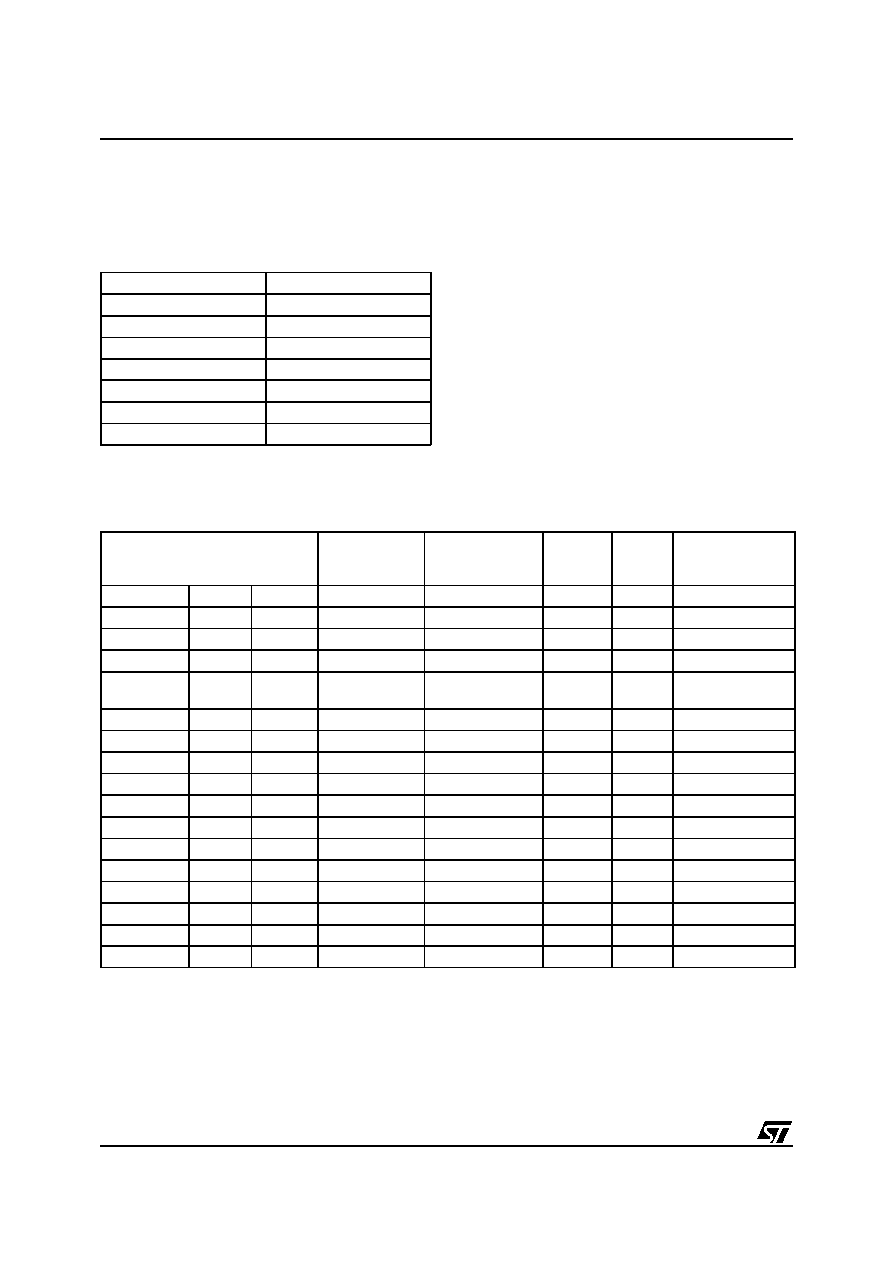
ST7LITE0, ST7SUPERLITE
72/122
12 INSTRUCTION SET
12.1 ST7 ADDRESSING MODES
The ST7 Core features 17 different addressing
modes which can be classified in 7 main groups:
The ST7 Instruction set is designed to minimize
the number of bytes required per instruction: To do
so, most of the addressing modes may be subdi-
vided in two sub-modes called long and short:
≠ Long addressing mode is more powerful be-
cause it can use the full 64 Kbyte address space,
however it uses more bytes and more CPU cy-
cles.
≠ Short addressing mode is less powerful because
it can generally only access page zero (0000h -
00FFh range), but the instruction size is more
compact, and faster. All memory to memory in-
structions use short addressing modes only
(CLR, CPL, NEG, BSET, BRES, BTJT, BTJF,
INC, DEC, RLC, RRC, SLL, SRL, SRA, SWAP)
The ST7 Assembler optimizes the use of long and
short addressing modes.
Table 18. ST7 Addressing Mode Overview
Note 1. At the time the instruction is executed, the Program Counter (PC) points to the instruction follow-
ing JRxx.
Addressing Mode
Example
Inherent
nop
Immediate
ld A,#$55
Direct
ld A,$55
Indexed
ld A,($55,X)
Indirect
ld A,([$55],X)
Relative
jrne loop
Bit operation
bset byte,#5
Mode
Syntax
Destination/
Source
Pointer
Address
(Hex.)
Pointer
Size
(Hex.)
Length
(Bytes)
Inherent
nop
+ 0
Immediate
ld A,#$55
+ 1
Short
Direct
ld A,$10
00..FF
+ 1
Long
Direct
ld A,$1000
0000..FFFF
+ 2
No Offset
Direct
Indexed
ld A,(X)
00..FF
+ 0 (with X register)
+ 1 (with Y register)
Short
Direct
Indexed
ld A,($10,X)
00..1FE
+ 1
Long
Direct
Indexed
ld A,($1000,X)
0000..FFFF
+ 2
Short
Indirect
ld A,[$10]
00..FF
00..FF
byte
+ 2
Long
Indirect
ld A,[$10.w]
0000..FFFF
00..FF
word
+ 2
Short
Indirect
Indexed
ld A,([$10],X)
00..1FE
00..FF
byte
+ 2
Long
Indirect
Indexed
ld A,([$10.w],X)
0000..FFFF
00..FF
word
+ 2
Relative
Direct
jrne loop
PC-128/PC+127
1)
+ 1
Relative
Indirect
jrne [$10]
PC-128/PC+127
1)
00..FF
byte
+ 2
Bit
Direct
bset $10,#7
00..FF
+ 1
Bit
Indirect
bset [$10],#7
00..FF
00..FF
byte
+ 2
Bit
Direct
Relative
btjt $10,#7,skip
00..FF
+ 2
Bit
Indirect
Relative
btjt [$10],#7,skip 00..FF
00..FF
byte
+ 3
1
ST7LITE0, ST7SUPERLITE
73/122
ST7 ADDRESSING MODES (Cont'd)
12.1.1 Inherent
All Inherent instructions consist of a single byte.
The opcode fully specifies all the required informa-
tion for the CPU to process the operation.
12.1.2 Immediate
Immediate instructions have two bytes, the first
byte contains the opcode, the second byte con-
tains the operand value.
12.1.3 Direct
In Direct instructions, the operands are referenced
by their memory address.
The direct addressing mode consists of two sub-
modes:
Direct (short)
The address is a byte, thus requires only one byte
after the opcode, but only allows 00 - FF address-
ing space.
Direct (long)
The address is a word, thus allowing 64 Kbyte ad-
dressing space, but requires 2 bytes after the op-
code.
12.1.4 Indexed (No Offset, Short, Long)
In this mode, the operand is referenced by its
memory address, which is defined by the unsigned
addition of an index register (X or Y) with an offset.
The indirect addressing mode consists of three
sub-modes:
Indexed (No Offset)
There is no offset, (no extra byte after the opcode),
and allows 00 - FF addressing space.
Indexed (Short)
The offset is a byte, thus requires only one byte af-
ter the opcode and allows 00 - 1FE addressing
space.
Indexed (long)
The offset is a word, thus allowing 64 Kbyte ad-
dressing space and requires 2 bytes after the op-
code.
12.1.5 Indirect (Short, Long)
The required data byte to do the operation is found
by its memory address, located in memory (point-
er).
The pointer address follows the opcode. The indi-
rect addressing mode consists of two sub-modes:
Indirect (short)
The pointer address is a byte, the pointer size is a
byte, thus allowing 00 - FF addressing space, and
requires 1 byte after the opcode.
Indirect (long)
The pointer address is a byte, the pointer size is a
word, thus allowing 64 Kbyte addressing space,
and requires 1 byte after the opcode.
Inherent Instruction
Function
NOP
No operation
TRAP
S/W Interrupt
WFI
Wait For Interrupt (Low Power
Mode)
HALT
Halt Oscillator (Lowest Power
Mode)
RET
Sub-routine Return
IRET
Interrupt Sub-routine Return
SIM
Set Interrupt Mask
RIM
Reset Interrupt Mask
SCF
Set Carry Flag
RCF
Reset Carry Flag
RSP
Reset Stack Pointer
LD
Load
CLR
Clear
PUSH/POP
Push/Pop to/from the stack
INC/DEC
Increment/Decrement
TNZ
Test Negative or Zero
CPL, NEG
1 or 2 Complement
MUL
Byte Multiplication
SLL, SRL, SRA, RLC,
RRC
Shift and Rotate Operations
SWAP
Swap Nibbles
Immediate Instruction
Function
LD
Load
CP
Compare
BCP
Bit Compare
AND, OR, XOR
Logical Operations
ADC, ADD, SUB, SBC
Arithmetic Operations
1
ST7LITE0, ST7SUPERLITE
74/122
ST7 ADDRESSING MODES (Cont'd)
12.1.6 Indirect Indexed (Short, Long)
This is a combination of indirect and short indexed
addressing modes. The operand is referenced by
its memory address, which is defined by the un-
signed addition of an index register value (X or Y)
with a pointer value located in memory. The point-
er address follows the opcode.
The indirect indexed addressing mode consists of
two sub-modes:
Indirect Indexed (Short)
The pointer address is a byte, the pointer size is a
byte, thus allowing 00 - 1FE addressing space,
and requires 1 byte after the opcode.
Indirect Indexed (Long)
The pointer address is a byte, the pointer size is a
word, thus allowing 64 Kbyte addressing space,
and requires 1 byte after the opcode.
Table 19. Instructions Supporting Direct,
Indexed, Indirect and Indirect Indexed
Addressing Modes
12.1.7 Relative Mode (Direct, Indirect)
This addressing mode is used to modify the PC
register value by adding an 8-bit signed offset to it.
The relative addressing mode consists of two sub-
modes:
Relative (Direct)
The offset follows the opcode.
Relative (Indirect)
The offset is defined in memory, of which the ad-
dress follows the opcode.
Long and Short
Instructions
Function
LD
Load
CP
Compare
AND, OR, XOR
Logical Operations
ADC, ADD, SUB, SBC
Arithmetic Addition/subtrac-
tion operations
BCP
Bit Compare
Short Instructions Only
Function
CLR
Clear
INC, DEC
Increment/Decrement
TNZ
Test Negative or Zero
CPL, NEG
1 or 2 Complement
BSET, BRES
Bit Operations
BTJT, BTJF
Bit Test and Jump Opera-
tions
SLL, SRL, SRA, RLC,
RRC
Shift and Rotate Operations
SWAP
Swap Nibbles
CALL, JP
Call or Jump subroutine
Available Relative Direct/
Indirect Instructions
Function
JRxx
Conditional Jump
CALLR
Call Relative
1
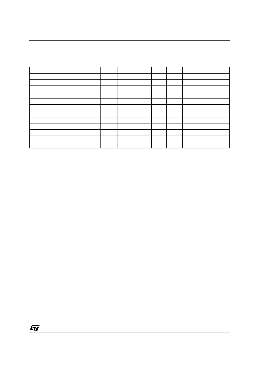
ST7LITE0, ST7SUPERLITE
75/122
12.2 INSTRUCTION GROUPS
The ST7 family devices use an Instruction Set
consisting of 63 instructions. The instructions may
be subdivided into 13 main groups as illustrated in
the following table:
Using a pre-byte
The instructions are described with one to four
bytes.
In order to extend the number of available op-
codes for an 8-bit CPU (256 opcodes), three differ-
ent prebyte opcodes are defined. These prebytes
modify the meaning of the instruction they pre-
cede.
The whole instruction becomes:
PC-2 End of previous instruction
PC-1 Prebyte
PC
Opcode
PC+1 Additional word (0 to 2) according to the
number of bytes required to compute the
effective address
These prebytes enable instruction in Y as well as
indirect addressing modes to be implemented.
They precede the opcode of the instruction in X or
the instruction using direct addressing mode. The
prebytes are:
PDY 90 Replace an X based instruction using
immediate, direct, indexed, or inherent
addressing mode by a Y one.
PIX 92
Replace an instruction using direct, di-
rect bit, or direct relative addressing
mode to an instruction using the corre-
sponding indirect addressing mode.
It also changes an instruction using X
indexed addressing mode to an instruc-
tion using indirect X indexed addressing
mode.
PIY 91
Replace an instruction using X indirect
indexed addressing mode by a Y one.
Load and Transfer
LD
CLR
Stack operation
PUSH
POP
RSP
Increment/Decrement
INC
DEC
Compare and Tests
CP
TNZ
BCP
Logical operations
AND
OR
XOR
CPL
NEG
Bit Operation
BSET
BRES
Conditional Bit Test and Branch
BTJT
BTJF
Arithmetic operations
ADC
ADD
SUB
SBC
MUL
Shift and Rotates
SLL
SRL
SRA
RLC
RRC
SWAP
SLA
Unconditional Jump or Call
JRA
JRT
JRF
JP
CALL
CALLR
NOP
RET
Conditional Branch
JRxx
Interruption management
TRAP
WFI
HALT
IRET
Condition Code Flag modification
SIM
RIM
SCF
RCF
1
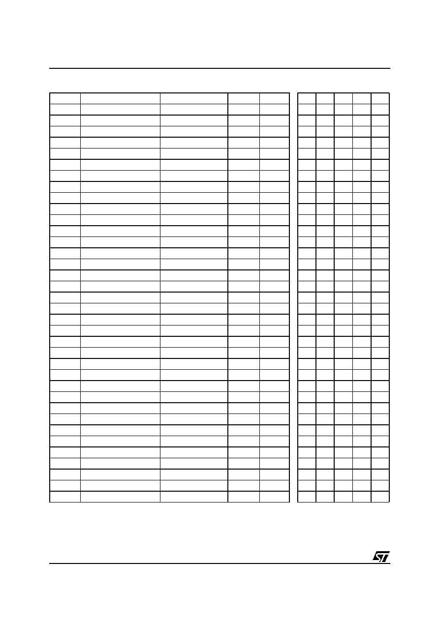
ST7LITE0, ST7SUPERLITE
76/122
INSTRUCTION GROUPS (Cont'd)
Mnemo
Description
Function/Example
Dst
Src
H
I
N
Z
C
ADC
Add with Carry
A = A + M + C
A
M
H
N
Z
C
ADD
Addition
A = A + M
A
M
H
N
Z
C
AND
Logical And
A = A . M
A
M
N
Z
BCP
Bit compare A, Memory
tst (A . M)
A
M
N
Z
BRES
Bit Reset
bres Byte, #3
M
BSET
Bit Set
bset Byte, #3
M
BTJF
Jump if bit is false (0)
btjf Byte, #3, Jmp1
M
C
BTJT
Jump if bit is true (1)
btjt Byte, #3, Jmp1
M
C
CALL
Call subroutine
CALLR
Call subroutine relative
CLR
Clear
reg, M
0
1
CP
Arithmetic Compare
tst(Reg - M)
reg
M
N
Z
C
CPL
One Complement
A = FFH-A
reg, M
N
Z
1
DEC
Decrement
dec Y
reg, M
N
Z
HALT
Halt
0
IRET
Interrupt routine return
Pop CC, A, X, PC
H
I
N
Z
C
INC
Increment
inc X
reg, M
N
Z
JP
Absolute Jump
jp [TBL.w]
JRA
Jump relative always
JRT
Jump relative
JRF
Never jump
jrf *
JRIH
Jump if ext. interrupt = 1
JRIL
Jump if ext. interrupt = 0
JRH
Jump if H = 1
H = 1 ?
JRNH
Jump if H = 0
H = 0 ?
JRM
Jump if I = 1
I = 1 ?
JRNM
Jump if I = 0
I = 0 ?
JRMI
Jump if N = 1 (minus)
N = 1 ?
JRPL
Jump if N = 0 (plus)
N = 0 ?
JREQ
Jump if Z = 1 (equal)
Z = 1 ?
JRNE
Jump if Z = 0 (not equal)
Z = 0 ?
JRC
Jump if C = 1
C = 1 ?
JRNC
Jump if C = 0
C = 0 ?
JRULT
Jump if C = 1
Unsigned <
JRUGE
Jump if C = 0
Jmp if unsigned >=
JRUGT
Jump if (C + Z = 0)
Unsigned >
1
ST7LITE0, ST7SUPERLITE
77/122
INSTRUCTION GROUPS (Cont'd)
Mnemo
Description
Function/Example
Dst
Src
H
I
N
Z
C
JRULE
Jump if (C + Z = 1)
Unsigned <=
LD
Load
dst <= src
reg, M
M, reg
N
Z
MUL
Multiply
X,A = X * A
A, X, Y
X, Y, A
0
0
NEG
Negate (2's compl)
neg $10
reg, M
N
Z
C
NOP
No Operation
OR
OR operation
A = A + M
A
M
N
Z
POP
Pop from the Stack
pop reg
reg
M
pop CC
CC
M
H
I
N
Z
C
PUSH
Push onto the Stack
push Y
M
reg, CC
RCF
Reset carry flag
C = 0
0
RET
Subroutine Return
RIM
Enable Interrupts
I = 0
0
RLC
Rotate left true C
C <= Dst <= C
reg, M
N
Z
C
RRC
Rotate right true C
C => Dst => C
reg, M
N
Z
C
RSP
Reset Stack Pointer
S = Max allowed
SBC
Subtract with Carry
A = A - M - C
A
M
N
Z
C
SCF
Set carry flag
C = 1
1
SIM
Disable Interrupts
I = 1
1
SLA
Shift left Arithmetic
C <= Dst <= 0
reg, M
N
Z
C
SLL
Shift left Logic
C <= Dst <= 0
reg, M
N
Z
C
SRL
Shift right Logic
0 => Dst => C
reg, M
0
Z
C
SRA
Shift right Arithmetic
Dst7 => Dst => C
reg, M
N
Z
C
SUB
Subtraction
A = A - M
A
M
N
Z
C
SWAP
SWAP nibbles
Dst[7..4] <=> Dst[3..0] reg, M
N
Z
TNZ
Test for Neg & Zero
tnz lbl1
N
Z
TRAP
S/W trap
S/W interrupt
1
WFI
Wait for Interrupt
0
XOR
Exclusive OR
A = A XOR M
A
M
N
Z
1
ST7LITE0, ST7SUPERLITE
78/122
13 ELECTRICAL CHARACTERISTICS
13.1 PARAMETER CONDITIONS
Unless otherwise specified, all voltages are re-
ferred to V
SS
.
13.1.1 Minimum and Maximum values
Unless otherwise specified the minimum and max-
imum values are guaranteed in the worst condi-
tions of ambient temperature, supply voltage and
frequencies by tests in production on 100% of the
devices with an ambient temperature at T
A
=25∞C
and T
A
=T
A
max (given by the selected temperature
range).
Data based on characterization results, design
simulation and/or technology characteristics are
indicated in the table footnotes and are not tested
in production. Based on characterization, the min-
imum and maximum values refer to sample tests
and represent the mean value plus or minus three
times the standard deviation (mean±3
).
13.1.2 Typical values
Unless otherwise specified, typical data are based
on T
A
=25∞C, V
DD
=5V (for the 4.5V
V
DD
5.5V
voltage range), V
DD
=3.75V (for the 3V
V
DD
4.5V
voltage range) and V
DD
=2.7V (for the
2.4V
V
DD
3V voltage range). They are given only
as design guidelines and are not tested.
13.1.3 Typical curves
Unless otherwise specified, all typical curves are
given only as design guidelines and are not tested.
13.1.4 Loading capacitor
The loading conditions used for pin parameter
measurement are shown in
Figure 45
.
Figure 45. Pin loading conditions
13.1.5 Pin input voltage
The input voltage measurement on a pin of the de-
vice is described in
Figure 46
.
Figure 46. Pin input voltage
C
L
ST7 PIN
V
IN
ST7 PIN
1
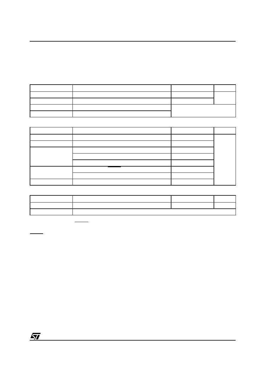
ST7LITE0, ST7SUPERLITE
79/122
13.2 ABSOLUTE MAXIMUM RATINGS
Stresses above those listed as "absolute maxi-
mum ratings" may cause permanent damage to
the device. This is a stress rating only and func-
tional operation of the device under these condi-
tions is not implied. Exposure to maximum rating
conditions for extended periods may affect device
reliability.
13.2.1 Voltage Characteristics
13.2.2 Current Characteristics
13.2.3 Thermal Characteristics
Notes:
1. Directly connecting the RESET and I/O pins to V
DD
or V
SS
could damage the device if an unintentional internal reset
is generated or an unexpected change of the I/O configuration occurs (for example, due to a corrupted program counter).
To guarantee safe operation, this connection has to be done through a pull-up or pull-down resistor (typical: 4.7k
for
RESET, 10k
for I/Os). Unused I/O pins must be tied in the same way to V
DD
or V
SS
according to their reset configuration.
2. When the current limitation is not possible, the V
IN
absolute maximum rating must be respected, otherwise refer to
I
INJ(PIN)
specification. A positive injection is induced by V
IN
>V
DD
while a negative injection is induced by V
IN
<V
SS
.
3. All power (V
DD
) and ground (V
SS
) lines must always be connected to the external supply.
4. Negative injection disturbs the analog performance of the device. In particular, it induces leakage currents throughout
the device including the analog inputs. To avoid undesirable effects on the analog functions, care must be taken:
- Analog input pins must have a negative injection less than 0.8 mA (assuming that the impedance of the analog voltage
is lower than the specified limits)
- Pure digital pins must have a negative injection less than 1.6mA. In addition, it is recommended to inject the current as
far as possible from the analog input pins.
5. When several inputs are submitted to a current injection, the maximum
I
INJ(PIN)
is the absolute sum of the positive
and negative injected currents (instantaneous values). These results are based on characterisation with
I
INJ(PIN)
maxi-
mum current injection on four I/O port pins of the device.
6. True open drain I/O port pins do not accept positive injection.
Symbol
Ratings
Maximum value
Unit
V
DD
- V
SS
Supply voltage
7.0
V
V
IN
Input voltage on any pin
1) & 2)
V
SS
-0.3 to V
DD
+0.3
V
ESD(HBM)
Electrostatic discharge voltage (Human Body Model)
see
section 13.7.2 on page 91
V
ESD(MM)
Electrostatic discharge voltage (Machine Model)
Symbol
Ratings
Maximum value
Unit
I
VDD
Total current into V
DD
power lines (source)
3)
100
mA
I
VSS
Total current out of V
SS
ground lines (sink)
3)
100
I
IO
Output current sunk by any standard I/O and control pin
25
Output current sunk by any high sink I/O pin
50
Output current source by any I/Os and control pin
- 25
I
INJ(PIN)
2) & 4)
Injected current on RESET pin
± 5
Injected current on any other pin
5) & 6)
± 5
I
INJ(PIN)
2)
Total injected current (sum of all I/O and control pins)
5)
± 20
Symbol
Ratings
Value
Unit
T
STG
Storage temperature range
-65 to +150
∞C
T
J
Maximum junction temperature (see
Section 14.2 THERMAL CHARACTERISTICS
)
1
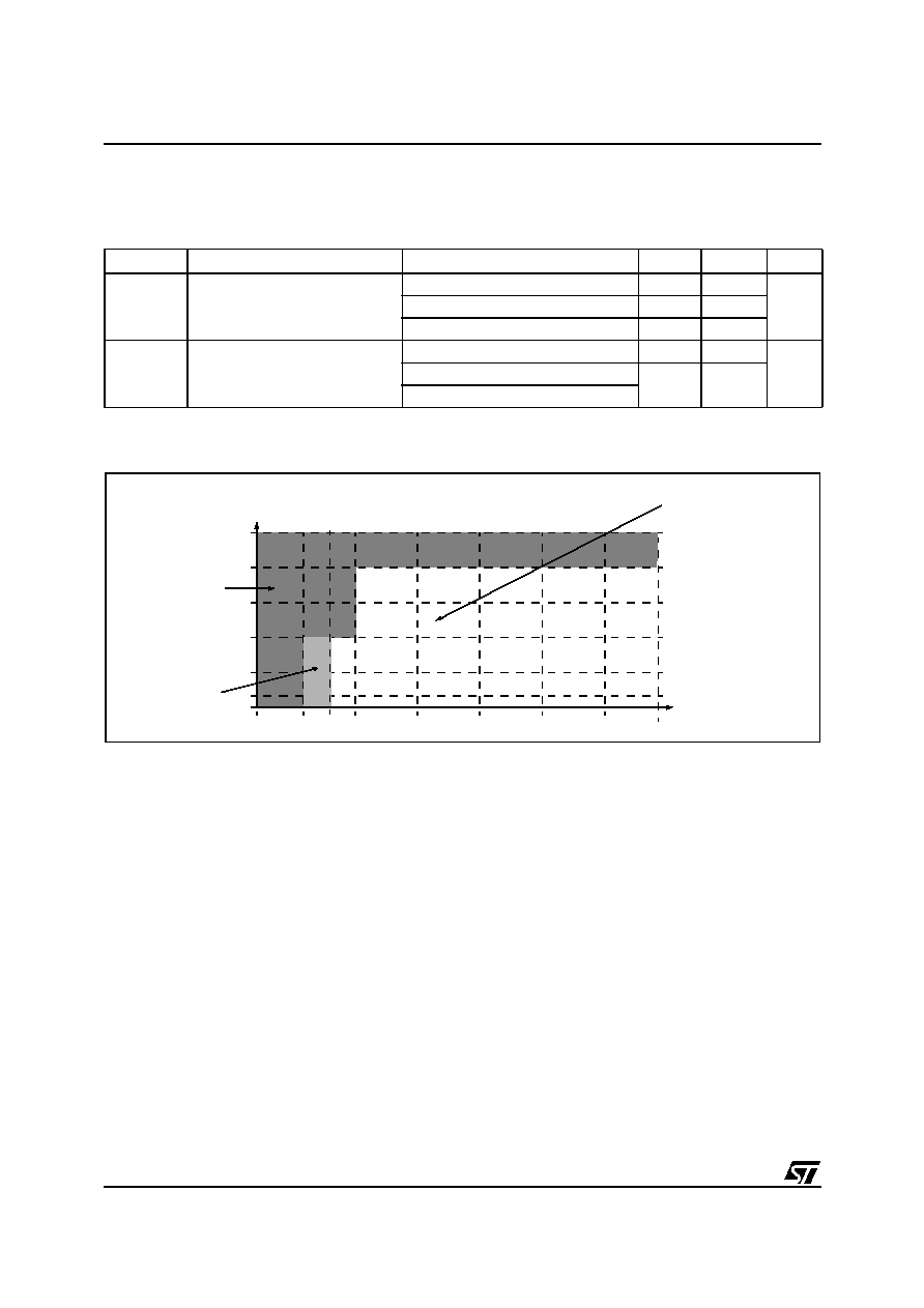
ST7LITE0, ST7SUPERLITE
80/122
13.3 OPERATING CONDITIONS
13.3.1 General Operating Conditions: Suffix 6 Devices
T
A
= -40 to +85∞C unless otherwise specified.
Figure 47. f
CLKIN
Maximum Operating Frequency Versus V
DD
Supply Voltage
Symbol
Parameter
Conditions
Min
Max
Unit
V
DD
Supply voltage
f
OSC
= 8 MHz. max., T
A
=
0 to 70∞C
2.4
5.5
V
f
OSC
= 8 MHz. max.
2.7
5.5
f
OSC
= 16 MHz. max.
3.3
5.5
f
CLKIN
External clock frequency on
CLKIN pin
V
DD
3.3V
0
16
MHz
V
DD
2.4V, T
A
=
0 to +70∞C
0
8
V
DD
2.7V
f
CLKIN
[MHz]
SUPPLY VOLTAGE [V]
16
8
4
1
0
2.0
2.4
3.3
3.5
4.0
4.5
5.0
FUNCTIONALITY
NOT GUARANTEED
IN THIS AREA
5.5
FUNCTIONALITY
GUARANTEED
IN THIS AREA
(UNLESS OTHERWISE
STATED IN THE
TABLES OF
PARAMETRIC DATA)
2.7
FUNCTIONALITY
GUARANTEED
IN THIS AREA
AT T
A
0 to 70∞C
1

ST7LITE0, ST7SUPERLITE
81/122
13.3.2 Operating Conditions with Low Voltage Detector (LVD)
T
A
= -40 to 125∞C, unless otherwise specified
Notes:
1. Not tested in production. The V
DD
rise time rate condition is needed to ensure a correct device power-on and LVD reset.
When the V
DD
slope is outside these values, the LVD may not ensure a proper reset of the MCU.
13.3.3 Auxiliary Voltage Detector (AVD) Thresholds
T
A
= -40 to 125∞C, unless otherwise specified
13.3.4 Internal RC Oscillator and PLL
The ST7 internal clock can be supplied by an internal RC oscillator and PLL (selectable by option byte).
Symbol
Parameter
Conditions
Min Typ
Max Unit
V
IT+
(LVD)
Reset release threshold
(V
DD
rise)
High Threshold
Med. Threshold
Low Threshold
4.00
3.40
2.65
4.25
3.60
2.90
4.50
3.80
3.15
V
V
IT-
(LVD)
Reset generation threshold
(V
DD
fall)
High Threshold
Med. Threshold
Low Threshold
3.80
3.20
2.40
4.05
3.40
2.70
4.30
3.65
2.90
V
hys
LVD voltage threshold hysteresis
V
IT+
(LVD)
-V
IT-
(LVD)
200
mV
Vt
POR
V
DD
rise time rate
1)
20
20000
µ
s/V
t
g(VDD)
Filtered glitch delay on V
DD
Not detected by the LVD
150
ns
I
DD(LVD
)
LVD/AVD current consumption
200
µA
Symbol
Parameter
Conditions
Min
Typ
Max
Unit
V
IT+
(AVD)
1=>0 AVDF flag toggle threshold
(V
DD
rise)
High Threshold
Med. Threshold
Low Threshold
4.40
3.90
3.20
4.70
4.10
3.40
5.00
4.30
3.60
V
V
IT-
(AVD)
0=>1 AVDF flag toggle threshold
(V
DD
fall)
High Threshold
Med. Threshold
Low Threshold
4.30
3.70
2.90
4.60
3.90
3.20
4.90
4.10
3.40
V
hys
AVD voltage threshold hysteresis
V
IT+
(AVD)
-V
IT-
(AVD)
150
mV
V
IT-
Voltage drop between AVD flag set
and LVD reset activation
V
DD
fall
TBD
0.45
V
Symbol
Parameter
Conditions
Min
Typ
Max
Unit
V
DD(RC)
Internal RC Oscillator operating voltage
2.4
5.5
V
V
DD(x4PLL)
x4 PLL operating voltage
2.4
3.3
V
DD(x8PLL)
x8 PLL operating voltage
3.3
5.5
t
STARTUP
PLL Startup time
60
PLL
input
clock
(f
PLL
)
cycles
1
ST7LITE0, ST7SUPERLITE
82/122
OPERATING CONDITIONS (Cont'd)
The RC oscillator and PLL characteristics are temperature-dependent and are grouped in four tables.
13.3.4.1 Devices with `"6" order code suffix (tested for T
A
= -40 to +85∞C) @ V
DD
= 4.5 to 5.5V
Notes:
1. Data based on characterization results, not tested in production
2. RCCR0 is a factory-calibrated setting for 1000kHz with ±0.2 accuracy @ T
A
=25∞C, V
DD
=5V. See "INTERNAL RC OS-
CILLATOR ADJUSTMENT" on page 23
3. Guaranteed by design.
4. Averaged over a 4ms period. After the LOCKED bit is set, a period of t
STAB
is required to reach ACC
PLL
accuracy.
5. After the LOCKED bit is set ACC
PLL
is max. 10% until t
STAB
has elapsed. See
Figure 12 on page 24
.
Symbol
Parameter
Conditions
Min
Typ
Max
Unit
f
RC
Internal RC oscillator fre-
quency
RCCR = FF (reset value), T
A
=25∞C,V
DD
=5V
760
kHz
RCCR = RCCR0
2 )
,T
A
=25∞C,V
DD
=5V
1000
ACC
RC
Accuracy of Internal RC
oscillator with
RCCR=RCCR0
2)
T
A
=25∞C,V
DD
=4.5 to 5.5V
-1
+1
%
T
A
=-40 to +85∞C,V
DD
=5V
-5
+2
%
T
A
=0 to +85∞C,V
DD
=4.5 to 5.5V
-2
1)
+2
1)
%
I
DD(RC)
RC oscillator current con-
sumption
T
A
=25∞C,V
DD
=5V
970
1)
µA
t
su(RC)
RC oscillator setup time
T
A
=25∞C,V
DD
=5V
10
2)
µ
s
f
PLL
x8 PLL input clock
1
1)
MHz
t
LOCK
PLL Lock time
5)
2
ms
t
STAB
PLL Stabilization time
5)
4
ms
ACC
PLL
x8 PLL Accuracy
f
RC
= 1MHz@T
A
=25∞C,V
DD
=4.5 to 5.5V
0.1
4)
%
f
RC
= 1MHz@T
A
=-40 to +85∞C,V
DD
=5V
0.1
4)
%
t
w(JIT)
PLL jitter period
f
RC
= 1MHz
8
3)
kHz
JIT
PLL
PLL jitter (
f
CPU
/f
CPU
)
1
3)
%
I
DD(PLL)
PLL current consumption T
A
=25∞C
600
1)
µA
1
ST7LITE0, ST7SUPERLITE
83/122
OPERATING CONDITIONS (Cont'd)
13.3.4.2 Devices with `"6" order code suffix (tested for T
A
= -40 to +85∞C) @ V
DD
= 2.7 to 3.3V
Notes:
1. Data based on characterization results, not tested in production
2. RCCR1 is a factory-calibrated setting for 700kHz with ±2% accuracy @ T
A
=25∞C, V
DD
=3V. See "INTERNAL RC OS-
CILLATOR ADJUSTMENT" on page 23.
3. Guaranteed by design.
4. Averaged over a 4ms period. After the LOCKED bit is set, a period of t
STAB
is required to reach ACC
PLL
accuracy
5. After the LOCKED bit is set ACC
PLL
is max. 10% until t
STAB
has elapsed. See
Figure 12 on page 24
.
Symbol
Parameter
Conditions
Min
Typ
Max
Unit
f
RC
Internal RC oscillator fre-
quency
RCCR = FF (reset value), T
A
=25∞C,
V
DD
= 3.0V
560
kHz
RCCR=RCCR1
2)
,T
A
=25∞C,V
DD
= 3V
700
ACC
RC
Accuracy of Internal RC
oscillator when calibrated
with RCCR=RCCR1
1)2)
T
A
=25∞C,V
DD
=3V
-2
+2
%
T
A
=25∞C,V
DD
=2.7 to 3.3V
-25
+25
%
T
A
=-40 to +85∞C,V
DD
=3V
-15
15
%
I
DD(RC)
RC oscillator current con-
sumption
T
A
=25∞C,V
DD
=3V
700
1)
µA
t
su(RC)
RC oscillator setup time
T
A
=25∞C,V
DD
=3V
10
2)
µ
s
f
PLL
x4 PLL input clock
1
1)
MHz
t
LOCK
PLL Lock time
5)
2
ms
t
STAB
PLL Stabilization time
5)
4
ms
ACC
PLL
x4 PLL Accuracy
f
RC
= 1MHz@T
A
=25∞C,V
DD
=2.7 to 3.3V
0.1
4)
%
f
RC
= 1MHz@T
A
=40 to +85∞C,V
DD
= 3V
0.1
4)
%
t
w(JIT)
PLL jitter period
f
RC
= 1MHz
8
3)
kHz
JIT
PLL
PLL jitter (
f
CPU
/f
CPU
)
1
3)
%
I
DD(PLL)
PLL current consumption T
A
=25∞C
190
1)
µA
1
ST7LITE0, ST7SUPERLITE
84/122
OPERATING CONDITIONS (Cont'd)
Figure 48. RC Osc Freq vs V
DD
@ T
A
=25∞C
(Calibrated with RCCR1: 3V @ 25∞C)
Figure 49. RC Osc Freq vs V
DD
(Calibrated with RCCR0: 5V@ 25∞C)
Figure 50.
Typical
RC oscillator Accuracy vs
temperature @ V
DD
=5V
(Calibrated with RCCR0: 5V @ 25∞C
Figure 51. RC Osc Freq vs V
DD
and RCCR Value
0.50
0.55
0.60
0.65
0.70
0.75
0.80
0.85
0.90
0.95
1.00
2.4
2.6
2.8
3
3.2
3.4
3.6
3.8
4
VDD (V)
O
u
t
put
F
r
eq (
M
H
z
)
0.00
0.10
0.20
0.30
0.40
0.50
0.60
0.70
0.80
0.90
1.00
1.10
2.5
3
3.5
4
4.5
5
5.5
6
Vdd (V)
Out
put
F
r
eq.
(M
H
z
)
-45∞
0∞
25∞
90∞
105∞
130∞
2
-1
-5
-45
0
25
85
-2
-4
-3
0
1
(
*
)
(
*
)
(
*
)
(
*
) tested in production
Temperature (∞C)
RC Accuracy
125
0.00
0.20
0.40
0.60
0.80
1.00
1.20
1.40
1.60
1.80
2.4
2.7
3
3.3 3.75
4
4.5
5
5.5
6
Vdd (V)
O
u
t
put
F
r
eq.
(
M
H
z
)
rccr=00h
rccr=64h
rccr=80h
rccr=C0h
rccr=FFh
1
ST7LITE0, ST7SUPERLITE
85/122
OPERATING CONDITIONS (Cont'd)
Figure 52. PLL
f
CPU
/f
CPU
versus time
Figure 53. PLLx4 Output vs CLKIN frequency
Note: f
OSC
= f
CLKIN
/2*PLL4
Figure 54. PLLx8 Output vs CLKIN frequency
Note: f
OSC
= f
CLKIN
/2*PLL8
t
w(JIT)
f
CPU
/f
CPU
t
Min
Max
0
t
w(JIT)
1.00
2.00
3.00
4.00
5.00
6.00
7.00
1
1.5
2
2.5
3
External Input Clock Frequency (MHz)
O
u
t
put
F
r
equenc
y
(
M
H
z
)
3.3
3
2.7
1.00
3.00
5.00
7.00
9.00
11.00
0.85
0.9
1
1.5
2
2.5
External Input Clock Frequency (MHz)
O
u
t
put
F
r
equenc
y
(
M
H
z
)
5.5
5
4.5
4
1
ST7LITE0, ST7SUPERLITE
86/122
13.4 SUPPLY CURRENT CHARACTERISTICS
The following current consumption specified for
the ST7 functional operating modes over tempera-
ture range does not take into account the clock
source current consumption. To get the total de-
vice consumption, the two current values must be
added (except for HALT mode for which the clock
is stopped).
13.4.1 Supply Current
T
A
= -40 to +125∞C unless otherwise specified
Notes:
1. CPU running with memory access, all I/O pins in input mode with a static value at V
DD
or V
SS
(no load), all peripherals
in reset state; clock input (CLKIN) driven by external square wave, LVD disabled.
2. All I/O pins in input mode with a static value at V
DD
or V
SS
(no load), all peripherals in reset state; clock input (CLKIN)
driven by external square wave, LVD disabled.
3. SLOW mode selected with f
CPU
based on f
OSC
divided by 32. All I/O pins in input mode with a static value at V
DD
or
V
SS
(no load), all peripherals in reset state; clock input (CLKIN) driven by external square wave, LVD disabled.
4. SLOW-WAIT mode selected with f
CPU
based on f
OSC
divided by 32. All I/O pins in input mode with a static value at
V
DD
or V
SS
(no load), all peripherals in reset state; clock input (CLKIN) driven by external square wave, LVD disabled.
Figure 55. Typical I
DD
in RUN vs. f
CPU
Figure 56. Typical I
DD
in SLOW vs. f
CPU
Figure 57. Typical I
DD
in WAIT vs. f
CPU
Figure 58. Typical I
DD
in SLOW-WAIT vs. f
CPU
Symbol
Parameter
Conditions
Typ
Max Unit
I
DD
Supply current in RUN mode
V
DD
=5.
5
V
f
CPU
=8MHz
1)
4.50
7.00
mA
Supply current in WAIT mode
f
CPU
=8MHz
2)
1.75
2.70
Supply current in SLOW mode
f
CPU
=500kHz
3)
0.75
1.13
Supply current in SLOW WAIT mode
f
CPU
=500kHz
4)
0.65
1
Supply current in HALT mode
-40∞C
T
A
+85∞C
0.50
10
µ
A
T
A
=
+125∞C
5
100
0.0
1.0
2.0
3.0
4.0
5.0
2.4
2.7
3.7
4.5
5
5.5
Vdd (V)
I
dd (
m
A)
8MHz
4MHz
1MHz
0.00
0.10
0.20
0.30
0.40
0.50
0.60
0.70
0.80
2.4
2.7
3.7
4.5
5
5.5
VDD (V)
Idd (
m
A
)
500kHz
250kHz
125kHz
0.0
0.5
1.0
1.5
2.0
2.4
2.7
3.7
4.5
5
5.5
Vdd (V)
I
dd (
m
A)
8MHz
4MHz
1MHz
0.00
0.10
0.20
0.30
0.40
0.50
0.60
0.70
2.4
2.7
3.7
4.5
5
5.5
Vdd (V)
I
dd (
m
A
)
500kHz
250kHz
125kHz
1
ST7LITE0, ST7SUPERLITE
87/122
SUPPLY CURRENT CHARACTERISTICS (Cont'd)
Figure 59. Typical I
DD
vs. Temperature
at V
DD
= 5V and f
CPU
= 8MHz
13.4.2 On-chip peripherals
1. Data based on a differential I
DD
measurement between reset configuration (timer stopped) and a timer running in PWM
mode at f
cpu
=8MHz.
2. Data based on a differential I
DD
measurement between reset configuration and a permanent SPI master communica-
tion (data sent equal to 55h).
3. Data based on a differential I
DD
measurement between reset configuration and continuous A/D conversions with am-
plifier off.
0.00
0.50
1.00
1.50
2.00
2.50
3.00
3.50
4.00
4.50
5.00
-45
25
90
130
Temperature (∞C)
I
dd (
m
A
)
RUN
WAIT
SLOW
SLOW WAIT
Symbol
Parameter
Conditions
Typ
Unit
I
DD(AT)
12-bit Auto-Reload Timer supply current
1)
f
CPU
=4MHz
V
DD
=
3.0V
50
µ
A
f
CPU
=8MHz
V
DD
=
5.0V
150
I
DD(SPI)
SPI supply current
2)
f
CPU
=4MHz
V
DD
=
3.0V
50
f
CPU
=8MHz
V
DD
=
5.0V
300
I
DD(ADC)
ADC supply current when converting
3)
f
ADC
=4MHz
V
DD
=
3.0V
780
V
DD
=
5.0V
1100
1

ST7LITE0, ST7SUPERLITE
88/122
13.5 CLOCK AND TIMING CHARACTERISTICS
Subject to general operating conditions for V
DD
, f
OSC
, and T
A
.
13.5.1 General Timings
Notes:
1. Guaranteed by Design. Not tested in production.
2. Data based on typical application software.
3. Time measured between interrupt event and interrupt vector fetch. Dt
c(INST)
is the number of t
CPU
cycles needed to fin-
ish the current instruction execution.
Symbol
Parameter
1
Conditions
Min
Typ
2)
Max
Unit
t
c(INST)
Instruction cycle time
f
CPU
=8MHz
2
3
12
t
CPU
250
375
1500
ns
t
v(IT)
Interrupt reaction time
3)
t
v(IT)
=
t
c(INST)
+ 10
f
CPU
=8MHz
10
22
t
CPU
1.25
2.75
µ
s
1
ST7LITE0, ST7SUPERLITE
89/122
13.6 MEMORY CHARACTERISTICS
T
A
= -40∞C to 125∞C, unless otherwise specified
13.6.1 RAM and Hardware Registers
13.6.2 FLASH Program Memory
13.6.3 EEPROM Data Memory
Notes:
1. Minimum V
DD
supply voltage without losing data stored in RAM (in HALT mode or under RESET) or in hardware reg-
isters (only in HALT mode). Guaranteed by construction, not tested in production.
2. Up to 32 bytes can be programmed at a time.
3. The data retention time increases when the T
A
decreases.
4. Data based on reliability test results and monitored in production.
5. Data based on characterization results, not tested in production.
6. Guaranteed by Design. Not tested in production.
7. Design target value pending full product characterization.
Symbol
Parameter
Conditions
Min
Typ
Max
Unit
V
RM
Data retention mode
1)
HALT mode (or RESET)
1.6
V
Symbol
Parameter
Conditions
Min
Typ
Max
Unit
V
DD
Operating voltage for Flash write/erase
2.4
5.5
V
t
prog
Programming time for 1~32 bytes
2)
T
A
=-
40 to +85∞C
5
10
ms
Programming time for 1.5 kBytes
T
A
=
+25∞C
0.24
0.48
s
t
RET
Data retention
4)
T
A
=
+55∞C
3)
20
years
N
RW
Write erase cycles
T
A
=
+25∞C
10K
7)
cycles
I
DD
Supply current
Read / Write / Erase
modes
f
CPU
= 8MHz, V
DD
= 5.5V
2.6
6)
mA
No Read/No Write Mode
100
µ
A
Power down mode / HALT
0
0.1
µ
A
Symbol
Parameter
Conditions
Min
Typ
Max
Unit
t
prog
Programming time for 1~32 bytes
T
A
=-
40 to +85∞C
5
10
ms
t
ret
Data retention
4)
T
A
=+55∞C
3)
20
years
N
RW
Write erase cycles
T
A
=
+25∞C
300K
7)
cycles
1

ST7LITE0, ST7SUPERLITE
90/122
13.7 EMC CHARACTERISTICS
Susceptibility tests are performed on a sample ba-
sis during product characterization.
13.7.1 Functional EMS
(Electro Magnetic Susceptibility)
Based on a simple running application on the
product (toggling 2 LEDs through I/O ports), the
product is stressed by two electro magnetic events
until a failure occurs (indicated by the LEDs).
s
ESD: Electro-Static Discharge (positive and
negative) is applied on all pins of the device until
a functional disturbance occurs. This test
conforms with the IEC 1000-4-2 standard.
s
FTB: A Burst of Fast Transient voltage (positive
and negative) is applied to V
DD
and V
SS
through
a 100pF capacitor, until a functional disturbance
occurs. This test conforms with the IEC 1000-4-
4 standard.
A device reset allows normal operations to be re-
sumed.
Figure 60. EMC Recommended power supply connection
2)
Notes:
1. Data based on characterization results, not tested in production.
2. The suggested 10
µ
F and 0.1
µ
F decoupling capacitors on the power supply lines are proposed as a good price vs. EMC
performance tradeoff. They have to be put as close as possible to the device power supply pins. Other EMC recommen-
dations are given in other sections (I/Os, RESET, OSCx pin characteristics).
Symbol
Parameter
Conditions
Neg
1)
Pos
1)
Unit
V
FESD
Voltage limits to be applied on any I/O pin
to induce a functional disturbance
V
DD
=
5V, T
A
=
+25∞C, f
OSC
=
8MHz
conforms to IEC 1000-4-2
-0.7
>1.5
kV
V
FFTB
Fast transient voltage burst limits to be ap-
plied through 100pF on V
DD
and V
DD
pins
to induce a functional disturbance
V
DD
=
5V, T
A
=
+25∞C, f
OSC
=
8MHz
conforms to IEC 1000-4-4
-1.2
1.2
V
DD
V
SS
0.1
µ
F
10
µ
F
V
DD
ST72XXX
ST7
DIGITAL NOISE
FILTERING
1
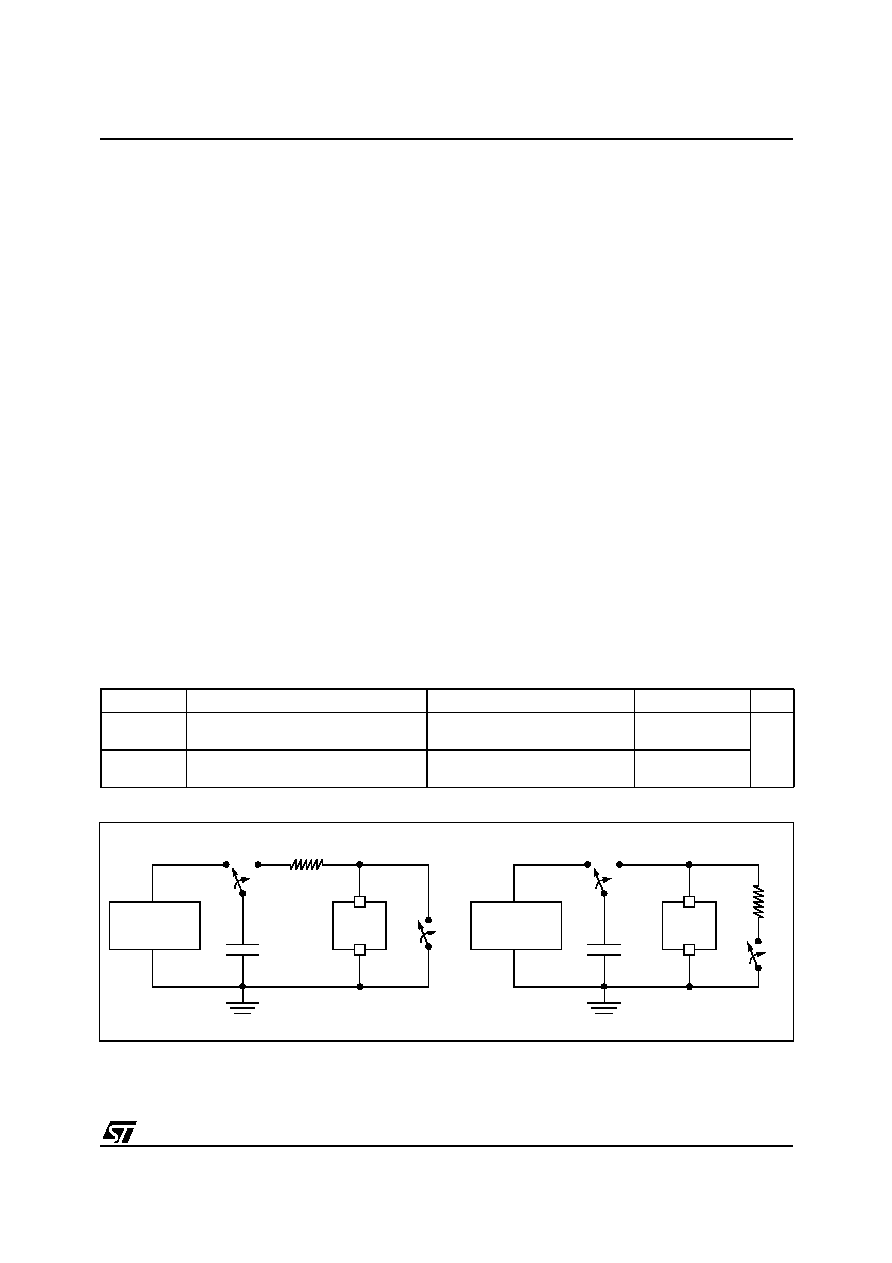
ST7LITE0, ST7SUPERLITE
91/122
EMC CHARACTERISTICS (Cont'd)
13.7.2 Absolute Electrical Sensitivity
Based on three different tests (ESD, LU and DLU)
using specific measurement methods, the product
is stressed in order to determine its performance in
terms of electrical sensitivity. For more details, re-
fer to the AN1181 ST7 application note.
13.7.2.1 Electro-Static Discharge (ESD)
Electro-Static Discharges (3 positive then 3 nega-
tive pulses separated by 1 second) are applied to
the pins of each sample according to each pin
combination. The sample size depends of the
number of supply pins of the device (3 parts*(n+1)
supply pin). Two models are usually simulated:
Human Body Model and Machine Model. This test
conforms to the JESD22-A114A/A115A standard.
See
Figure 61
and the following test sequences.
Human Body Model Test Sequence
≠ C
L
is loaded through S1 by the HV pulse gener-
ator.
≠ S1 switches position from generator to R.
≠ A discharge from C
L
through R (body resistance)
to the ST7 occurs.
≠ S2 must be closed 10 to 100ms after the pulse
delivery period to ensure the ST7 is not left in
charge state. S2 must be opened at least 10ms
prior to the delivery of the next pulse.
Machine Model Test Sequence
≠ C
L
is loaded through S1 by the HV pulse gener-
ator.
≠ S1 switches position from generator to ST7.
≠ A discharge from C
L
to the ST7 occurs.
≠ S2 must be closed 10 to 100ms after the pulse
delivery period to ensure the ST7 is not left in
charge state. S2 must be opened at least 10ms
prior to the delivery of the next pulse.
≠ R (machine resistance), in series with S2, en-
sures a slow discharge of the ST7.
Absolute Maximum Ratings
Figure 61. Typical Equivalent ESD Circuits
Notes:
1. Data based on characterization results, not tested in production.
Symbol
Ratings
Conditions
Maximum value
1)
Unit
V
ESD(HBM)
Electro-static discharge voltage
(Human Body Model)
T
A
=
+25∞C
4000
V
V
ESD(MM)
Electro-static discharge voltage
(Machine Model)
T
A
=
+25∞C
TBD
ST7
S2
R=1500
S1
HIGH VOLTAGE
C
L
=
100pF
PULSE
GENERATOR
ST7
S2
HIGH VOLTAGE
C
L
=
200pF
PULSE
GENERATOR
R
=
10
k
~
10M
S1
HUMAN BODY MODEL
MACHINE MODEL
1
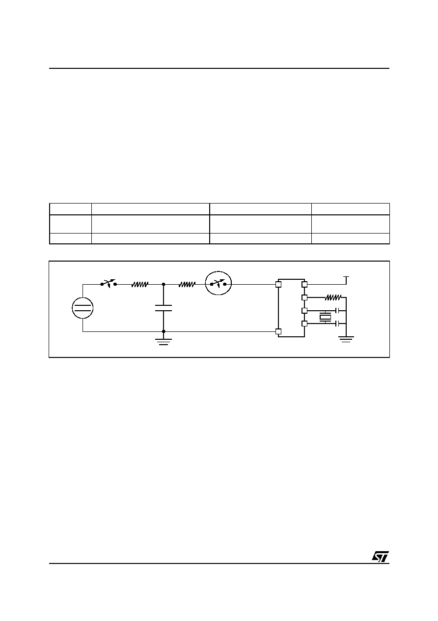
ST7LITE0, ST7SUPERLITE
92/122
EMC CHARACTERISTICS (Cont'd)
13.7.2.2 Static and Dynamic Latch-Up
s
LU: 3 complementary static tests are required
on 10 parts to assess the latch-up performance.
A supply overvoltage (applied to each power
supply pin), a current injection (applied to each
input, output and configurable I/O pin) and a
power supply switch sequence are performed
on each sample. This test conforms to the EIA/
JESD 78 IC latch-up standard. For more details,
refer to the AN1181 ST7 application note.
s
DLU: Electro-Static Discharges (one positive
then one negative test) are applied to each pin
of 3 samples when the micro is running to
assess the latch-up performance in dynamic
mode. Power supplies are set to the typical
values, the oscillator is connected as near as
possible to the pins of the micro and the
component is put in reset mode. This test
conforms to the IEC1000-4-2 and SAEJ1752/3
standards and is described in
Figure 62
. For
more details, refer to the AN1181 ST7
application note.
Electrical Sensitivities
Figure 62. Simplified Diagram of the ESD Generator for DLU
Notes:
1. Class description: A Class is an STMicroelectronics internal specification. All its limits are higher than the JEDEC spec-
ifications, that means when a device belongs to Class A it exceeds the JEDEC standard. B Class strictly covers all the
JEDEC criteria (international standard).
2. Schaffner NSG435 with a pointed test finger.
Symbol
Parameter
Conditions
Class
1)
LU
Static latch-up class
T
A
=
+25∞C
T
A
=
+85∞C
A
A
DLU
Dynamic latch-up class
V
DD
=
5.5V, f
OSC
=
4MHz, T
A
=
+25∞C
A
R
CH
=50M
R
D
=330
C
S
=
150pF
ESD
HV RELAY
DISCHARGE TIP
DISCHARGE
RETURN CONNECTION
GENERATOR
2)
ST7
V
DD
V
SS
1
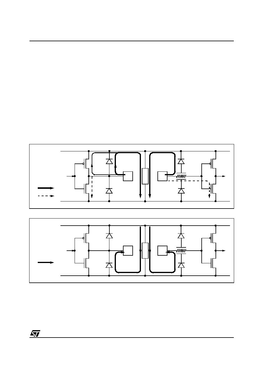
ST7LITE0, ST7SUPERLITE
93/122
EMC CHARACTERISTICS (Cont'd)
13.7.3 ESD Pin Protection Strategy
To protect an integrated circuit against Electro-
Static Discharge the stress must be controlled to
prevent degradation or destruction of the circuit el-
ements. The stress generally affects the circuit el-
ements which are connected to the pads but can
also affect the internal devices when the supply
pads receive the stress. The elements to be pro-
tected must not receive excessive current, voltage
or heating within their structure.
An ESD network combines the different input and
output ESD protections. This network works, by al-
lowing safe discharge paths for the pins subjected
to ESD stress. Two critical ESD stress cases are
presented in
Figure 63
and
Figure 64
for standard
pins.
Standard Pin Protection
To protect the output structure the following ele-
ments are added:
≠ A diode to V
DD
(3a) and a diode from V
SS
(3b)
≠ A protection device between V
DD
and V
SS
(4)
To protect the input structure the following ele-
ments are added:
≠ A resistor in series with the pad (1)
≠ A diode to V
DD
(2a) and a diode from V
SS
(2b)
≠ A protection device between V
DD
and V
SS
(4)
Figure 63. Positive Stress on a Standard Pad vs. V
SS
Figure 64. Negative Stress on a Standard Pad vs. V
DD
IN
V
DD
V
SS
(1)
(2a)
(2b)
(4)
OUT
V
DD
V
SS
(3a)
(3b)
Main path
Path to avoid
IN
V
DD
V
SS
(1)
(2a)
(2b)
(4)
OUT
V
DD
V
SS
(3a)
(3b)
Main path
1
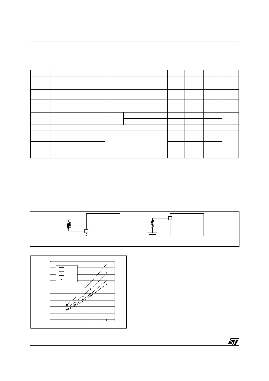
ST7LITE0, ST7SUPERLITE
94/122
13.8 I/O PORT PIN CHARACTERISTICS
13.8.1 General Characteristics
Subject to general operating conditions for V
DD
, f
OSC
, and T
A
unless otherwise specified.
Notes:
1. Data based on characterization results, not tested in production.
2. Configuration not recommended, all unused pins must be kept at a fixed voltage: using the output mode of the I/O for
example or an external pull-up or pull-down resistor (see
Figure 65
). Data based on design simulation and/or technology
characteristics, not tested in production.
3. The R
PU
pull-up equivalent resistor is based on a resistive transistor (corresponding I
PU
current characteristics de-
scribed in
Figure 66
).
4. To generate an external interrupt, a minimum pulse width has to be applied on an I/O port pin configured as an external
interrupt source.
Figure 65. Two typical Applications with unused I/O Pin
Figure 66. Typical I
PU
vs. V
DD
with V
IN
=V
SS
l
Symbol
Parameter
Conditions
Min
Typ
Max
Unit
V
IL
Input low level voltage
0.3xV
DD
V
V
IH
Input high level voltage
0.7xV
DD
V
hys
Schmitt trigger voltage
hysteresis
1)
400
mV
I
L
Input leakage current
V
SS
V
IN
V
DD
±1
µ
A
I
S
Static current consumption
2)
Floating input mode
200
R
PU
Weak pull-up equivalent
resistor
3)
V
IN
=
V
SS
V
DD
=5V
50
120
250
k
V
DD
=3V 160
C
IO
I/O pin capacitance
5
pF
t
f(IO)out
Output high to low level fall
time
1)
C
L
=50pF
Between 10% and 90%
25
ns
t
r(IO)out
Output low to high level rise
time
1)
25
t
w(IT)in
External interrupt pulse time
4)
1
t
CPU
10k
UNUSED I/O PORT
ST7XXX
10k
UNUSED I/O PORT
ST7XXX
V
DD
Note: only external pull-up allowed on ICCCLK pin
TO BE CHARACTERIZED
0
1 0
2 0
3 0
4 0
5 0
6 0
7 0
8 0
9 0
2
2.5
3
3.5
4
4.5
5
5.5
6
Vdd(V)
Ip
u
(
u
A
)
Ta=1 40∞C
Ta=9 5∞C
Ta=2 5∞C
Ta=-45 ∞C
1

ST7LITE0, ST7SUPERLITE
95/122
I/O PORT PIN CHARACTERISTICS (Cont'd)
13.8.2 Output Driving Current
Subject to general operating conditions for V
DD
, f
CPU
, and T
A
unless otherwise specified.
Notes:
1. The I
IO
current sunk must always respect the absolute maximum rating specified in
Section 13.2.2
and the sum of I
IO
(I/O ports and control pins) must not exceed I
VSS
.
2. The I
IO
current sourced must always respect the absolute maximum rating specified in
Section 13.2.2
and the sum of
I
IO
(I/O ports and control pins) must not exceed I
VDD
. True open drain I/O pins does not have V
OH
.
3. Not tested in production, based on characterization results.
Figure 67. Typical V
OL
at V
DD
=2.4V (standard)
Figure 68. Typical V
OL
at V
DD
=2.7V (standard)
Symbol
Parameter
Conditions
Min
Max
Unit
V
OL
1)
Output low level voltage for a standard I/O pin
when 8 pins are sunk at same time
(see
Figure 70
)
V
DD
=5V
I
IO
=+5mA
T
A
85∞C
T
A
85∞C
1.0
1.2
V
I
IO
=+2mA
T
A
85∞C
T
A
85∞C
0.4
0.5
Output low level voltage for a high sink I/O pin
when 4 pins are sunk at same time
(see
Figure 72
)
I
IO
=+20mA,T
A
85∞C
T
A
85∞C
1.3
1.5
I
IO
=+8mA
T
A
85∞C
T
A
85∞C
0.75
0.85
V
OH
2)
Output high level voltage for an I/O pin
when 4 pins are sourced at same time
(see
Figure 78
)
I
IO
=-5mA, T
A
85∞C
T
A
85∞C
V
DD
-1.5
V
DD
-1.6
I
IO
=-2mA
T
A
85∞C
T
A
85∞C
V
DD
-0.8
V
DD
-1.0
V
OL
1)3)
Output low level voltage for a standard I/O pin
when 8 pins are sunk at same time
(see
Figure 69
)
V
DD
=3.3V
I
IO
=+2mA
T
A
85∞C
T
A
85∞C
0.5
0.6
Output low level voltage for a high sink I/O pin
when 4 pins are sunk at same time
I
IO
=+8mA
T
A
85∞C
T
A
85∞C
0.5
0.6
V
OH
2)3)
Output high level voltage for an I/O pin
when 4 pins are sourced at same time
I
IO
=-2mA
T
A
85∞C
T
A
85∞C
V
DD
-0.8
V
DD
-1.0
V
OL
1)3)
Output low level voltage for a standard I/O pin
when 8 pins are sunk at same time
(see
Figure 68
)
V
DD
=2.
7
V
I
IO
=+2mA
T
A
85∞C
T
A
85∞C
0.6
0.7
Output low level voltage for a high sink I/O pin
when 4 pins are sunk at same time
I
IO
=+8mA
T
A
85∞C
T
A
85∞C
0.6
0.7
V
OH
2)3)
Output high level voltage for an I/O pin
when 4 pins are sourced at same time
(see
Figure 75
)
I
IO
=-2mA
T
A
85∞C
T
A
85∞C
V
DD
-0.9
V
DD
-1.0
TO BE CHARACTERIZED
0.00
0.10
0.20
0.30
0.40
0.50
0.60
0.70
0.01
1
2
lio (mA)
V
O
L at
V
D
D
=
2.
4V
-45
0∞C
25∞C
90∞C
130∞C
0.00
0.10
0.20
0.30
0.40
0.50
0.60
0.01
1
2
lio (mA)
V
O
L at
V
D
D
=
2.
7V
-45∞C
0∞C
25∞C
90∞C
130∞C
1
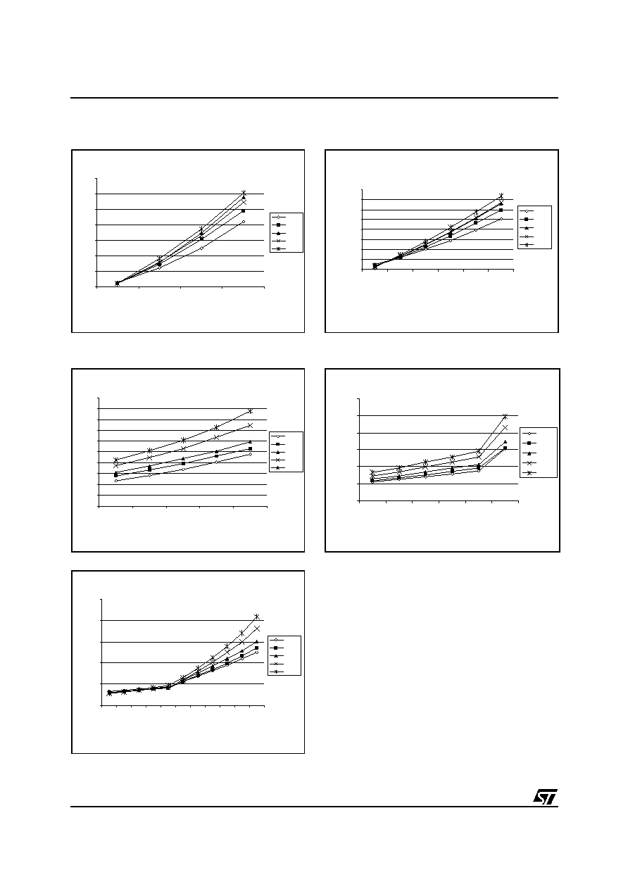
ST7LITE0, ST7SUPERLITE
96/122
I/O PORT PIN CHARACTERISTICS (Cont'd)
Figure 69. Typical V
OL
at V
DD
=3.3V (standard)
Figure 70. Typical V
OL
at V
DD
=5V (standard)
Figure 71. Typical V
OL
at V
DD
=2.4V (high-sink)
Figure 72. Typical V
OL
at V
DD
=5V (high-sink)
Figure 73. Typical V
OL
at V
DD
=3V (high-sink)
0.00
0.10
0.20
0.30
0.40
0.50
0.60
0.70
0.01
1
2
3
lio (mA)
V
O
L at V
D
D
=
3.3V
-45∞C
0∞C
25∞C
90∞C
130∞C
0.00
0.10
0.20
0.30
0.40
0.50
0.60
0.70
0.80
0.01
1
2
3
4
5
lio (mA)
V
O
L at
V
D
D
=
5V
-45∞C
0∞C
25∞C
90∞C
130∞C
0.00
0.10
0.20
0.30
0.40
0.50
0.60
0.70
0.80
0.90
1.00
6
7
8
9
10
lio (mA)
V
O
L at V
D
D
=
2.4V
(
H
S
)
-45
0∞C
25∞C
90∞C
130∞C
0.00
0.50
1.00
1.50
2.00
2.50
6
7
8
9
10
15
20
25
30
35
40
lio (mA)
V
o
l
(V
) a
t
V
D
D
=
5
V
(H
S
)
-45
0∞C
25∞C
90∞C
130∞C
0.00
0.20
0.40
0.60
0.80
1.00
1.20
6
7
8
9
10
15
lio (mA)
V
o
l
(V
) a
t
V
DD=3
V
(HS
)
-45
0∞C
25∞C
90∞C
130∞C
1
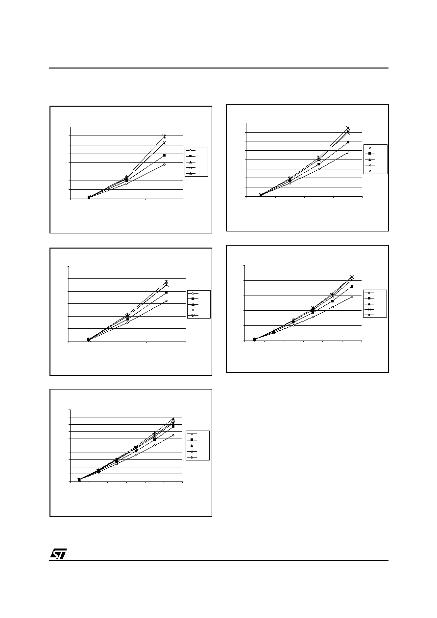
ST7LITE0, ST7SUPERLITE
97/122
I/O PORT PIN CHARACTERISTICS (Cont'd)
Figure 74. Typical V
DD
-V
OH
at V
DD
=2.4V
Figure 75. Typical V
DD
-V
OH
at V
DD
=2.7V
Figure 76. Typical V
DD
-V
OH
at V
DD
=3V
Figure 77. Typical V
DD
-V
OH
at V
DD
=4V
Figure 78. Typical V
DD
-V
OH
at V
DD
=5V
0.00
0.20
0.40
0.60
0.80
1.00
1.20
1.40
1.60
-0.01
-1
-2
lio (mA)
V
DD-
V
O
H a
t
V
DD=
2
.
4
V
-45∞C
0∞C
25∞C
90∞C
130∞C
0.00
0.20
0.40
0.60
0.80
1.00
1.20
-0.01
-1
-2
lio(mA)
V
DD-
V
O
H a
t
V
DD=2
.
7
V
-45∞C
0∞C
25∞C
90∞C
130∞C
0.00
0.20
0.40
0.60
0.80
1.00
1.20
1.40
1.60
-0.01
-1
-2
-3
lio (mA)
V
DD-
V
O
H a
t
V
DD=
3
V
-45∞C
0∞C
25∞C
90∞C
130∞C
0.00
0.50
1.00
1.50
2.00
2.50
-0.01
-1
-2
-3
-4
-5
lio (mA)
V
DD-
V
O
H a
t
V
DD=4
V
-45∞C
0∞C
25∞C
90∞C
130∞C
TO BE CHARACTERIZED
0.00
0.20
0.40
0.60
0.80
1.00
1.20
1.40
1.60
1.80
2.00
-0.01
-1
-2
-3
-4
-5
lio (mA)
V
DD-
V
O
H a
t
V
DD=
5
V
-45∞C
0∞C
25∞C
90∞C
130∞C
1
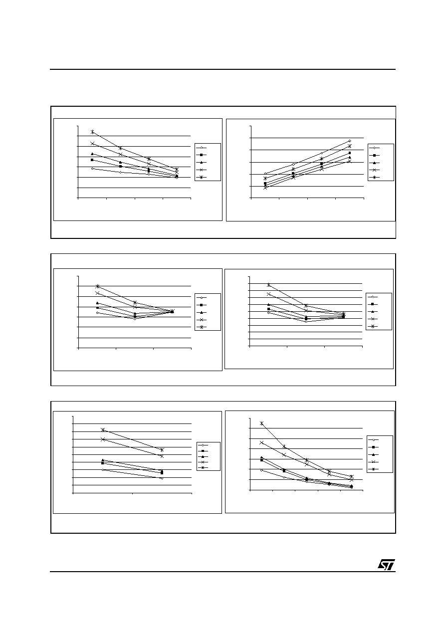
ST7LITE0, ST7SUPERLITE
98/122
I/O PORT PIN CHARACTERISTICS (Cont'd)
Figure 79. Typical V
OL
vs. V
DD
(standard I/Os)
Figure 80. Typical V
OL
vs. V
DD
(high-sink I/Os)
Figure 81. Typical V
DD
-V
OH
vs. V
DD
0.00
0.10
0.20
0.30
0.40
0.50
0.60
0.70
2.4
2.7
3.3
5
VDD (V)
Vo
l (
V
)
at
lio
=
2
m
A
-45
0∞C
25∞C
90∞C
130∞C
0.00
0.01
0.02
0.03
0.04
0.05
0.06
2.4
2.7
3.3
5
VDD (V)
Vo
l (
V
)
at
lio
=
0
.01m
A
-45
0∞C
25∞C
90∞C
130∞C
0.00
0.10
0.20
0.30
0.40
0.50
0.60
0.70
2.4
3
5
VDD (V)
VO
L
v
s
VD
D
(
H
S)
a
t
lio
=8
m
A
-45
0∞C
25∞C
90∞C
130∞C
0.00
0.10
0.20
0.30
0.40
0.50
0.60
0.70
0.80
0.90
1.00
2.4
3
5
VDD (V)
V
O
L
vs V
D
D
(
H
S
)
at
lio
=
20m
A
-45
0∞C
25∞C
90∞C
130∞C
0.40
0.50
0.60
0.70
0.80
0.90
1.00
1.10
2.4
2.7
3
4
5
VDD (V)
V
DD-V
O
H (V
) a
t
l
i
o
=
-
2
m
A
-45∞C
0∞C
25∞C
90∞C
130∞C
0.80
0.90
1.00
1.10
1.20
1.30
1.40
1.50
1.60
1.70
1.80
4
5
VDD
V
DD-
V
O
H a
t
l
i
o
=-
5
m
A
-45∞C
0∞C
25∞C
90∞C
130∞C
1

ST7LITE0, ST7SUPERLITE
99/122
13.9 CONTROL PIN CHARACTERISTICS
13.9.1 Asynchronous RESET Pin
T
A
= -40∞C to 125∞C, unless otherwise specified
Figure 82. Typical Application with RESET pin
6)7)8)
Notes:
1. Data based on characterization results, not tested in production.
2. The I
IO
current sunk must always respect the absolute maximum rating specified in
Section 13.2.2
and the sum of I
IO
(I/O ports and control pins) must not exceed I
VSS
.
3. The R
ON
pull-up equivalent resistor is based on a resistive transistor. Specfied for voltages on RESET pin between
V
ILmax
and V
DD
4. To guarantee the reset of the device, a minimum pulse has to be applied to the RESET pin. All short pulses applied on
RESET pin with a duration below t
h(RSTL)in
can be ignored.
5. The reset network protects the device against parasitic resets.
6. The output of the external reset circuit must have an open-drain output to drive the ST7 reset pad. Otherwise the device
can be damaged when the ST7 generates an internal reset (LVD or watchdog).
7. Whatever the reset source is (internal or external), the user must ensure that the level on the RESET pin can go below
the V
IL
max. level specified in
section 13.9.1 on page 99
. Otherwise the reset will not be taken into account internally.
8. Because the reset circuit is designed to allow the internal RESET to be output in the RESET pin, the user must ensure
that the current sunk on the RESET pin (by an external pull-p for example) is less than the absolute maximum value spec-
ified for I
INJ(RESET)
in
section 13.2.2 on page 79
.
Symbol
Parameter
Conditions
Min
Typ
Max
Unit
V
IL
Input low level voltage
0.3xV
DD
V
V
IH
Input high level voltage
0.7xV
DD
V
hys
Schmitt trigger voltage hysteresis
1)
1
V
V
OL
Output low level voltage
2)
V
DD
=5V
I
IO
=+5mA T
A
85∞C
T
A
85∞C
0.5
1.0
1.2
V
I
IO
=+2mA T
A
85∞C
T
A
85∞C
0.2
0.4
0.5
R
ON
Pull-up equivalent resistor
3) 1)
V
DD
=5V 20
40
80
k
V
DD
=3V
TBD
t
w(RSTL)out
Generated reset pulse duration
Internal reset sources
30
µ
s
t
h(RSTL)in
External reset pulse hold time
4)
20
µ
s
t
g(RSTL)in
Filtered glitch duration
5)
200
ns
R
ON
0.01
µ
F
V
DD
0.01
µ
F
EXTERNAL
RESET
CIRCUIT
5)
USER
V
DD
4.7k
Required if LVD is disabled
Recommended
if LVD is disabled
ST72XXX
PULSE
GENERATOR
Filter
WATCHDOG
LVD RESET
INTERNAL
RESET
V
DD
1
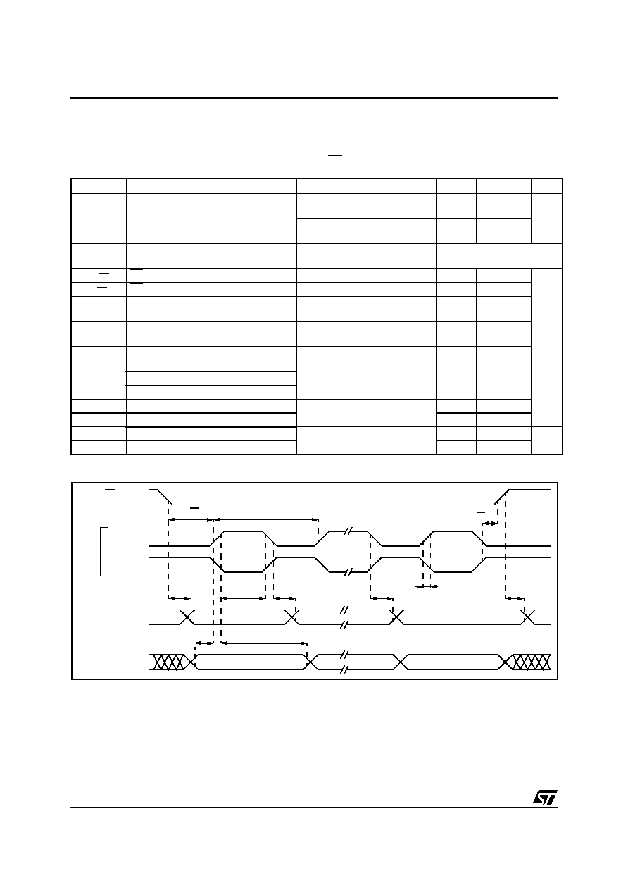
ST7LITE0, ST7SUPERLITE
100/122
13.10 COMMUNICATION INTERFACE CHARACTERISTICS
13.10.1 SPI - Serial Peripheral Interface
Subject to general operating conditions for V
DD
,
f
OSC
, and T
A
unless otherwise specified.
Refer to I/O port characteristics for more details on
the input/output alternate function characteristics
(SS, SCK, MOSI, MISO).
Figure 83. SPI Slave Timing Diagram with CPHA=0
3)
Notes:
1. Data based on design simulation and/or characterisation results, not tested in production.
2. When no communication is on-going the data output line of the SPI (MOSI in master mode, MISO in slave mode) has
its alternate function capability released. In this case, the pin status depends on the I/O port configuration.
3. Measurement points are done at CMOS levels: 0.3xV
DD
and 0.7xV
DD
.
Symbol
Parameter
Conditions
Min
Max
Unit
f
SCK
1/t
c(SCK)
SPI clock frequency
Master
f
CPU
=8MHz
f
CPU
/128
0.0625
f
CPU
/42
MHz
Slave
f
CPU
=8MHz
0
f
CPU
/24
t
r(SCK)
t
f(SCK)
SPI clock rise and fall time
see I/O port pin description
t
su(SS)
SS setup time
Slave
120
ns
t
h(SS)
SS hold time
Slave
120
t
w(SCKH)
t
w(SCKL)
SCK high and low time
Master
Slave
100
90
t
su(MI)
t
su(SI)
Data input setup time
Master
Slave
100
100
t
h(MI)
t
h(SI)
Data input hold time
Master
Slave
100
100
t
a(SO)
Data output access time
Slave
0
120
t
dis(SO)
Data output disable time
Slave
240
t
v(SO)
Data output valid time
Slave (after enable edge)
120
t
h(SO)
Data output hold time
0
t
v(MO)
Data output valid time
Master (before capture edge)
0.25
t
CPU
t
h(MO)
Data output hold time
0.25
SS
INPUT
SC
K
INP
U
T
CPHA=0
MOSI
INPUT
MISO
OUTPUT
CPHA=0
t
c(SCK)
t
w(SCKH)
t
w(SCKL)
t
r(SCK)
t
f(SCK)
t
v(SO)
t
a(SO)
t
su(SI)
t
h(SI)
MSB OUT
MSB IN
BIT6 OUT
LSB IN
LSB OUT
see note 2
CPOL=0
CPOL=1
t
su(SS)
t
h(SS)
t
dis(SO)
t
h(SO)
see
note 2
BIT1 IN
1
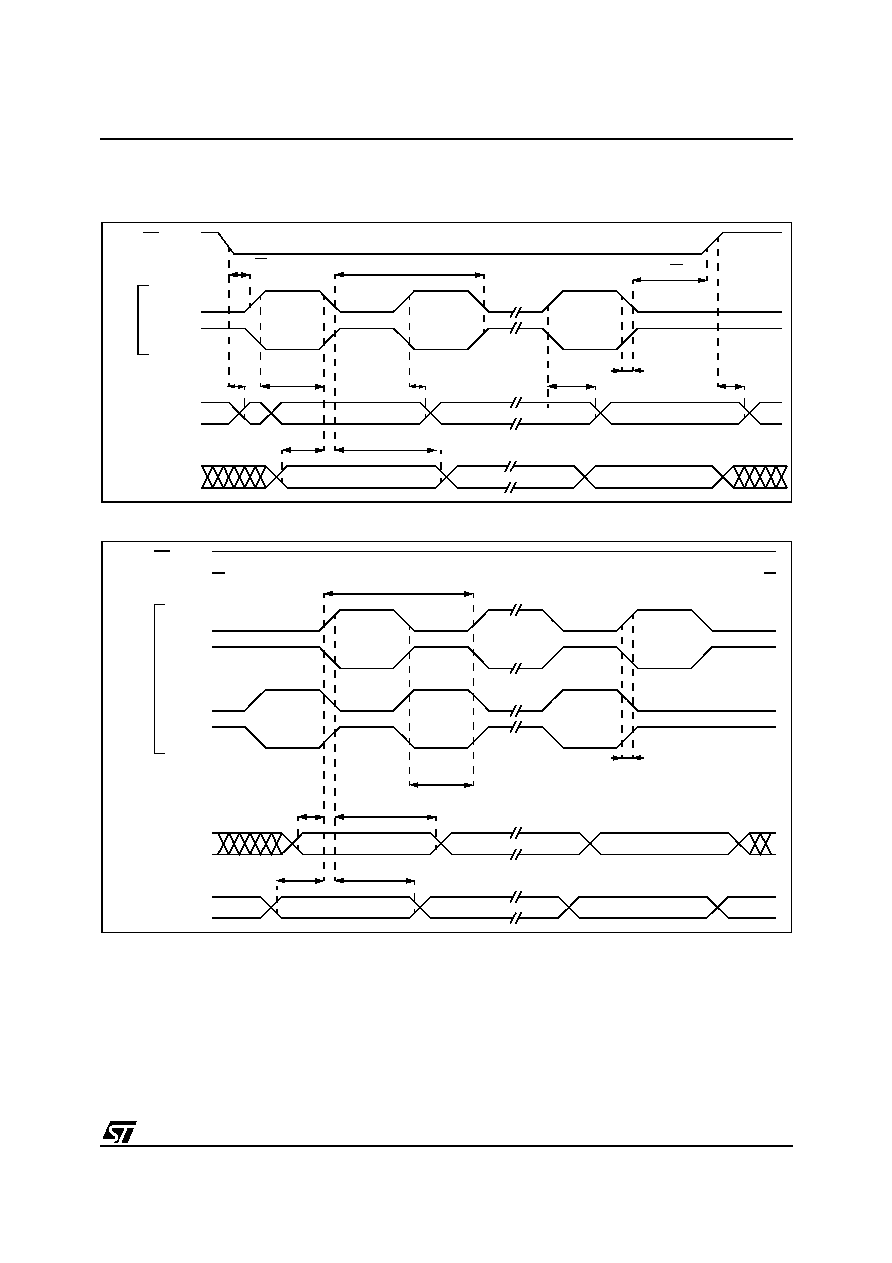
ST7LITE0, ST7SUPERLITE
101/122
COMMUNICATION INTERFACE CHARACTERISTICS (Cont'd)
Figure 84. SPI Slave Timing Diagram with CPHA=1
1)
Figure 85. SPI Master Timing Diagram
1)
Notes:
1. Measurement points are done at CMOS levels: 0.3xV
DD
and 0.7xV
DD
.
2. When no communication is on-going the data output line of the SPI (MOSI in master mode, MISO in slave mode) has
its alternate function capability released. In this case, the pin status depends of the I/O port configuration.
SS
INPUT
SC
K
INP
U
T
CPHA=0
MOSI
INPUT
MISO
OUTPUT
CPHA=0
t
w(SCKH)
t
w(SCKL)
t
r(SCK)
t
f(SCK)
t
a(SO)
t
su(SI)
t
h(SI)
MSB OUT
BIT6 OUT
LSB OUT
see
CPOL=0
CPOL=1
t
su(SS)
t
h(SS)
t
dis(SO)
t
h(SO)
see
note 2
note 2
t
c(SCK)
HZ
t
v(SO)
MSB IN
LSB IN
BIT1 IN
SS
INPUT
SC
K
INP
U
T
CPHA=0
MOSI
OUTPUT
MISO
INPUT
CPHA=0
CPHA=1
CPHA=1
t
c(SCK)
t
w(SCKH)
t
w(SCKL)
t
h(MI)
t
su(MI)
t
v(MO)
t
h(MO)
MSB IN
MSB OUT
BIT6 IN
BIT6 OUT
LSB OUT
LSB IN
see note 2
see note 2
CPOL=0
CPOL=1
CPOL=0
CPOL=1
t
r(SCK)
t
f(SCK)
1
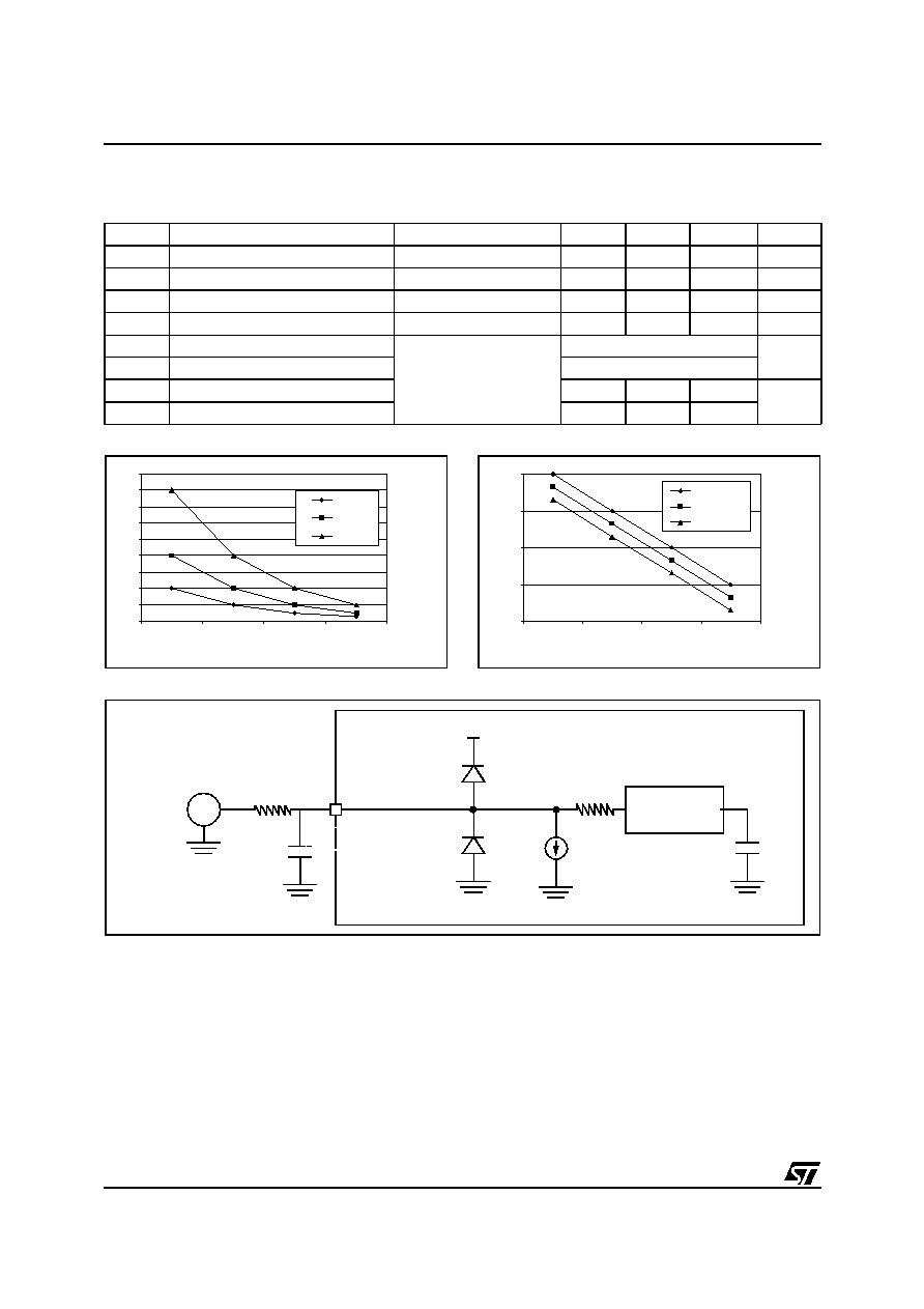
ST7LITE0, ST7SUPERLITE
102/122
13.11 8-BIT ADC CHARACTERISTICS
T
A
= -40∞C to 125∞C, unless otherwise specified
Figure 86. R
AIN
max. vs f
ADC
with C
AIN
=0pF
3)
Figure 87. Recommended C
AIN
/R
AIN
values
4)
Figure 88. Typical Application with ADC
Notes:
1. Any added external serial resistor will downgrade the ADC accuracy (especially for resistance greater than 10k
). Data
based on characterization results, not tested in production.
2. The stabilization time of the AD converter is masked by the first tLOAD. The first conversion after the enable is then
always valid.
3.C
PARASITIC
represents the capacitance of the PCB (dependent on soldering and PCB layout quality) plus the pad ca-
pacitance (3pF). A high C
PARASITIC
value will downgrade conversion accuracy. To remedy this, f
ADC
should be reduced.
4. This graph shows that depending on the input signal variation (f
AIN
), C
AIN
can be increased for stabilization and to allow
the use of a larger serial resistor (R
AIN)
. It is valid for all f
ADC
frequencies
4MHz.
Symbol
Parameter
Conditions
Min
Typ
Max
Unit
f
ADC
ADC clock frequency
4
MHz
V
AIN
Conversion voltage range
V
SS
V
DD
V
R
AIN
External input resistor
10
1)
k
C
ADC
Internal sample and hold capacitor
V
DD
=5V
3
pF
t
STAB
Stabilization time after ADC enable
f
CPU
=8MHz, f
ADC
=4MHz
0
2)
µ
s
t
CONV
Conversion time (t
SAMPLE
+t
HOLD
)
3
t
SAMPLE
Sample capacitor loading time
4
1/f
ADC
t
HOLD
Hold conversion time
8
0
5
10
15
20
25
30
35
40
45
0
10
30
70
C
PARASITIC
(pF)
Max
.
R
AI
N
(
K
ohm)
4 MHz
2 MHz
1 MHz
0.1
1
10
100
1000
0.01
0.1
1
10
f
AIN
(KHz)
Max
.
R
AI
N
(
K
ohm)
Cain 10 nF
Cain 22 nF
Cain 47 nF
AINx
ST72XXX
V
DD
I
L
±1
µ
A
V
T
0.6V
V
T
0.6V
C
ADC
3pF
V
AIN
R
AIN
8-Bit A/D
Conversion
2k
(
max
)
C
AIN
1
ST7LITE0, ST7SUPERLITE
103/122
ADC CHARACTERISTICS (Cont'd)
13.11.0.1 General PCB Design Guidelines
To obtain best results, some general design and
layout rules should be followed when designing
the application PCB to shield the noise-sensitive,
analog physical interface from noise-generating
CMOS logic signals.
≠ Properly place components and route the signal
traces on the PCB to shield the analog inputs.
Analog signals paths should run over the analog
ground plane and be as short as possible. Isolate
analog signals from digital signals that may
switch while the analog inputs are being sampled
by the A/D converter. Do not toggle digital out-
puts on the same I/O port as the A/D input being
converted.
ADC Accuracy
T
A
= -40∞C to 85∞C, unless otherwise specified
Notes:
1) Data based on characterization results over the whole temperature range, monitored in production.
2) Injecting negative current on any of the analog input pins significantly reduces the accuracy of any conversion being
performed on any analog input.
Analog pins can be protected against negative injection by adding a Schottky diode (pin to ground). Injecting negative
current on digital input pins degrades ADC accuracy especially if performed on a pin close to the analog input pins.
Any positive injection current within the limits specified for I
INJ(PIN)
and
I
INJ(PIN)
in
Section 13.8
does not affect the ADC
accuracy.
Symbol
Parameter
Conditions
Typ
Max
Unit
E
T
Total unadjusted error
2)
f
CPU
=4MHz, f
ADC
=2MHz ,V
DD
=5.0V
±1
LSB
E
O
Offset error
2)
-0.5 / +1
E
G
Gain Error
2)
±1
E
D
Differential linearity error
2)
±1
1)
E
L
Integral linearity error
2)
±1
1)
E
T
Total unadjusted error
2)
f
CPU
=8MHz, f
ADC
=4MHz ,V
DD
=5.0V
±2
LSB
E
O
Offset error
2)
-0.5 / 3.5
E
G
Gain Error
2)
-2 / 0
E
D
Differential linearity error
2)
±1
1)
E
L
Integral linearity error
2)
±1
1)
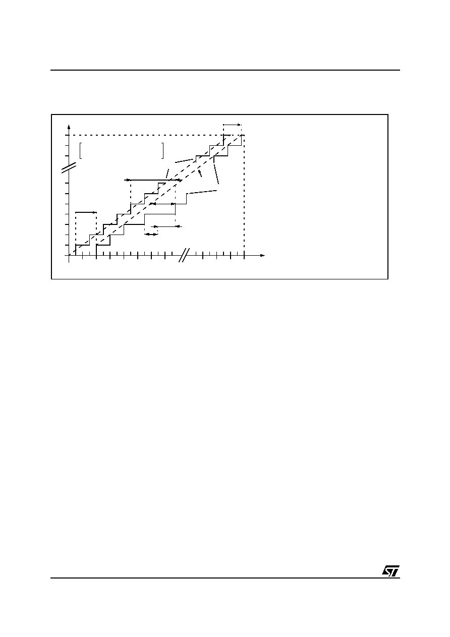
ST7LITE0, ST7SUPERLITE
104/122
ADC CHARACTERISTICS (Cont'd)
Figure 89. ADC Accuracy Characteristics with Amplifier disabled
E
O
E
G
1 LSB
IDEAL
1LSB
IDEAL
V
DDA
V
S SA
≠
256
-----------------------------------------
=
V
in
(LSB
IDEAL
)
(1) Example of an actual transfer curve
(2) The ideal transfer curve
(3) End point correlation line
E
T
=Total Unadjusted Error: maximum deviation
between the actual and the ideal transfer curves.
E
O
=Offset Error: deviation between the first actual
transition and the first ideal one.
E
G
=Gain Error: deviation between the last ideal
transition and the last actual one.
E
D
=Differential Linearity Error: maximum deviation
between actual steps and the ideal one.
E
L
=Integral Linearity Error: maximum deviation
between any actual transition and the end point
correlation line.
Digital Result ADCDR
255
254
5
4
3
2
1
0
7
6
1
2
3
4
5
6
7
253 254 255 256
(1)
(2)
E
T
E
D
E
L
(3)
V
DDA
V
SSA
253
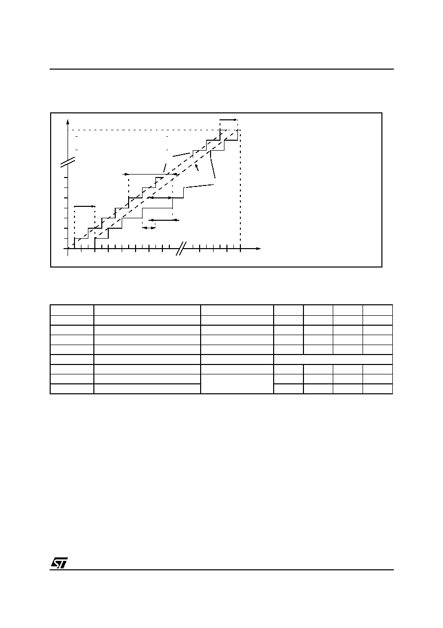
ST7LITE0, ST7SUPERLITE
105/122
ADC CHARACTERISTICS (Cont'd)
Figure 90. ADC Accuracy Characteristics with Amplifier enabled
Note: When the AMPSEL bit in the ADCDRL register is set, it is mandatory that f
ADC
be less than or equal
to 2 MHz. (if f
CPU
=8MHz. then SPEED=0, SLOW=1).
Notes:
1) Data based on characterization results over the whole temperature range, not tested in production.
2) For precise conversion results it is recommended to calibrate the amplifier at the following two points:
≠ offset at V
INmin
= 0V
≠ gain at full scale (for example V
IN
=250mV)
3) Monotonicity guaranteed if V
IN
increases or decreases in steps of min. 5mV.
E
O
E
G
1 LSB
IDEAL
V
in
(LSB
IDEAL
)
(1) Example of an actual transfer curve
(2) The ideal transfer curve
(3) End point correlation line
E
T
=Total Unadjusted Error: maximum deviation
between the actual and the ideal transfer curves.
E
O
=Offset Error: deviation between the first actual
transition and the first ideal one.
E
G
=Gain Error: deviation between the last ideal
transition and the last actual one.
E
D
=Differential Linearity Error: maximum deviation
between actual steps and the ideal one.
E
L
=Integral Linearity Error: maximum deviation
between any actual transition and the end point
correlation line.
n=Amplifier Offset
Digital Result ADCDR
n+5
n+4
n+3
n+2
n+1
0
n+7
n+6
1
2
3
4
5
6
7
100 101 102 103
(1)
(2)
E
T
E
D
E
L
(3)
250 mV
V
SS
1LSB
IDE AL
V
DDA
V
SSA
≠
103
8
◊
--------------------------------------
=
Symbol
Parameter
Conditions
Min
Typ
Max
Unit
V
DD(AMP)
Amplifier operating voltage
4.5
5.5
V
V
IN
Amplifier input voltage
V
DD
=5V
0
250
mV
V
OFFSET
Amplifier offset voltage
200
mV
V
STEP
Step size for monotonicity
3)
5
mV
Linearity
Output Voltage Response
Linear
Gain factor
Amplified Analog input Gain
2)
7
1)
8
9
1)
Vmax
Output Linearity Max Voltage
V
INmax
= 250mV,
V
DD
=5V
2.05
2.2
2.4
V
Vmin
Output Linearity Min Voltage
0
1)
0.22
0.25
V
ST7LITE0, ST7SUPERLITE
106/122
14 PACKAGE CHARACTERISTICS
14.1 PACKAGE MECHANICAL DATA
Figure 91. 16-Pin Plastic Dual In-Line Package, 300-mil Width
Figure 92. 16-Pin Plastic Small Outline Package, 150-mil Width
Dim.
mm
inches
Min
Typ
Max
Min
Typ
Max
A
5.33
0.210
A1
0.38
0.015
A2
2.92
3.30
4.95 0.115 0.130 0.195
b
0.36
0.46
0.56 0.014 0.018 0.022
b2
1.14
1.52
1.78 0.045 0.060 0.070
b3
0.76
0.99
1.14 0.030 0.039 0.045
c
0.20
0.25
0.36 0.008 0.010 0.014
D
18.67 19.18 19.69 0.735 0.755 0.775
D1
0.13
0.005
e
2.54
0.100
E
7.62
7.87
8.26 0.300 0.310 0.325
E1
6.10
6.35
7.11 0.240 0.250 0.280
L
2.92
3.30
3.81 0.115 0.130 0.150
eB
10.92
0.430
Number of Pins
N
16
c
E
E1
eB
L
A
A2
A1
e
b
b2
b3
D1
D
Dim.
mm
inches
Min
Typ
Max
Min
Typ
Max
A
1.35
1.75 0.053
0.069
A1
0.10
0.25 0.004
0.010
B
0.33
0.51 0.013
0.020
C
0.19
0.25 0.007
0.010
D
9.80
10.00 0.386
0.394
E
3.80
4.00 0.150
0.157
e
1.27
0.050
H
5.80
6.20 0.228
0.244
0∞
8∞
0∞
8∞
L
0.40
1.27 0.016
0.050
Number of Pins
N
16
0016020
E
H
A1
C
a
45◊
A1
A
B
D
e
16
9
1
8
L

ST7LITE0, ST7SUPERLITE
107/122
14.2 THERMAL CHARACTERISTICS
Notes:
1. The power dissipation is obtained from the formula P
D
=P
INT
+P
PORT
where P
INT
is the chip internal power (I
DD
xV
DD
)
and P
PORT
is the port power dissipation determined by the user.
2. The average chip-junction temperature can be obtained from the formula T
J
= T
A
+ P
D
x RthJA.
Symbol
Ratings
Value
Unit
R
thJA
Package thermal resistance (junction to ambient)
TBD
∞C/W
P
D
Power dissipation
1)
500
mW
T
Jmax
Maximum junction temperature
2)
150
∞C
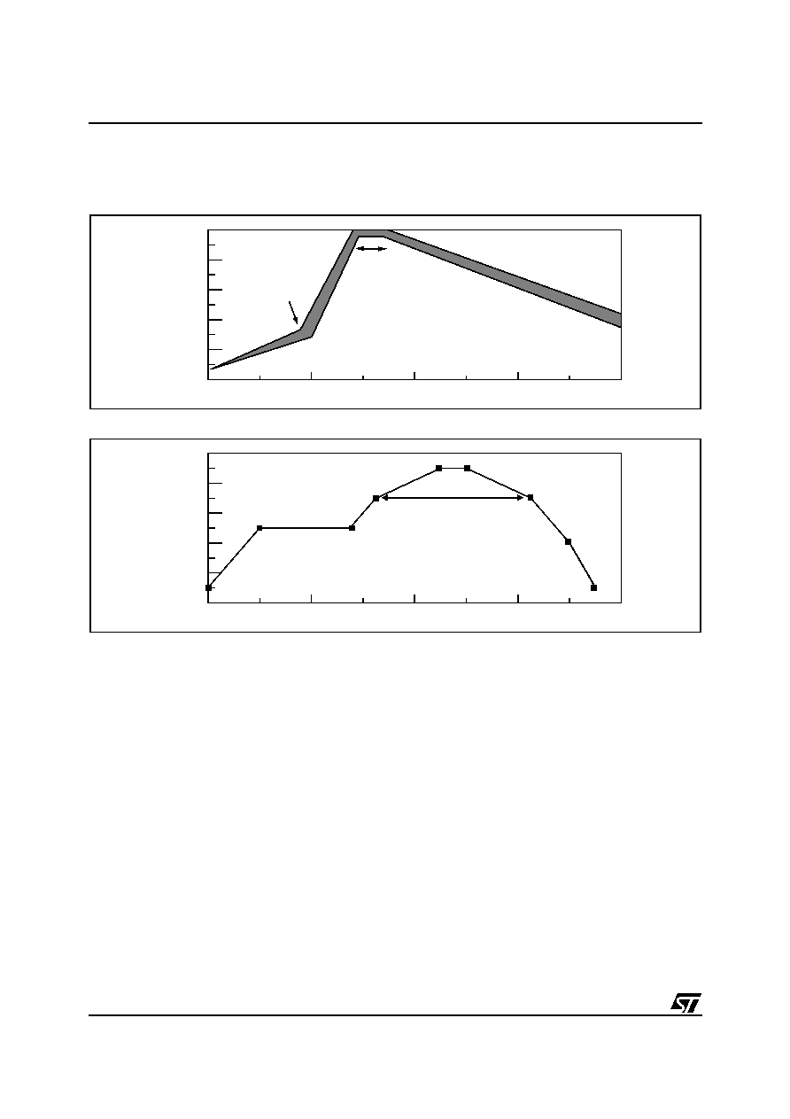
ST7LITE0, ST7SUPERLITE
108/122
14.3 SOLDERING AND GLUEABILITY INFORMATION
Recommended soldering information given only as design guidelines.
Figure 93. Recommended Wave Soldering Profile (with 37% Sn and 63% Pb)
Figure 94. Recommended Reflow Soldering Oven Profile (MID JEDEC)
Recommended glue for SMD plastic packages:
s
Heraeus: PD945, PD955
s
Loctite: 3615, 3298
250
200
150
100
50
0
40
80
120
160
Time [sec]
Temp. [∞C]
20
60
100
140
5 sec
COOLING PHASE
(ROOM TEMPERATURE)
PREHEATING
80∞C
PHASE
SOLDERING
PHASE
SOLDERING
250
200
150
100
50
0
100
200
300
400
Time [sec]
Temp. [∞C]
ramp up
2∞C/sec for 50sec
90 sec at 125∞C
150 sec above 183∞C
ramp down natural
2∞C/sec max
Tmax=220+/-5∞C
for 25 sec

ST7LITE0, ST7SUPERLITE
109/122
15 DEVICE CONFIGURATION AND ORDERING INFORMATION
Each device is available for production in user pro-
grammable versions (FLASH) as well as in factory
coded versions (FASTROM).
ST7PLITE0x and ST7PLITES2/S5 devices are
Factory Advanced Service Technique ROM (FAS-
TROM) versions: they are factory-programmed
XFlash devices.
ST7FLITE0x and ST7FLITES2/S5 XFlash devices
are shipped to customers with a default program
memory content (FFh). The OSC option bit is pro-
grammed to 0 by default.
The FASTROM factory coded parts contain the
code supplied by the customer. This implies that
FLASH devices have to be configured by the cus-
tomer using the Option Bytes while the FASTROM
devices are factory-configured.
15.1 OPTION BYTES
The two option bytes allow the hardware configu-
ration of the microcontroller to be selected.
The option bytes can be accessed only in pro-
gramming mode (for example using a standard
ST7 programming tool).
OPTION BYTE 0
Bit 7:4 = Reserved, must always be 1.
Bit 3:2 = SEC[1:0]
Sector 0 size definition
These option bits indicate the size of sector 0 ac-
cording to the following table.
Note 1: Configuration available for ST7LITE0 de-
vices only.
Bit 1 = FMP_R
Read-out protection
This option indicates if the FLASH program mem-
ory and Data EEPROM is protected against pira-
cy. The read-out protection blocks access to the
program and data areas in any mode except user
mode and IAP mode. Erasing the option bytes
when the FMP_R option is selected will cause the
whole memory to be erased first, , and the device
can be reprogrammed. Refer to
Section 4.5
and
the ST7 Flash Programming Reference Manual for
more details.
0: Read-out protection off
1: Read-out protection on
Bit 0 = FMP_W
FLASH write protection
This option indicates if the FLASH program mem-
ory is write protected.
Warning: When this option is selected, the pro-
gram memory (and the option bit itself) can never
be erased or programmed again.
0: Write protection off
1: Write protection on
Sector 0 Size
SEC1
SEC0
0.5k
0
0
1k
0
1
1.5k
1)
1
x
ST7LITE0, ST7SUPERLITE
110/122
OPTION BYTES (Cont'd)
OPTION BYTE 1
Bit 7 = PLLx4x8
PLL Factor selection.
0: PLLx4
1: PLLx8
Bit 6 = PLLOFF
PLL disable.
0: PLL enabled
1: PLL disabled (by-passed)
Bit 5 = Reserved, must always be 1.
Bit 4 = OSC
RC
Oscillator selection
0: RC oscillator on
1: RC oscillator off
Table 20. List of valid option combinations
Note 1: see Clock Management Block diagram in
Figure 13
Bit 3:2 = LVD[1:0]
Low voltage detection selection
These option bits enable the LVD block with a se-
lected threshold as shown in
Table 21
.
Table 21. LVD Threshold Configuration
Bit 1 = WDG SW
Hardware or software watchdog
This option bit selects the watchdog type.
0: Hardware (watchdog always enabled)
1: Software (watchdog to be enabled by software)
Bit 0 = WDG HALT
Watchdog Reset on Halt
This option bit determines if a RESET is generated
when entering HALT mode while the Watchdog is
active.
0: No Reset generation when entering Halt mode
1: Reset generation when entering Halt mode
Operating conditions
Option Bits
V
DD
range
Clock Source
PLL
Typ f
CPU
OSC
PLLOFF
PLLx4x8
2.4V - 3.3V
Internal RC 1%
off
0.7MHz @3V
0
1
x
x4
2.8MHz @3V
0
0
0
x8
-
-
-
-
External clock
off
0-4MHz
1
1
x
x4
4MHz
1
0
0
x8
-
-
-
-
3.3V - 5.5V
Internal RC 1%
off
1MHz @5V
0
1
x
x4
-
-
-
-
x8
8MHz @5V
0
0
1
External clock
off
0-8MHz
1
1
x
x4
-
-
-
-
x8
8 MHz
1
0
1
Configuration
LVD1 LVD0
LVD Off
1
1
Highest Voltage Threshold (
4.1V)
1
0
Medium Voltage Threshold (
3.5V)
0
1
Lowest Voltage Threshold (
2.8V)
0
0
OPTION BYTE 0
7
0
OPTION BYTE 1
7
0
Reserved SEC1 SEC0
FMP
R
FMP
W
PLL
x4x8
PLL
OFF
OSC LVD1 LVD0
WDG
SW
WDG
HALT
Default
Value
1
1
1
1
1
1
0
0
1
1
1
0
1
1
1
1

ST7LITE0, ST7SUPERLITE
111/122
15.2 DEVICE ORDERING INFORMATION AND TRANSFER OF CUSTOMER CODE
Customer code is made up of the FASTROM con-
tents and the list of the selected options (if any).
The FASTROM contents are to be sent on dis-
kette, or by electronic means, with the S19 hexa-
decimal file generated by the development tool. All
unused bytes must be set to FFh. The selected op-
tions are communicated to STMicroelectronics us-
ing the correctly completed OPTION LIST append-
ed.
Refer to application note AN1635 for information
on the counter listing returned by ST after code
has been transferred.
The STMicroelectronics Sales Organization will be
pleased to provide detailed information on con-
tractual points.
Table 22. Supported part numbers
Note 1: available without Operational Amplifier
Note 2: available with Operational Amplifier
Part Number
Program
Memory
(Bytes)
Data
EEPROM
(Bytes)
RAM
(Bytes)
ADC
Temp.
Range
Package
ST7FLITES2Y0B6
1K FLASH
-
128
-
-40∞C +85∞C
DIP16
ST7FLITES2Y0M6
-
-
SO16
ST7FLITES5Y0B6
-
yes
1)
DIP16
ST7FLITES5Y0M6
-
yes
1)
SO16
ST7PLITES2Y0B6
1K FASTROM
-
128
-
-40∞C +85∞C
DIP16
ST7PLITES2Y0M6
-
-
SO16
ST7PLITES5Y0B6
-
yes
1)
DIP16
ST7PLITES5Y0M6
-
yes
1)
SO16
ST7FLITE02Y0B6
1.5K FLASH
-
128
-
-40∞C +85∞C
DIP16
ST7FLITE02Y0M6
-
-
SO16
ST7FLITE05Y0B6
-
yes
2)
DIP16
ST7FLITE05Y0M6
-
yes
2)
SO16
ST7FLITE09Y0B6
128
yes
2)
DIP16
ST7FLITE09Y0M6
128
yes
2)
SO16
ST7PLITE02Y0B6
1.5K FASTROM
-
128
-
-40∞C +85∞C
DIP16
ST7PLITE02Y0M6
-
-
SO16
ST7PLITE05Y0B6
-
yes
2)
DIP16
ST7PLITE05Y0M6
-
yes
2)
SO16
ST7PLITE09Y0B6
128
yes
2)
DIP16
ST7PLITE09Y0M6
128
yes
2)
SO16
Contact ST sales office for product availability

ST7LITE0, ST7SUPERLITE
112/122
ST7LITE0 AND ST7SUPERLITE FASTROM MICROCONTROLLER OPTION LIST
Customer
. . . . . . . . . . . . . . . . . . . . . . . . . . . . . . . . . . . . . . . . . . . . . . . . . . . . . . . . . . . . . . . . . . . . . . . . . .
Address
. . . . . . . . . . . . . . . . . . . . . . . . . . . . . . . . . . . . . . . . . . . . . . . . . . . . . . . . . . . . . . . . . . . . . . . . . .
. . . . . . . . . . . . . . . . . . . . . . . . . . . . . . . . . . . . . . . . . . . . . . . . . . . . . . . . . . . . . . . . . . . . . . . . . .
Contact
. . . . . . . . . . . . . . . . . . . . . . . . . . . . . . . . . . . . . . . . . . . . . . . . . . . . . . . . . . . . . . . . . . . . . . . . . .
Phone No
. . . . . . . . . . . . . . . . . . . . . . . . . . . . . . . . . . . . . . . . . . . . . . . . . . . . . . . . . . . . . . . . . . . . . . . . . .
Reference/FASTROM Code*: . . . . . . . . . . . . . . . . . . . . . . . . . . . . . . . . . . . . . . . . . . . . . . . . . . . . . . . . . . . . .
*FASTROM code name is assigned by STMicroelectronics.
FASTROM code must be sent in .S19 format. .Hex extension cannot be processed.
Device Type/Memory Size/Package (check only one option):
Warning: Addresses 1000h, 1001h, FFDEh and FFDFh are reserved areas for ST to program RCCR0 and
RCCR1 (see
section 7.1 on page 23
).
Conditioning (check only one option):
Special Marking:
[ ] No
[ ] Yes "_ _ _ _ _ _ _ _ _" (DIP16 only)
Authorized characters are letters, digits, '.', '-', '/' and spaces only.
Maximum character count:
PDIP16 (9 char. max) : _ _ _ _ _ _ _ _ _
SO16 (6 char. max) : _ _ _ _ _ _
Sector 0 size:
[ ] 0.5K
[ ] 1K
[ ] 1.5K (ST7LITE0 devices only)
Readout Protection:
[ ] Disabled
[ ] Enabled
FLASH write Protection:
[ ] Disabled
[ ] Enabled
Clock Source Selection:
[ ] Internal RC
[ ] External Clock
PLL
[ ] Disabled
[ ] PLLx4
[ ] PLLx8
LVD Reset
[ ] Disabled
[ ] Highest threshold
[ ] Medium threshold
[ ] Lowest threshold
Watchdog Selection:
[ ] Software Activation
[ ] Hardware Activation
Watchdog Reset on Halt:
[ ] Disabled
[ ] Enabled
Comments : . . . . . . . . . . . . . . . . . . . . . . . . . . . . . . . . . . . . . . . . . . . . . . . . . . . . . . . . . . . . . . . . . . . . . . . . . .
Supply Operating Range in the application: . . . . . . . . . . . . . . . . . . . . . . . . . . . . . . . . . . . . . . . . . . . . . . . . . .
Notes
. . . . . . . . . . . . . . . . . . . . . . . . . . . . . . . . . . . . . . . . . . . . . . . . . . . . . . . . . . . . . . . . . . . . . . . . . .
Date:
. . . . . . . . . . . . . . . . . . . . . . . . . . . . . . . . . . . . . . . . . . . . . . . . . . . . . . . . . . . . . . . . . . . . . . . . . .
Signature:
. . . . . . . . . . . . . . . . . . . . . . . . . . . . . . . . . . . . . . . . . . . . . . . . . . . . . . . . . . . . . . . . . . . . . . . . . .
Important note: Not all configurations are available. See
Table 20
on
page 110
for authorized option byte
combinations.
---------------------------------
FASTROM DEVICE:
---------------------------------
|
|
-----------------------------------------
1.5K
-----------------------------------------
|
|
-----------------------------------------
1K
-----------------------------------------
PDIP16:
|
[ ] ST7PLITE02Y0B6
|
[ ] ST7PLITES2Y0B6
|
[ ] ST7PLITE05Y0B6
|
[ ] ST7PLITES5Y0B6
|
[ ] ST7PLITE09Y0B6
|
SO16:
|
[ ] ST7PLITE02Y0M6
|
[ ] ST7PLITES2Y0M6
|
[ ] ST7PLITE05Y0M6
|
[ ] ST7PLITES5Y0M6
|
[ ] ST7PLITE09Y0M6
|
--------------------------------------------------------------------------
Packaged Product (do not specify for DIP package)
--------------------------------------------------------------------------
-
|
|
[ ] Tape & Reel
[ ] Tube
|
|
|

ST7LITE0, ST7SUPERLITE
113/122
15.3 DEVELOPMENT TOOLS
STmicroelectronics offers a range of hardware
and software development tools for the ST7 micro-
controller family. Full details of tools available for
the ST7 from third party manufacturers can be ob-
tain from the STMicroelectronics Internet site:
™
http//mcu.st.com.
Tools from these manufacturers include C compli-
ers, emulators and gang programmers.
STMicroelectronics Tools
Three types of development tool are offered by
ST, all of them connect to a PC via a parallel (LPT)
or USB port: see
Table 23
and
Table 24
for more
details.
Table 23. STMicroelectronics Tools Features
Table 24. Dedicated STMicroelectronics Development Tools
Note:
1. In-Circuit Programming (ICP) interface for FLASH devices.
In-Circuit Emulation
Programming Capability
1)
Software Included
ST7 In Circuit
Debugging Kit
Yes
Yes (all packages)
ST7 CD ROM with:
≠ ST7 Assembly toolchain
≠ STVD7 powerful Source Level
Debugger for Win 9x and NT
≠ C compiler demo versions
≠ ST Realizer for Win 3.1 and Win
95.
≠ Windows Programming Tools
for Win 9x and NT
ST7 Emulator
Yes, powerful emulation
features including trace/
logic analyzer
No
ST7 Programming Board No
Yes (All packages)
Supported Products
ST7 In Circuit Debugging
Kit
ST7 Emulator
ST7 Programming Board
ST7FLITE02, ST7FLITE05,
ST7FLITE09, ST7FLITES2,
ST7FLITES5
ST7FLITE0-INDART
(parallel port)
ST7MDT10-EMU3
ST7MDT10-EPB
ST7FLIT0-IND/USB
(USB port)

ST7LITE0, ST7SUPERLITE
114/122
15.4 ST7 APPLICATION NOTES
IDENTIFICATION
DESCRIPTION
EXAMPLE DRIVERS
AN 969
SCI COMMUNICATION BETWEEN ST7 AND PC
AN 970
SPI COMMUNICATION BETWEEN ST7 AND EEPROM
AN 971
I≤C COMMUNICATING BETWEEN ST7 AND M24CXX EEPROM
AN 972
ST7 SOFTWARE SPI MASTER COMMUNICATION
AN 973
SCI SOFTWARE COMMUNICATION WITH A PC USING ST72251 16-BIT TIMER
AN 974
REAL TIME CLOCK WITH ST7 TIMER OUTPUT COMPARE
AN 976
DRIVING A BUZZER THROUGH ST7 TIMER PWM FUNCTION
AN 979
DRIVING AN ANALOG KEYBOARD WITH THE ST7 ADC
AN 980
ST7 KEYPAD DECODING TECHNIQUES, IMPLEMENTING WAKE-UP ON KEYSTROKE
AN1017
USING THE ST7 UNIVERSAL SERIAL BUS MICROCONTROLLER
AN1041
USING ST7 PWM SIGNAL TO GENERATE ANALOG OUTPUT (SINUSOID)
AN1042
ST7 ROUTINE FOR I≤C SLAVE MODE MANAGEMENT
AN1044
MULTIPLE INTERRUPT SOURCES MANAGEMENT FOR ST7 MCUS
AN1045
ST7 S/W IMPLEMENTATION OF I≤C BUS MASTER
AN1046
UART EMULATION SOFTWARE
AN1047
MANAGING RECEPTION ERRORS WITH THE ST7 SCI PERIPHERALS
AN1048
ST7 SOFTWARE LCD DRIVER
AN1078
PWM DUTY CYCLE SWITCH IMPLEMENTING TRUE 0% & 100% DUTY CYCLE
AN1082
DESCRIPTION OF THE ST72141 MOTOR CONTROL PERIPHERAL REGISTERS
AN1083
ST72141 BLDC MOTOR CONTROL SOFTWARE AND FLOWCHART EXAMPLE
AN1105
ST7 PCAN PERIPHERAL DRIVER
AN1129
PERMANENT MAGNET DC MOTOR DRIVE.
AN1130
AN INTRODUCTION TO SENSORLESS BRUSHLESS DC MOTOR DRIVE APPLICATIONS
WITH THE ST72141
AN1148
USING THE ST7263 FOR DESIGNING A USB MOUSE
AN1149
HANDLING SUSPEND MODE ON A USB MOUSE
AN1180
USING THE ST7263 KIT TO IMPLEMENT A USB GAME PAD
AN1276
BLDC MOTOR START ROUTINE FOR THE ST72141 MICROCONTROLLER
AN1321
USING THE ST72141 MOTOR CONTROL MCU IN SENSOR MODE
AN1325
USING THE ST7 USB LOW-SPEED FIRMWARE V4.X
AN1445
USING THE ST7 SPI TO EMULATE A 16-BIT SLAVE
AN1475
DEVELOPING AN ST7265X MASS STORAGE APPLICATION
AN1504
STARTING A PWM SIGNAL DIRECTLY AT HIGH LEVEL USING THE ST7 16-BIT TIMER
PRODUCT EVALUATION
AN 910
PERFORMANCE BENCHMARKING
AN 990
ST7 BENEFITS VERSUS INDUSTRY STANDARD
AN1077
OVERVIEW OF ENHANCED CAN CONTROLLERS FOR ST7 AND ST9 MCUS
AN1086
U435 CAN-DO SOLUTIONS FOR CAR MULTIPLEXING
AN1150
BENCHMARK ST72 VS PC16
AN1151
PERFORMANCE COMPARISON BETWEEN ST72254 & PC16F876
AN1278
LIN (LOCAL INTERCONNECT NETWORK) SOLUTIONS
PRODUCT MIGRATION
AN1131
MIGRATING APPLICATIONS FROM ST72511/311/214/124 TO ST72521/321/324
AN1322
MIGRATING AN APPLICATION FROM ST7263 REV.B TO ST7263B
AN1365
GUIDELINES FOR MIGRATING ST72C254 APPLICATION TO ST72F264
PRODUCT OPTIMIZATION

ST7LITE0, ST7SUPERLITE
115/122
AN 982
USING ST7 WITH CERAMIC RESONATOR
AN1014
HOW TO MINIMIZE THE ST7 POWER CONSUMPTION
AN1015
SOFTWARE TECHNIQUES FOR IMPROVING MICROCONTROLLER EMC PERFORMANCE
AN1040
MONITORING THE VBUS SIGNAL FOR USB SELF-POWERED DEVICES
AN1070
ST7 CHECKSUM SELF-CHECKING CAPABILITY
AN1324
CALIBRATING THE RC OSCILLATOR OF THE ST7FLITE0 MCU USING THE MAINS
AN1477
EMULATED DATA EEPROM WITH XFLASH MEMORY
AN1502
EMULATED DATA EEPROM WITH ST7 HDFLASH MEMORY
AN1529
EXTENDING THE CURRENT & VOLTAGE CAPABILITY ON THE ST7265 VDDF SUPPLY
AN1530
ACCURATE TIMEBASE FOR LOW-COST ST7 APPLICATIONS WITH INTERNAL RC OSCIL-
LATOR
PROGRAMMING AND TOOLS
AN 978
KEY FEATURES OF THE STVD7 ST7 VISUAL DEBUG PACKAGE
AN 983
KEY FEATURES OF THE COSMIC ST7 C-COMPILER PACKAGE
AN 985
EXECUTING CODE IN ST7 RAM
AN 986
USING THE INDIRECT ADDRESSING MODE WITH ST7
AN 987
ST7 SERIAL TEST CONTROLLER PROGRAMMING
AN 988
STARTING WITH ST7 ASSEMBLY TOOL CHAIN
AN 989
GETTING STARTED WITH THE ST7 HIWARE C TOOLCHAIN
AN1039
ST7 MATH UTILITY ROUTINES
AN1064
WRITING OPTIMIZED HIWARE C LANGUAGE FOR ST7
AN1071
HALF DUPLEX USB-TO-SERIAL BRIDGE USING THE ST72611 USB MICROCONTROLLER
AN1106
TRANSLATING ASSEMBLY CODE FROM HC05 TO ST7
AN1179
PROGRAMMING ST7 FLASH MICROCONTROLLERS IN REMOTE ISP MODE (IN-SITU PRO-
GRAMMING)
AN1446
USING THE ST72521 EMULATOR TO DEBUG A ST72324 TARGET APPLICATION
AN1478
PORTING AN ST7 PANTA PROJECT TO CODEWARRIOR IDE
AN1527
DEVELOPING A USB SMARTCARD READER WITH ST7SCR
AN1575
ON-BOARD PROGRAMMING METHODS FOR XFLASH AND HDFLASH ST7 MCUS
IDENTIFICATION
DESCRIPTION

ST7LITE0, ST7SUPERLITE
116/122
16 IMPORTANT NOTES
16.1 Execution of BTJX Instruction
Description
Executing a BTJx instruction jumps to a random
address in the following conditions: the jump goes
to a lower address (jump backward) and the test is
performed on a data located at the address
00FFh.
16.2 In-Circuit Programming of devices
previously programmed with Hardware
Watchdog option
Description
I
n-Circuit Programming of devices configured with
Hardware Watchdog (WDGSW bit in option byte 1
programmed to 0) requires certain precautions
(see below).
In-Circuit Programming uses ICC mode. In this
mode, the Hardware Watchdog is not automati-
cally deactivated as one might expect. As a conse-
quence, internal resets are generated every 2 ms
by the watchdog, thus preventing programming.
The device factory configuration is Software
Watchdog so this issue is not seen with devices
that are programmed for the first time. For the
same reason, devices programmed by the user
with the Software Watchdog option are not im-
pacted.
The only devices impacted are those that have
previously been programmed with the Hardware
Watchdog option.
Workaround
Devices configured with Hardware Watchdog
must be programmed using a specific program-
ming mode that ignores the option byte settings. In
this mode, an external clock, normally provided by
the programming tool, has to be used. In ST tools,
this mode is called "ICP OPTIONS DISABLED".
Socke ts on ST p ro gramm ing tools (such as
ST7MDT10-EPB) are controlled using "ICP OP-
TIONS DISABLED" mode. Devices can therefore
be reprogrammed by plugging them in the ST Pro-
gramming Board socket, whatever the watchdog
configuration.
When using third-party tools, please refer the
manufacturer's documentation to check how to ac-
cess specific programming modes. If a tool does
not have a mode that ignores the option byte set-
tings, devices programmed with the Hardware
watchdog option cannot be reprogrammed using
this tool.
16.3 In-Circuit Debugging with Hardware
Watchdog
In Circuit Debugging is impacted in the same way
as In Circuit Programming by the activation of the
hardware watchdog in ICC mode. Please refer to
Section 16.2
.

ST7LITE0, ST7SUPERLITE
117/122
17 SUMMARY OF CHANGES
Revision
Main changes
Date
2.4
Added ST7LITE02x devices and ST7SUPERLITE devices
Changed Caution to pin n∞10 in Table 1, "Device Pin Description," on page 7
Changed note 5 in
section 4.4 on page 13
Changed
section 4.5.1 on page 14
Changed
section 11.4.6 on page 70
: added note in the description of ADON Bit (ADCCSR
register) and modified description of AMPSEL bit in the ADCAMP register
Changed
section 13.3.1 on page 80
: f
CLKIN
instead of f
OSC
Changed note 2 in
section 13.3.4.2 on page 83
Changed
section 13.7.1 on page 90
Updated
section 13.7.2.2 on page 92
("Electrical Sensitivities" table)
Changed
section 15 on page 109
Changed
section 15.2 on page 111
Changed Table 24, "Dedicated STMicroelectronics Development Tools," on page 113
Changed option list on
page 112
August-03

August 2003
118/122
Rev. 2.5
ERRATA SHEET
ST7LITE0, ST7SUPERLITE
LIMITATIONS AND CORRECTIONS
18 SILICON IDENTIFICATION
This section of the document refers to rev Y ST7FLITE0 and ST7FLITES2/S5 devices.
They are identifiable:
s
On the device package, by the last letter of the Trace code marked on the device package
s
On the box, by the last 3 digits of the Internal Sales Type printed on the box label.
Table 25. Device Identification
See also
Figure 95
19 REFERENCE SPECIFICATION
Limitations in this document are with reference to the ST7LITE0, ST7SUPERLITE
Datasheet Revision 2.4 (August 2003).
20 SILICON LIMITATIONS
20.1 NEGATIVE INJECTION IMPACT ON ADC ACCURACY
Injecting a negative current on an analog input pins significantly reduces the accuracy of the
AD Converter. Whenever necessary, the negative injection should be prevented by the addi-
tion of a Schottky diode between the concerned I/Os and ground.
Injecting a negative current on digital input pins degrades ADC accuracy especially if per-
formed on a pin close to ADC channel in use.
Trace Code marked on device
Internal Sales Type on box label
Flash Devices:
"xxxxxxxxxY"
7FLITE09Y0M6$U5
7FLITE09Y0B6$U5
7FLITE05Y0M6$U5
7FLITE05Y0B6$U5
7FLITE02Y0M6$U5
7FLITE02Y0B6$U5
7FLITES5Y0M6$U5
7FLITES5Y0B6$U5
7FLITES2Y0M6$U5
7FLITES2Y0B6$U5

ERRATA SHEET
119/122
20.2 ADC CONVERSION SPURIOUS RESULTS
Spurious conversions occur with a rate lower than 50 per million. Such conversions happen
when the measured voltage is just between 2 consecutive digital values.
Workaround
A software filter should be implemented to remove erratic conversion results whenever they
may cause unwanted consequences.
20.3 FUNCTIONAL ESD SENSITIVITY
The ST7LITE0 and ST7SUPERLITE, when configured with High or Medium LVD threshold,
are below the STMicroelectronics functional sensitivity standard. When positive stress is in-
jected on I/Os, the LVD reset is activated, but normal operation resumes after reset.
As a consequence, the application should be well protected against ESD. The firmware may
also be designed to allow warm reset, as described in EMC application note AN1015, allowing
the application to resume normal operation after a reset.
This does not affect ESD absolute maximum ratings: the ST7LITE0 and ST7SUPERLITE
meet STMicroelectronics standards concerning ESD levels that may cause damage to the sil-
icon. Devices configured without LVD and with the Low LVD threshold level are not impacted.
ERRATA SHEET
120/122
21 DEVICE MARKING
Figure 95. Revision Marking on Box Label and Device Marking
TYPE xxxx
Internalxxx$xx
Trace Code
LAST 2 DIGITS AFTER $
IN INTERNAL SALES TYPE
INDICATE SILICON REV.
LAST LETTER OF TRACE CODE
ON DEVICE INDICATES
SILICON REV.
ON BOX LABEL

ERRATA SHEET
121/122
22 ERRATA SHEET REVISION HISTORY
Revision
Main Changes
Date
2.5
This revision refers to the ST7LITE0, ST7SUPERLITE datasheet revision 2.4.
August 2003

ERRATA SHEET
122/122
Notes:
Information furnished is believed to be accurate and reliable. However, STMicroelectronics assumes no responsibility for the consequences
of use of such information nor for any infringement of patents or other rights of third parties which may result from its use. No license is granted
by implication or otherwise under any patent or patent rights of STMicroelectronics. Specifications mentioned in this publication are subject
to change without notice. This publication supersedes and replaces all information previously supplied. STMicroelectronics products are not
authorized for use as critical components in life support devices or systems without the express written approval of STMicroelectronics.
The ST logo is a registered trademark of STMicroelectronics
©
2003 STMicroelectronics - All Rights Reserved.
Purchase of I
2
C Components by STMicroelectronics conveys a license under the Philips I
2
C Patent. Rights to use these components in an
I
2
C system is granted provided that the system conforms to the I
2
C Standard Specification as defined by Philips.
STMicroelectronics Group of Companies
Australia - Brazil - Canada - China - Finland - France - Germany - Hong Kong - India - Israel - Italy - Japan
Malaysia - Malta - Morocco - Singapore - Spain - Sweden - Switzerland - United Kingdom - U.S.A.
http://www.st.com