 | –≠–ª–µ–∫—Ç—Ä–æ–Ω–Ω—ã–π –∫–æ–º–ø–æ–Ω–µ–Ω—Ç: ST8812FX | –°–∫–∞—á–∞—Ç—å:  PDF PDF  ZIP ZIP |
March 2006
Rev 1
1/10
10
ST8812FX
High voltage fast-switching
NPN Power transistor
Features
High voltage capability
Very high switching speed
Tight hfe control
Large R.B.S.O.A.
Fully insulated Package U.L. compliant for
easy mounting
Applications
Switch mode power supplies for crt TV
Description
The ST8812FX is manufactured using latest Multi
Epitaxial Planar technology with high voltage
capability. It shows wide R.B.S.O.A. and high
switching speed thanks to its Cellular Emitter
structure with planar edge termination and deep
base diffusion.
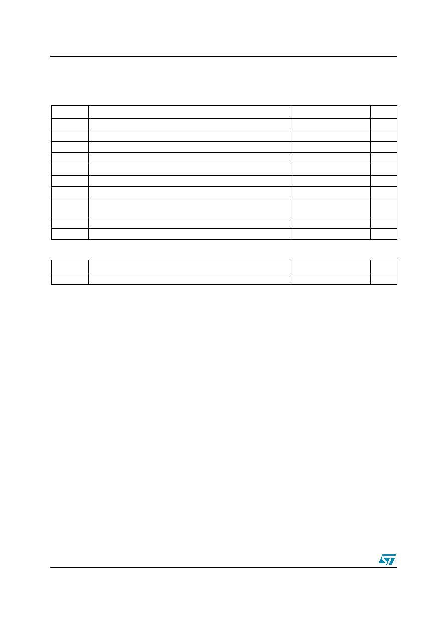
Internal schematic diagram
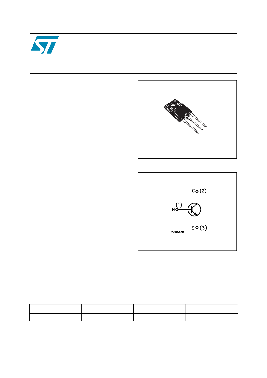
ISOWATT218FX
1
2
3
www.st.com
Order codes
Part Number
Marking
Package
Packing
ST8812FX
ST8812FX
ISOWATT218FX
TUBE
Electrical ratings
ST8812FX
2/10
1 Electrical
ratings
Table 1.
Absolute maximum rating
Table 2.
Thermal data
Symbol
Parameter
Value
Unit
V
CBO
Collector-Base Voltage (I
E
= 0)
1150
V
V
CEO
Collector-Emitter Voltage (I
B
= 0)
600
V
V
EBO
Emitte-Base Voltage (I
C
= 0)
15
V
I
C
Collector Current
7
A
I
CM
Collector Peak Current (t
P
< 5ms)
12
A
I
B
Base Current
4
A
P
TOT
Total dissipation at T
c
= 25∞C
50
W
V
isol
Insulation Withstand Voltage (RMS) from All Three Leads to
External Heatsink
2500
V
T
STG
Storage Temperature
-65 to 150
∞C
T
J
Max. Operating Junction Temperature
150
∞C
Symbol
Parameter
Value
Unit
R
thJ-case
Thermal Resistance Junction-Case
__________________ __
Max
2.5
∞C/W
ST8812FX
Electrical characteristics
3/10
2 Electrical
characteristics
(T
CASE
= 25∞C; unless otherwise specified)
Table 3.
Electrical characteristics
Note: 1 Pulsed duration = 300
µ
s, duty cycle
1.5%.
Symbol
Parameter
Test Conditions
Min.
Typ.
Max.
Unit
I
CES
Collector Cut-off Current
(V
BE
= 0)
V
CE
= 1150V
V
CE
= 1150V T
c
= 125∞C
1
2
mA
mA
I
EBO
Emitter Cut-off Current
(I
C
= 0)
V
EB
= 14V
1
mA
V
CEO(sus)
Note: 1
Collector-Emitter
Sustaining Voltage (I
B
= 0)
I
C
= 100mA
600
V
V
CE(sat)
Note: 1
Collector-Emitter Saturation Voltage
I
C
= 4A
_____
I
B
= 0.8A
I
C
= 4A
___ __
I
B
= 1.2A
3
1.5
V
V
V
BE(sat)
Note: 1
Base-Emitter Saturation Voltage
I
C
= 4A
____ _
I
B
= 0.8A
1.3
V
h
FE
DC Current Gain
I
C
= 1A
_____
V
CE
= 5V
I
C
= 5A
_____
V
CE
= 1V
I
C
= 5A
_____
V
CE
= 5V
4.5
25
5
9
t
s
t
f
INDUCTIVE LOAD
Storage Time
Fall Time
I
C
= 4A
____ _
R
BB
= 0
V
Clamp
= 480V V
BE(off)
= -5V
I
B1
= 0.8A
_
L
C
= 220
µ
H
(See
Figure 8
)
1
60
1.6
120
µ
s
ns
Electrical characteristics
ST8812FX
4/10
2.1
Typical characteristics test circuit
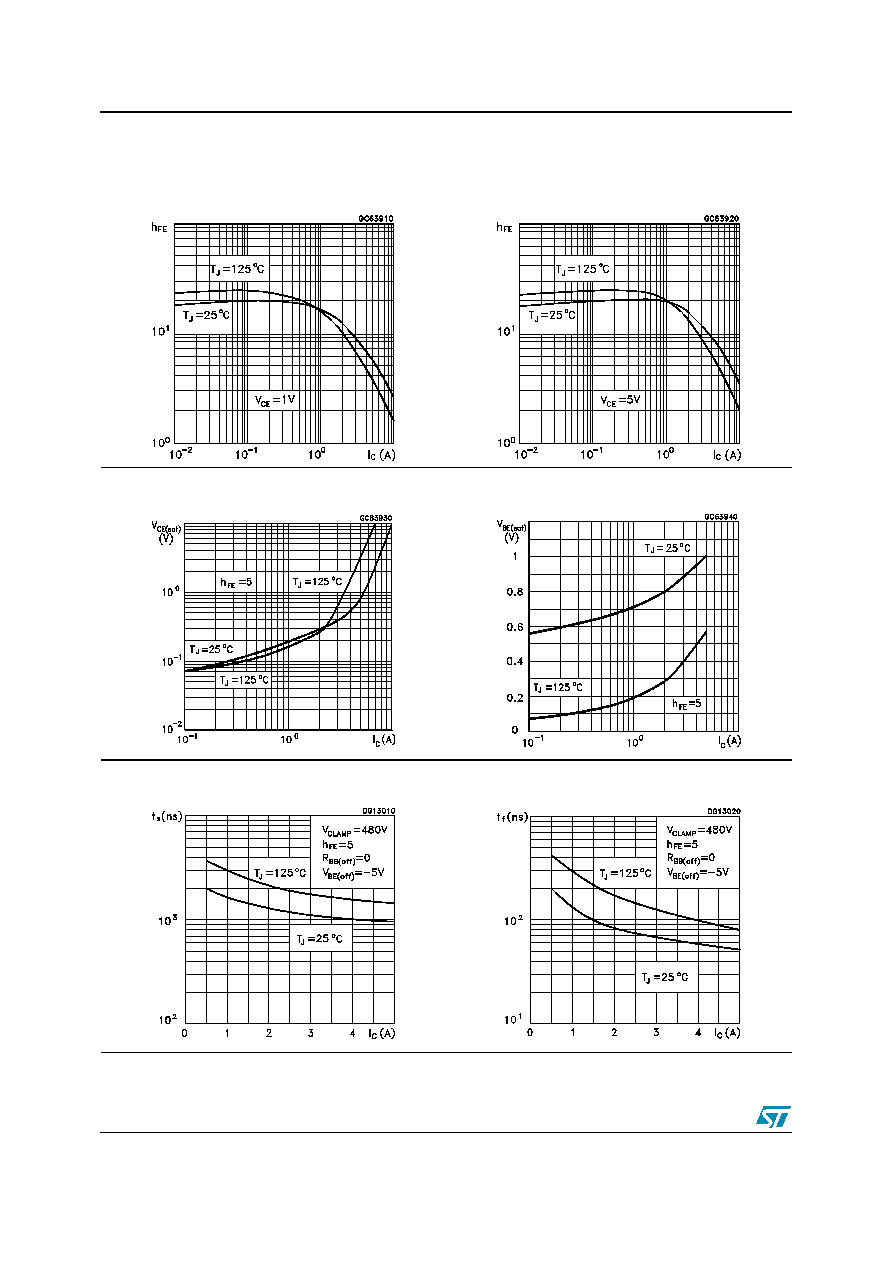
Figure 1.
DC current gain
Figure 2.
DC current gain
Figure 3.
Collector emitter saturation voltage Figure 4.
Base emitter saturation voltage
Figure 5.
Inductive load storage time
Figure 6.
Inductive load fall time
ST8812FX
Electrical characteristics
5/10
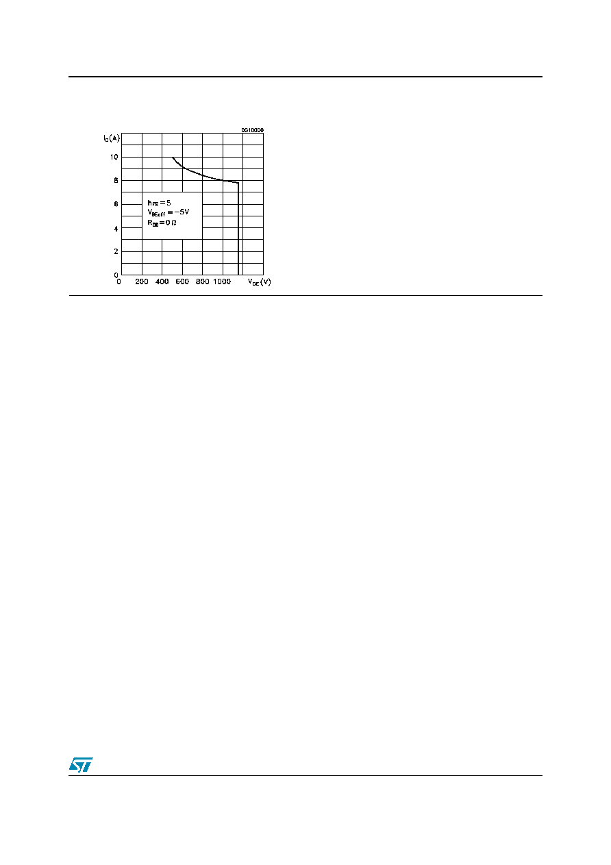
Figure 7.
Reverse biased S.O.A.