 | –≠–ª–µ–∫—Ç—Ä–æ–Ω–Ω—ã–π –∫–æ–º–ø–æ–Ω–µ–Ω—Ç: ST9040 | –°–∫–∞—á–∞—Ç—å:  PDF PDF  ZIP ZIP |
ST9040
Æ
February 1997
16K ROM HCMOS MCU
WITH EEPROM, RAM AND A/D CONVERTER
(Ordering Information at the end of the Datasheet)
PQFP80
PLCC68
Register oriented 8/16 bit CORE with
RUN, WFI and HALT modes
Minimum instruction cycle time : 500ns
(12MHz internal)
Internal Memory :
ROM
16K bytes
RAM
256 bytes
EEPROM
512 bytes
224 general purpose registers available as RAM,
accumulators or index registers (register file)
80-pin PQFP package for ST9040Q
68-lead PLCC package for ST9040C
DMA controller, Interrupt handler and Serial Pe-
ripheral Interface as standard features
Up to 56 fully programmable I/O pins
Up to 8 external plus 1 non-maskableinterrupts
16 bit Timer with 8 bit Prescaler, able to be used
as a Watchdog Timer
Two 16 bit Multifunction Timers, each with an 8
bit prescaler and 13 operating modes
8 channel 8 bit Analog to Digital Converter, with
Analog Watchdogs and external references
Serial Communications Interface with asynchro-
nous and synchronous capability
Rich Instruction Set and 14 Addressingmodes
Division-by-Zero trap generation
Versatile development tools, including assembler,
linker, C-compiler, archiver, graphic oriented de-
buggerand hardware emulators
Real Time Operating System
Windowed and One Time Programmable EPROM
parts available for prototyping and pre-production
developmentphases
Pin to pin compatible with ST9036
1/56

TABLE OF CONTENTS
ST9040
. . . . . . . . . . . . . . . . . . . . . . . . . . . . . . . . . . . . . . . . . . . . .
1
1.1 GENERAL DESCRIPTION
. . . . . . . . . . . . . . . . . . . . . . . . . . . . . .
5
1.2 PIN DESCRIPTION . . . . . . . . . . . . . . . . . . . . . . . . . . . . . . . . . .
6
1.2.1 I/O Port Alternate Functions . . . . . . . . . . . . . . . . . . . . . . . . .
6
1.3
MEMORY . . . . . . . . . . . . . . . . . . . . . . . . . . . . . . . . . . . . . .
10
1.3.1 INTRODUCTION . . . . . . . . . . . . . . . . . . . . . . . . . . . . . . .
10
1.3.2 EEPROM . . . . . . . . . . . . . . . . . . . . . . . . . . . . . . . . . . .
10
1.3.2.1 Introduction . . . . . . . . . . . . . . . . . . . . . . . . . . . . . .
10
1.3.2.2 EEPROM Programming Procedure . . . . . . . . . . . . . . . . . .
11
1.3.2.3 Parallel Programming Procedure . . . . . . . . . . . . . . . . . . .
11
1.3.2.4 EEPROM Programming Voltage
. . . . . . . . . . . . . . . . . . .
11
1.3.2.5 EEPROM Programming Time . . . . . . . . . . . . . . . . . . . . .
11
1.3.2.6 EEPROM Interrupt Management . . . . . . . . . . . . . . . . . . .
11
1.3.2.7 EEPROM Control Register . . . . . . . . . . . . . . . . . . . . . .
12
1.3.3 REGISTER MAP . . . . . . . . . . . . . . . . . . . . . . . . . . . . . . .
12
2
ELECTRICAL CHARACTERISTICS
. . . . . . . . . . . . . . . . . . . . . . . . . . . . . .
13
ST90E40 / ST90T40
. . . . . . . . . . . . . . . . . . . . . . . . . . . . . . . . . . .
35
1.1 GENERAL DESCRIPTION . . . . . . . . . . . . . . . . . . . . . . . . . . . . . .
38
1.2 PIN DESCRIPTION . . . . . . . . . . . . . . . . . . . . . . . . . . . . . . . . . .
39
1.2.1 I/O PORT ALTERNATE FUNCTIONS . . . . . . . . . . . . . . . . . . . .
39
1.1 MEMORY . . . . . . . . . . . . . . . . . . . . . . . . . . . . . . . . . . . . . . .
42
1.2 EPROM PROGRAMMING
. . . . . . . . . . . . . . . . . . . . . . . . . . . . . .
42
1.2.1 Eprom Erasing . . . . . . . . . . . . . . . . . . . . . . . . . . . . . . . .
42
ST90R40
. . . . . . . . . . . . . . . . . . . . . . . . . . . . . . . . . . . . . . . . . . . .
49
1.1 GENERAL DESCRIPTION . . . . . . . . . . . . . . . . . . . . . . . . . . . . . .
51
1.2 PIN DESCRIPTION . . . . . . . . . . . . . . . . . . . . . . . . . . . . . . . . . .
52
1.2.1 I/O PORT ALTERNATE FUNCTIONS . . . . . . . . . . . . . . . . . . . .
52
1.3 MEMORY . . . . . . . . . . . . . . . . . . . . . . . . . . . . . . . . . . . . . . .
55
Æ
2/56
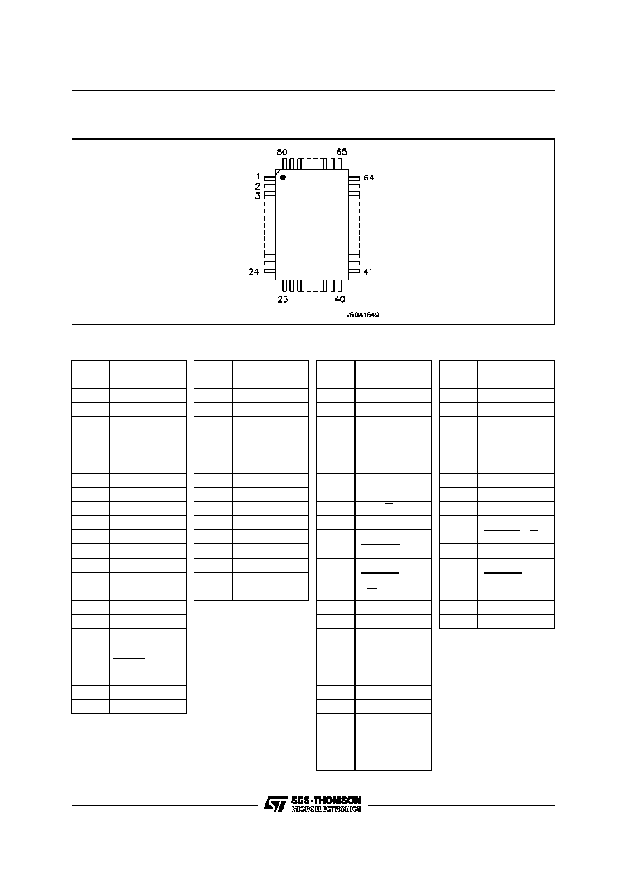
Figure 1. 80 Pin PQFP Package
Pin
Name
Pin
Name
Pin
Name
Pin
Name
1
AV
SS
25
P34/T1INA
64
P20/NMI
80
AV
DD
2
NC
26
P33/T0OUTB
63
NC
79
NC
3
NC
27
P32/T0INB
62
V
SS
78
P47/AIN7
4
P44/AIN4
28
P31/T0OUTA
61
P70/SIN
77
P46/AIN6
5
P57
29
P30/P/D/T0INA
60
P71/SOUT
76
P45/AIN5
6
P56
30
A15
59
P72/INT4/TXCLK
/CLKOUT
75
P43/AIN3
7
P55
31
A14
74
P42/AIN2
8
P54
32
NC
58
P73/INT5
/RXCLK/ADTRG
73
P41/AIN1
9
INT7
33
A13
72
P40/AIN0
10
INT0
34
A12
57
P74/P/D/INT6
71
P27/RRDY5
11
P53
35
A11
56
P75/WAIT
70
P26/INT3
/RDSTB5/P/D
12
NC
36
A10
55
P76/WDOUT
/BUSREQ
13
P52
37
A9
69
P25/WRRDY5
14
P51
38
A8
54
P77/WDIN
/BUSACK
68
P24/INT1
/WRSTB5
15
P50
39
P00/A0/D0
16
OSCOUT
40
P01/A1/D1
53
R/W
67
P23/SDO
17
V
SS
52
NC
66
P22/INT2/SCK
18
V
SS
51
DS
65
P21/SDI/P/D
19
NC
50
AS
20
OSCIN
49
NC
21
RESET
48
V
DD
22
P37/T1OUTB
47
V
DD
23
P36/T1INB
46
P07/A7/D7
24
P35/T1OUTA
45
P06/A6/D6
44
P05/A5/D5
43
P04/A4/D4
42
P03/A3/D3
41
P02/A2/D2
Table 1. ST9040Q Pin Description
Æ
ST9040
3/56
Pin
Name
Pin
Name
Pin
Name
Pin
Name
61
P44/AIN4
10
P35/T1OUTA
43
P70/SIN
60
AV
SS
62
P57
11
P34/T1INA
42
P71/SOUT
59
AV
DD
63
P56
12
P33/T0OUTB
41
P72/CLKOUT
/TXCLK/INT4
58
P47/AIN7
64
P55
13
P32/T0INB
57
P46/AIN6
65
P54
14
P31/T0OUTA
40
P73/ADTRG
/RXCLK/INT5
56
P45/AIN5
66
INT7
15
P30/P/D/T0INA
55
P43/AIN3
67
INT0
16
P17/A15
39
P74/P/D/INT6
54
P42/AIN2
68
P53
17
P16/A14
38
P75/WAIT
53
P41/AIN1
q
1
P52
18
P15/A13
37
P76/WDOUT
/BUSREQ
52
P40/AIN0
2
P51
19
P14/A12
51
P27/RRDY5
3
P50
20
P13/A11
36
P77/WDIN
/BUSACK
50
P26/INT3
/RDSTB5/P/D
4
OSCOUT
21
P12/A10
5
V
SS
22
P11/A9
35
R/W
49
P25/WRRDY5
6
OSCIN
23
P10/A8
34
DS
48
P24/INT1
/WRSTB5
7
RESET
24
P00/A0/D0
33
AS
8
P37/T1OUTB
25
P01/A1/D1
32
V
DD
47
P23/SDO
9
P36/T1INB
26
P02/A2/D2
31
P07/A7/D7
46
P22/INT2/SCK
30
P06/A6/D6
45
P21/SDI/P/D
29
P05/A5/D5
44
P20/NMI
28
P04/A4/D4
27
P03/A3/D3
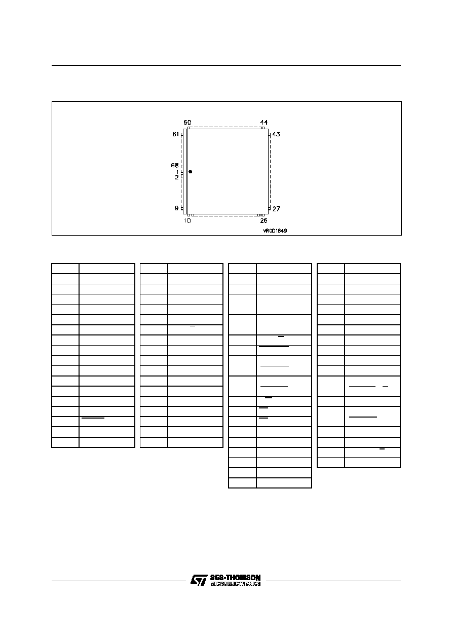
Table 2. ST9040C Pin Description
Figure 2. 68 Pin PLCC Package
Æ
ST9040
4/56

1.1GENERAL DESCRIPTION
The ST9040 is a ROM member of the ST9 family of
microcontrollers, completely developed and pro-
duced by SGS-THOMSON Microelectronics using
a proprietary n-well HCMOS process.
The ST9040 peripheral and functional actions are
fully compatible throughout the ST903x/4x family.
This datasheet will thus provide only information
specific to this ROM device.
THE READER IS ASKED TO REFER TO THE
DATASHEET OF THE ST9036 ROM-BASED DE-
VICE FOR FURTHER DETAILS.
The nucleus of the ST9040 is the advanced Core
which includes the Central Processing Unit (CPU),
the Register File, a 16 bit Timer/Watchdog with 8
bit Prescaler, a Serial Peripheral Interface support-
ing S-bus, I
2
C-bus and IM-bus Interface, plus two 8
bit I/O ports. The Core has independent memory
and register buses allowing a high degree of pipe-
lining to add to the efficiency of the code execution
speed of the extensive instruction set. The power-
ful I/O capabilities demanded by microcontroller
applications are fulfilled by the ST9040 with up to
56 I/O lines dedicated to digital Input/Output.
These lines are grouped into up to seven 8 bit I/O
Ports and can be configured on a bit basis under
software control to provide timing, status signals,
an address/data bus for interfacing external mem-
ory, timer inputs and outputs, analog inputs, exter-
nal interrupts and serial or parallel I/O with or
without handshake.
Three basic memory spaces are available to support
this wide range of configurations: Program Memory
(internal and external), Data Memory (internal and ex-
ternal)andtheRegisterFile, which includesthecontrol
and status registers of theon-chip peripherals.
Two 16 bit MultiFunction Timers, each with an 8 bit
Prescaler and 13 operating modes allow simple
use for complex waveform generation and meas-
urement, PWM functions and many other system
timing functionsby the usage of the two associated
DMA channels for each timer. In addition there is
an 8 channel Analog to Digital Converter with inte-
gral sample and hold, fast 11
µ
s conversion time
and 8 bit resolution. An Analog Watchdog feature
is included for two input channels.
Completing the device is a full duplex Serial Com-
munications Interface with an integral 110 to
375,000 baud rate generator, asynchronous and
1.5Mbyte/s synchronous capability (fully program-
mable format) and associated address/wake-up
option, plus two DMA channels.
Æ
ST9040
5/56