 | –≠–ª–µ–∫—Ç—Ä–æ–Ω–Ω—ã–π –∫–æ–º–ø–æ–Ω–µ–Ω—Ç: ST92163V1 | –°–∫–∞—á–∞—Ç—å:  PDF PDF  ZIP ZIP |
January 2002
1/230
ST92163
8/16-BIT FULL SPEED USB MCU FOR COMPOSITE DEVICES
WITH 16 ENDPOINTS, 20K ROM, 2K RAM, I
2
C, SCI, & MFT
DATASHEET
s
Internal Memories: 20 Kbytes ROM/EPROM/
OTP, 2 Kbytes RAM
s
Register oriented 8/16 bit core
s
224 general purpose registers available as
RAM, accumulators or index pointers
s
Minimum instruction cycle time: 167 ns (@24
MHz CPU frequency)
s
Low power modes: WFI, SLOW, HALT and
STOP
s
DMA controller for reduced processor overhead
s
Full speed USB interface with DMA, compliant
with USB specifications version 1.1 (in normal
voltage mode)
s
USB Embedded Functions with 16 fully
configurable endpoints (buffer size
programmable), supporting all USB data
transfer types (Isochronous included)
s
On-chip USB transceiver and 3.3 voltage
regulator
s
Multimaster I
2
C-bus serial interface up to
400KHz. with DMA capability
s
Serial Communications Interface (SCI) with
DMA capability:
≠ Asynchronous mode up to 315 Kb/s
≠ Synchronous mode up to 6 MHz
s
External memory interface (8-bit data/16-bit
address) with DMA capability from the USB
s
16-bit Multi-Function Timer (12 operating
modes) with DMA capability
s
16-bit Timer with 8-bit prescaler and Watchdog
s
6-channel, 8-bit A/D Converter (ADC)
s
15 interrupt pins on 8 interrupt channels
s
14 pins programmable as wake-up or additional
external interrupts
s
44 fully programmable I/Os with 6 or 8 high sink
pads (10 mA @ 1 V)
s
Programmable PLL clock generator (RCCU)
using a low frequency external quartz (8 MHz)
s
On-chip RC oscillator for low power operation
s
Low Voltage Detector Reset on some devices
1
s
Rich instruction set with 14 addressing modes
s
Several operating voltage modes available on
some devices
1
:
≠ Normal Voltage Mode
≠ 8-MHz Low Voltage Mode
≠ 16-MHz Low Voltage Mode
s
0 - 24 MHz CPU clock operation @ 4.0-5.5 V (all
devices)
s
0 - 8 MHz CPU clock operation @ 3.0-4.0 V (8-
MHz and 16-MHz Low Voltage devices)
s
0 - 16 MHz CPU clock operation @ 3.0-4.0 V
(16-MHz Low Voltage devices only)
s
Division-by-zero trap generation
s
0
o
C to 70
o
C temperature range
s
Low EMI design supporting single sided PCB
s
Complete development tools, including
assembler, linker, C-compiler, archiver, source
level debugger and hardware emulators, and
Real Time Operating System
Note 1: Refer to "Device Summary" on page 6
1
TQFP64
Rev. 2.4

2/230
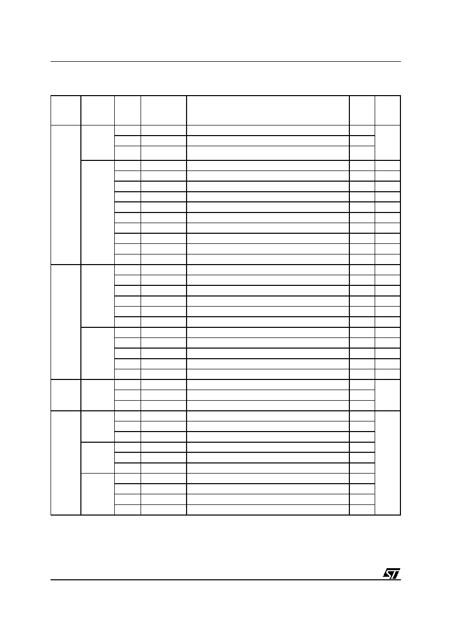
Table of Contents
ST92163 . . . . . . . . . . . . . . . . . . . . . . . . . . . . . . . . . . . . . . . . . . . . 1
1 GENERAL DESCRIPTION . . . . . . . . . . . . . . . . . . . . . . . . . . . . . . . . . . . . . . . . . . . . . . . . . . . . . . 6
1.1 INTRODUCTION . . . . . . . . . . . . . . . . . . . . . . . . . . . . . . . . . . . . . . . . . . . . . . . . . . . . . . . . . 6
1.1.1
Core Architecture . . . . . . . . . . . . . . . . . . . . . . . . . . . . . . . . . . . . . . . . . . . . . . . . . . . 9
1.1.2
Instruction Set . . . . . . . . . . . . . . . . . . . . . . . . . . . . . . . . . . . . . . . . . . . . . . . . . . . . . . 9
1.1.3
External MEMORY INTERFACE . . . . . . . . . . . . . . . . . . . . . . . . . . . . . . . . . . . . . . . 9
1.1.4
OPERATING MODES . . . . . . . . . . . . . . . . . . . . . . . . . . . . . . . . . . . . . . . . . . . . . . . 9
1.1.5
On-chip Peripherals . . . . . . . . . . . . . . . . . . . . . . . . . . . . . . . . . . . . . . . . . . . . . . . . 10
1.2 PIN DESCRIPTION . . . . . . . . . . . . . . . . . . . . . . . . . . . . . . . . . . . . . . . . . . . . . . . . . . . . . . 11
1.3 I/O PORT PINS . . . . . . . . . . . . . . . . . . . . . . . . . . . . . . . . . . . . . . . . . . . . . . . . . . . . . . . . . 13
1.4 MEMORY MAP . . . . . . . . . . . . . . . . . . . . . . . . . . . . . . . . . . . . . . . . . . . . . . . . . . . . . . . . . 19
1.5 ST92163 REGISTER MAP . . . . . . . . . . . . . . . . . . . . . . . . . . . . . . . . . . . . . . . . . . . . . . . . 20
2 DEVICE ARCHITECTURE . . . . . . . . . . . . . . . . . . . . . . . . . . . . . . . . . . . . . . . . . . . . . . . . . . . . . 27
2.1 CORE ARCHITECTURE . . . . . . . . . . . . . . . . . . . . . . . . . . . . . . . . . . . . . . . . . . . . . . . . . . 27
2.2 MEMORY SPACES . . . . . . . . . . . . . . . . . . . . . . . . . . . . . . . . . . . . . . . . . . . . . . . . . . . . . . 27
2.2.1
Register File . . . . . . . . . . . . . . . . . . . . . . . . . . . . . . . . . . . . . . . . . . . . . . . . . . . . . . 27
2.2.2
Register Addressing . . . . . . . . . . . . . . . . . . . . . . . . . . . . . . . . . . . . . . . . . . . . . . . . 29
2.3 SYSTEM REGISTERS . . . . . . . . . . . . . . . . . . . . . . . . . . . . . . . . . . . . . . . . . . . . . . . . . . . . 30
2.3.1
Central Interrupt Control Register . . . . . . . . . . . . . . . . . . . . . . . . . . . . . . . . . . . . . . 30
2.3.2
Flag Register . . . . . . . . . . . . . . . . . . . . . . . . . . . . . . . . . . . . . . . . . . . . . . . . . . . . . 31
2.3.3
Register Pointing Techniques . . . . . . . . . . . . . . . . . . . . . . . . . . . . . . . . . . . . . . . . . 32
2.3.4
Paged Registers . . . . . . . . . . . . . . . . . . . . . . . . . . . . . . . . . . . . . . . . . . . . . . . . . . . 35
2.3.5
Mode Register . . . . . . . . . . . . . . . . . . . . . . . . . . . . . . . . . . . . . . . . . . . . . . . . . . . . 35
2.3.6
Stack Pointers . . . . . . . . . . . . . . . . . . . . . . . . . . . . . . . . . . . . . . . . . . . . . . . . . . . . . 36
2.4 MEMORY ORGANIZATION . . . . . . . . . . . . . . . . . . . . . . . . . . . . . . . . . . . . . . . . . . . . . . . . 38
2.5 MEMORY MANAGEMENT UNIT . . . . . . . . . . . . . . . . . . . . . . . . . . . . . . . . . . . . . . . . . . . . 39
2.6 ADDRESS SPACE EXTENSION . . . . . . . . . . . . . . . . . . . . . . . . . . . . . . . . . . . . . . . . . . . . 40
2.6.1
Addressing 16-Kbyte Pages . . . . . . . . . . . . . . . . . . . . . . . . . . . . . . . . . . . . . . . . . . 40
2.6.2
Addressing 64-Kbyte Segments . . . . . . . . . . . . . . . . . . . . . . . . . . . . . . . . . . . . . . . 41
2.7 MMU REGISTERS . . . . . . . . . . . . . . . . . . . . . . . . . . . . . . . . . . . . . . . . . . . . . . . . . . . . . . . 41
2.7.1
DPR[3:0]: Data Page Registers . . . . . . . . . . . . . . . . . . . . . . . . . . . . . . . . . . . . . . . 41
2.7.2
CSR: Code Segment Register . . . . . . . . . . . . . . . . . . . . . . . . . . . . . . . . . . . . . . . . 43
2.7.3
ISR: Interrupt Segment Register . . . . . . . . . . . . . . . . . . . . . . . . . . . . . . . . . . . . . . . 43
2.7.4
DMASR: DMA Segment Register . . . . . . . . . . . . . . . . . . . . . . . . . . . . . . . . . . . . . . 43
2.8 MMU USAGE . . . . . . . . . . . . . . . . . . . . . . . . . . . . . . . . . . . . . . . . . . . . . . . . . . . . . . . . . . . 45
2.8.1
Normal Program Execution . . . . . . . . . . . . . . . . . . . . . . . . . . . . . . . . . . . . . . . . . . . 45
2.8.2
Interrupts . . . . . . . . . . . . . . . . . . . . . . . . . . . . . . . . . . . . . . . . . . . . . . . . . . . . . . . . . 45
2.8.3
DMA . . . . . . . . . . . . . . . . . . . . . . . . . . . . . . . . . . . . . . . . . . . . . . . . . . . . . . . . . . . . 45
3 INTERRUPTS . . . . . . . . . . . . . . . . . . . . . . . . . . . . . . . . . . . . . . . . . . . . . . . . . . . . . . . . . . . . . . . 46
3.1 INTRODUCTION . . . . . . . . . . . . . . . . . . . . . . . . . . . . . . . . . . . . . . . . . . . . . . . . . . . . . . . . 46
3.2 INTERRUPT VECTORING . . . . . . . . . . . . . . . . . . . . . . . . . . . . . . . . . . . . . . . . . . . . . . . . 47
3.2.1
Divide by Zero trap . . . . . . . . . . . . . . . . . . . . . . . . . . . . . . . . . . . . . . . . . . . . . . . . . 47
3.2.2
Segment Paging During Interrupt Routines . . . . . . . . . . . . . . . . . . . . . . . . . . . . . . 48
3.3 INTERRUPT PRIORITY LEVELS . . . . . . . . . . . . . . . . . . . . . . . . . . . . . . . . . . . . . . . . . . . 48

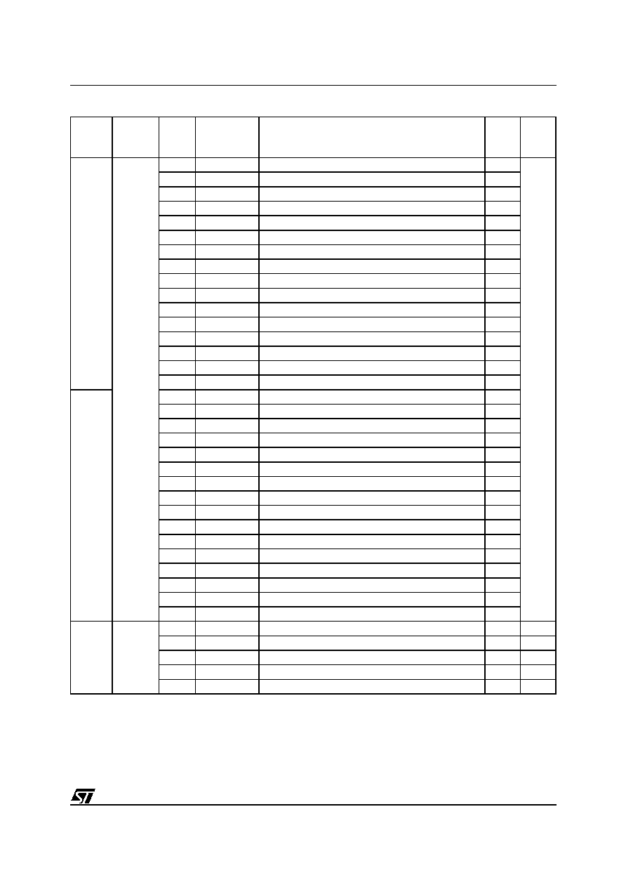
3/230
Table of Contents
230
3.4 PRIORITY LEVEL ARBITRATION . . . . . . . . . . . . . . . . . . . . . . . . . . . . . . . . . . . . . . . . . . . 48
3.4.1
Priority Level 7 (Lowest) . . . . . . . . . . . . . . . . . . . . . . . . . . . . . . . . . . . . . . . . . . . . . 48
3.4.2
Maximum Depth of Nesting . . . . . . . . . . . . . . . . . . . . . . . . . . . . . . . . . . . . . . . . . . 48
3.4.3
Simultaneous Interrupts . . . . . . . . . . . . . . . . . . . . . . . . . . . . . . . . . . . . . . . . . . . . . 48
3.4.4
Dynamic Priority Level Modification . . . . . . . . . . . . . . . . . . . . . . . . . . . . . . . . . . . . 49
3.5 ARBITRATION MODES . . . . . . . . . . . . . . . . . . . . . . . . . . . . . . . . . . . . . . . . . . . . . . . . . . . 49
3.5.1
Concurrent Mode . . . . . . . . . . . . . . . . . . . . . . . . . . . . . . . . . . . . . . . . . . . . . . . . . . 49
3.5.2
Nested Mode . . . . . . . . . . . . . . . . . . . . . . . . . . . . . . . . . . . . . . . . . . . . . . . . . . . . . 52
3.6 EXTERNAL INTERRUPTS . . . . . . . . . . . . . . . . . . . . . . . . . . . . . . . . . . . . . . . . . . . . . . . . 54
3.7 MANAGEMENT OF WAKE-UP LINES AND EXTERNAL INTERRUPT LINES . . . . . . . . . 56
3.8 TOP LEVEL INTERRUPT . . . . . . . . . . . . . . . . . . . . . . . . . . . . . . . . . . . . . . . . . . . . . . . . . 57
3.9 ON-CHIP PERIPHERAL INTERRUPTS . . . . . . . . . . . . . . . . . . . . . . . . . . . . . . . . . . . . . . 57
3.10 INTERRUPT RESPONSE TIME . . . . . . . . . . . . . . . . . . . . . . . . . . . . . . . . . . . . . . . . . . . . 58
3.11 INTERRUPT REGISTERS . . . . . . . . . . . . . . . . . . . . . . . . . . . . . . . . . . . . . . . . . . . . . . . . . 59
3.12 WAKE-UP / INTERRUPT LINES MANAGEMENT UNIT (WUIMU) . . . . . . . . . . . . . . . . . . 63
3.12.1 Introduction . . . . . . . . . . . . . . . . . . . . . . . . . . . . . . . . . . . . . . . . . . . . . . . . . . . . . . . 63
3.12.2 Main Features . . . . . . . . . . . . . . . . . . . . . . . . . . . . . . . . . . . . . . . . . . . . . . . . . . . . . 63
3.12.3 Functional Description . . . . . . . . . . . . . . . . . . . . . . . . . . . . . . . . . . . . . . . . . . . . . . 64
3.12.4 Programming Considerations . . . . . . . . . . . . . . . . . . . . . . . . . . . . . . . . . . . . . . . . . 66
3.12.5 Register Description . . . . . . . . . . . . . . . . . . . . . . . . . . . . . . . . . . . . . . . . . . . . . . . . 67
4 ON-CHIP DIRECT MEMORY ACCESS (DMA) . . . . . . . . . . . . . . . . . . . . . . . . . . . . . . . . . . . . . . 70
4.1 INTRODUCTION . . . . . . . . . . . . . . . . . . . . . . . . . . . . . . . . . . . . . . . . . . . . . . . . . . . . . . . . 70
4.2 DMA PRIORITY LEVELS . . . . . . . . . . . . . . . . . . . . . . . . . . . . . . . . . . . . . . . . . . . . . . . . . . 70
4.3 DMA TRANSACTIONS . . . . . . . . . . . . . . . . . . . . . . . . . . . . . . . . . . . . . . . . . . . . . . . . . . . 71
4.4 DMA CYCLE TIME . . . . . . . . . . . . . . . . . . . . . . . . . . . . . . . . . . . . . . . . . . . . . . . . . . . . . . . 73
4.5 SWAP MODE . . . . . . . . . . . . . . . . . . . . . . . . . . . . . . . . . . . . . . . . . . . . . . . . . . . . . . . . . . . 73
4.6 DMA REGISTERS . . . . . . . . . . . . . . . . . . . . . . . . . . . . . . . . . . . . . . . . . . . . . . . . . . . . . . . 74
5 RESET AND CLOCK CONTROL UNIT (RCCU) . . . . . . . . . . . . . . . . . . . . . . . . . . . . . . . . . . . . 75
5.1 INTRODUCTION . . . . . . . . . . . . . . . . . . . . . . . . . . . . . . . . . . . . . . . . . . . . . . . . . . . . . . . . 75
5.2 CLOCK CONTROL UNIT . . . . . . . . . . . . . . . . . . . . . . . . . . . . . . . . . . . . . . . . . . . . . . . . . . 75
5.2.1
Clock Control Unit Overview . . . . . . . . . . . . . . . . . . . . . . . . . . . . . . . . . . . . . . . . . . 75
5.3 CLOCK MANAGEMENT . . . . . . . . . . . . . . . . . . . . . . . . . . . . . . . . . . . . . . . . . . . . . . . . . . 77
5.3.1
PLL Clock Multiplier Programming . . . . . . . . . . . . . . . . . . . . . . . . . . . . . . . . . . . . . 78
5.3.2
CPU Clock Prescaling . . . . . . . . . . . . . . . . . . . . . . . . . . . . . . . . . . . . . . . . . . . . . . 78
5.3.3
Peripheral Clock . . . . . . . . . . . . . . . . . . . . . . . . . . . . . . . . . . . . . . . . . . . . . . . . . . . 78
5.3.4
Low Power Modes . . . . . . . . . . . . . . . . . . . . . . . . . . . . . . . . . . . . . . . . . . . . . . . . . 79
5.3.5
Interrupt Generation . . . . . . . . . . . . . . . . . . . . . . . . . . . . . . . . . . . . . . . . . . . . . . . . 79
5.4 CLOCK CONTROL REGISTERS . . . . . . . . . . . . . . . . . . . . . . . . . . . . . . . . . . . . . . . . . . . . 81
5.5 OSCILLATOR CHARACTERISTICS . . . . . . . . . . . . . . . . . . . . . . . . . . . . . . . . . . . . . . . . . 85
5.6 RESET/STOP MANAGER . . . . . . . . . . . . . . . . . . . . . . . . . . . . . . . . . . . . . . . . . . . . . . . . . 86
5.6.1
RESET Pin Timing . . . . . . . . . . . . . . . . . . . . . . . . . . . . . . . . . . . . . . . . . . . . . . . . . 87
5.7 STOP MODE . . . . . . . . . . . . . . . . . . . . . . . . . . . . . . . . . . . . . . . . . . . . . . . . . . . . . . . . . . . 87
5.8 LOW VOLTAGE DETECTOR (LVD) RESET . . . . . . . . . . . . . . . . . . . . . . . . . . . . . . . . . . . 88
6 EXTERNAL MEMORY INTERFACE (EXTMI) . . . . . . . . . . . . . . . . . . . . . . . . . . . . . . . . . . . . . . 90

4/230
Table of Contents
6.1 INTRODUCTION . . . . . . . . . . . . . . . . . . . . . . . . . . . . . . . . . . . . . . . . . . . . . . . . . . . . . . . . 90
6.2 EXTERNAL MEMORY SIGNALS . . . . . . . . . . . . . . . . . . . . . . . . . . . . . . . . . . . . . . . . . . . . 91
6.2.1
AS: Address Strobe . . . . . . . . . . . . . . . . . . . . . . . . . . . . . . . . . . . . . . . . . . . . . . . . 91
6.2.2
DS: Data Strobe . . . . . . . . . . . . . . . . . . . . . . . . . . . . . . . . . . . . . . . . . . . . . . . . . . . 91
6.2.3
DS2: Data Strobe 2 . . . . . . . . . . . . . . . . . . . . . . . . . . . . . . . . . . . . . . . . . . . . . . . . . 91
6.2.4
RW: Read/Write . . . . . . . . . . . . . . . . . . . . . . . . . . . . . . . . . . . . . . . . . . . . . . . . . . . 94
6.2.5
BREQ, BACK: Bus Request, Bus Acknowledge . . . . . . . . . . . . . . . . . . . . . . . . . . . 94
6.2.6
PORT 0 . . . . . . . . . . . . . . . . . . . . . . . . . . . . . . . . . . . . . . . . . . . . . . . . . . . . . . . . . . 95
6.2.7
PORT 1 . . . . . . . . . . . . . . . . . . . . . . . . . . . . . . . . . . . . . . . . . . . . . . . . . . . . . . . . . . 95
6.2.8
WAIT: External Memory Wait . . . . . . . . . . . . . . . . . . . . . . . . . . . . . . . . . . . . . . . . . 95
6.3 REGISTER DESCRIPTION . . . . . . . . . . . . . . . . . . . . . . . . . . . . . . . . . . . . . . . . . . . . . . . . 96
7 I/O PORTS . . . . . . . . . . . . . . . . . . . . . . . . . . . . . . . . . . . . . . . . . . . . . . . . . . . . . . . . . . . . . . . . . . 99
7.1 INTRODUCTION . . . . . . . . . . . . . . . . . . . . . . . . . . . . . . . . . . . . . . . . . . . . . . . . . . . . . . . . 99
7.2 SPECIFIC PORT CONFIGURATIONS . . . . . . . . . . . . . . . . . . . . . . . . . . . . . . . . . . . . . . . 99
7.3 PORT CONTROL REGISTERS . . . . . . . . . . . . . . . . . . . . . . . . . . . . . . . . . . . . . . . . . . . . . 99
7.4 INPUT/OUTPUT BIT CONFIGURATION . . . . . . . . . . . . . . . . . . . . . . . . . . . . . . . . . . . . . 100
7.5 ALTERNATE FUNCTION ARCHITECTURE . . . . . . . . . . . . . . . . . . . . . . . . . . . . . . . . . . 104
7.5.1
Pin Declared as I/O . . . . . . . . . . . . . . . . . . . . . . . . . . . . . . . . . . . . . . . . . . . . . . . . 104
7.5.2
Pin Declared as an Alternate Function Input . . . . . . . . . . . . . . . . . . . . . . . . . . . . 104
7.5.3
Pin Declared as an Alternate Function Output . . . . . . . . . . . . . . . . . . . . . . . . . . . 104
7.6 I/O STATUS AFTER WFI, HALT AND RESET . . . . . . . . . . . . . . . . . . . . . . . . . . . . . . . . 104
8 ON-CHIP PERIPHERALS . . . . . . . . . . . . . . . . . . . . . . . . . . . . . . . . . . . . . . . . . . . . . . . . . . . . . 105
8.1 TIMER/WATCHDOG (WDT) . . . . . . . . . . . . . . . . . . . . . . . . . . . . . . . . . . . . . . . . . . . . . . 105
8.1.1
Introduction . . . . . . . . . . . . . . . . . . . . . . . . . . . . . . . . . . . . . . . . . . . . . . . . . . . . . . 1 05
8.1.2
Functional Description . . . . . . . . . . . . . . . . . . . . . . . . . . . . . . . . . . . . . . . . . . . . . 106
8.1.3
Watchdog Timer Operation . . . . . . . . . . . . . . . . . . . . . . . . . . . . . . . . . . . . . . . . . . 107
8.1.4
WDT Interrupts . . . . . . . . . . . . . . . . . . . . . . . . . . . . . . . . . . . . . . . . . . . . . . . . . . . 109
8.1.5
Register Description . . . . . . . . . . . . . . . . . . . . . . . . . . . . . . . . . . . . . . . . . . . . . . . 110
8.2 MULTIFUNCTION TIMER (MFT) . . . . . . . . . . . . . . . . . . . . . . . . . . . . . . . . . . . . . . . . . . . 112
8.2.1
Introduction . . . . . . . . . . . . . . . . . . . . . . . . . . . . . . . . . . . . . . . . . . . . . . . . . . . . . . 112
8.2.2
Functional Description . . . . . . . . . . . . . . . . . . . . . . . . . . . . . . . . . . . . . . . . . . . . . 114
8.2.3
Input Pin Assignment . . . . . . . . . . . . . . . . . . . . . . . . . . . . . . . . . . . . . . . . . . . . . . 117
8.2.4
Output Pin Assignment . . . . . . . . . . . . . . . . . . . . . . . . . . . . . . . . . . . . . . . . . . . . . 121
8.2.5
Interrupt and DMA . . . . . . . . . . . . . . . . . . . . . . . . . . . . . . . . . . . . . . . . . . . . . . . . 123
8.2.6
Register Description . . . . . . . . . . . . . . . . . . . . . . . . . . . . . . . . . . . . . . . . . . . . . . . 125
8.3 USB PERIPHERAL (USB) . . . . . . . . . . . . . . . . . . . . . . . . . . . . . . . . . . . . . . . . . . . . . . . . 136
8.3.1
Introduction . . . . . . . . . . . . . . . . . . . . . . . . . . . . . . . . . . . . . . . . . . . . . . . . . . . . . . 136
8.3.2
Main Features . . . . . . . . . . . . . . . . . . . . . . . . . . . . . . . . . . . . . . . . . . . . . . . . . . . . 136
8.3.3
Functional Description . . . . . . . . . . . . . . . . . . . . . . . . . . . . . . . . . . . . . . . . . . . . . 136
8.3.4
Register Description . . . . . . . . . . . . . . . . . . . . . . . . . . . . . . . . . . . . . . . . . . . . . . . 141
8.3.5
Register pages summary . . . . . . . . . . . . . . . . . . . . . . . . . . . . . . . . . . . . . . . . . . . 151
8.4 MULTIPROTOCOL SERIAL COMMUNICATIONS INTERFACE (SCI-M) . . . . . . . . . . . . 153
8.4.1
Introduction . . . . . . . . . . . . . . . . . . . . . . . . . . . . . . . . . . . . . . . . . . . . . . . . . . . . . . 153
8.4.2
Main Features . . . . . . . . . . . . . . . . . . . . . . . . . . . . . . . . . . . . . . . . . . . . . . . . . . . . 153
8.4.3
Functional Description . . . . . . . . . . . . . . . . . . . . . . . . . . . . . . . . . . . . . . . . . . . . . 154
8.4.4
SCI-M Operating Modes . . . . . . . . . . . . . . . . . . . . . . . . . . . . . . . . . . . . . . . . . . . . 155

5/230
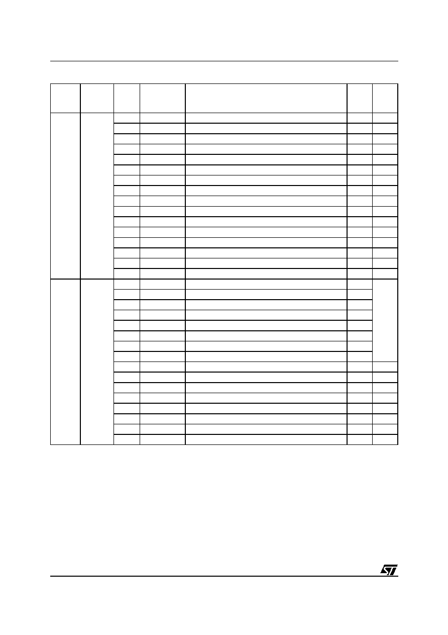
Table of Contents
230
8.4.5
Serial Frame Format . . . . . . . . . . . . . . . . . . . . . . . . . . . . . . . . . . . . . . . . . . . . . . . 158
8.4.6
Clocks And Serial Transmission Rates . . . . . . . . . . . . . . . . . . . . . . . . . . . . . . . . . 161
8.4.7
SCI -M Initialization Procedure . . . . . . . . . . . . . . . . . . . . . . . . . . . . . . . . . . . . . . . 161
8.4.8
Input Signals . . . . . . . . . . . . . . . . . . . . . . . . . . . . . . . . . . . . . . . . . . . . . . . . . . . . . 163
8.4.9
Output Signals . . . . . . . . . . . . . . . . . . . . . . . . . . . . . . . . . . . . . . . . . . . . . . . . . . . 163
8.4.10 Interrupts and DMA . . . . . . . . . . . . . . . . . . . . . . . . . . . . . . . . . . . . . . . . . . . . . . . . 164
8.4.11 Register Description . . . . . . . . . . . . . . . . . . . . . . . . . . . . . . . . . . . . . . . . . . . . . . . 167
8.5 I2C BUS INTERFACE . . . . . . . . . . . . . . . . . . . . . . . . . . . . . . . . . . . . . . . . . . . . . . . . . . . 178
8.5.1
Introduction . . . . . . . . . . . . . . . . . . . . . . . . . . . . . . . . . . . . . . . . . . . . . . . . . . . . . . 1 78
8.5.2
Main Features . . . . . . . . . . . . . . . . . . . . . . . . . . . . . . . . . . . . . . . . . . . . . . . . . . . . 178
8.5.3
Functional Description . . . . . . . . . . . . . . . . . . . . . . . . . . . . . . . . . . . . . . . . . . . . . 179
8.5.4
I2C State Machine . . . . . . . . . . . . . . . . . . . . . . . . . . . . . . . . . . . . . . . . . . . . . . . . 181
8.5.5
Interrupt Features . . . . . . . . . . . . . . . . . . . . . . . . . . . . . . . . . . . . . . . . . . . . . . . . . 186
8.5.6
DMA Features . . . . . . . . . . . . . . . . . . . . . . . . . . . . . . . . . . . . . . . . . . . . . . . . . . . . 187
8.5.7
Register Description . . . . . . . . . . . . . . . . . . . . . . . . . . . . . . . . . . . . . . . . . . . . . . . 189
8.6 A/D CONVERTER (A/D) . . . . . . . . . . . . . . . . . . . . . . . . . . . . . . . . . . . . . . . . . . . . . . . . . 200
8.6.1
Introduction . . . . . . . . . . . . . . . . . . . . . . . . . . . . . . . . . . . . . . . . . . . . . . . . . . . . . . 200
8.6.2
Main Features . . . . . . . . . . . . . . . . . . . . . . . . . . . . . . . . . . . . . . . . . . . . . . . . . . . . 200
8.6.3
General Description . . . . . . . . . . . . . . . . . . . . . . . . . . . . . . . . . . . . . . . . . . . . . . . 200
8.6.4
Register Description . . . . . . . . . . . . . . . . . . . . . . . . . . . . . . . . . . . . . . . . . . . . . . . 202
9 ELECTRICAL CHARACTERISTICS . . . . . . . . . . . . . . . . . . . . . . . . . . . . . . . . . . . . . . . . . . . . . 204
10 GENERAL INFORMATION . . . . . . . . . . . . . . . . . . . . . . . . . . . . . . . . . . . . . . . . . . . . . . . . . . . 223
10.1 EPROM/OTP PROGRAMMING . . . . . . . . . . . . . . . . . . . . . . . . . . . . . . . . . . . . . . . . . . . . 223
10.2 PACKAGE DESCRIPTION . . . . . . . . . . . . . . . . . . . . . . . . . . . . . . . . . . . . . . . . . . . . . . . 224
10.3 ORDERING INFORMATION . . . . . . . . . . . . . . . . . . . . . . . . . . . . . . . . . . . . . . . . . . . . . . 226
10.4 TRANSFER OF CUSTOMER CODE . . . . . . . . . . . . . . . . . . . . . . . . . . . . . . . . . . . . . . . . 226
11 SUMMARY OF CHANGES . . . . . . . . . . . . . . . . . . . . . . . . . . . . . . . . . . . . . . . . . . . . . . . . . . 229
6/230
ST92163 - GENERAL DESCRIPTION
1 GENERAL DESCRIPTION
1.1 INTRODUCTION
The ST9216x family brings the enhanced ST9 reg-
ister-based architecture to a new range of high-
performance microcontrollers specifically de-
signed for USB (Universal Serial Bus) applica-
tions. Their performance derives from the use of a
flexible 256-register programming model for ultra-
fast context switching and real-time event re-
sponse. The intelligent on-chip peripherals offload
the ST9 core from I/O and data management
processing tasks allowing critical application tasks
to get the maximum use of core resources. The
ST9 MCU devices support low power consumption
and low voltage operation for power-efficient and
low-cost embedded systems. In the ST92163 fam-
ily, four different types of device are available:
Normal Voltage Devices with LVD function
They operate in Normal Voltage Mode only (4.0-
5.5V @ 24MHz) and include the Low Voltage De-
tector (LVD) function.
Normal Voltage Devices without LVD function
They operate in Normal Voltage Mode only (4.0-
5.5V @ 24MHz) and do not include the Low Volt-
age Detector (LVD) function.
8-MHz Low Voltage Devices
They do not include the Low Voltage Detector
(LVD) function and they support two operating
voltage modes:
≠ Normal Voltage mode (4.0-5.5V @ 24MHz) with
full functionality including USB.
≠ 8-MHz Low Voltage mode (3.0-4.0V @ 8MHz)
without the USB interface.
16-MHz Low Voltage Devices
They do not include the Low Voltage Detector
(LVD) function and they support three operating
voltage modes:
≠ Normal Voltage mode (4.0-5.5V @ 24MHz) with
full functionality including USB.
≠ 8-MHz Low Voltage mode (3.0-4.0V @ 8MHz)
without the USB interface.
≠ 16-MHz Low Voltage mode (3.0-4.0V @ 16MHz)
without the USB interface.
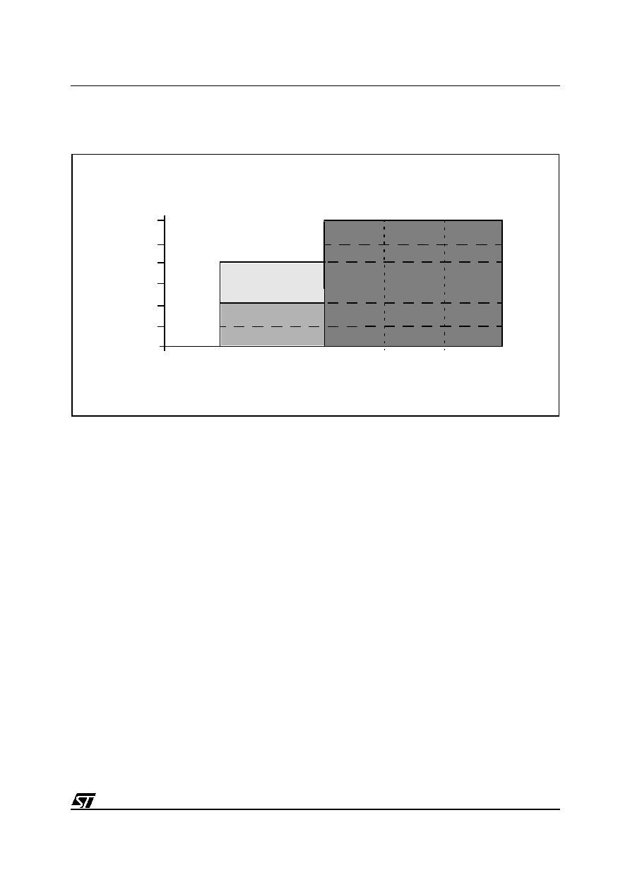
Figure 1, on page 7 shows the operating range of
the ST92163 devices.
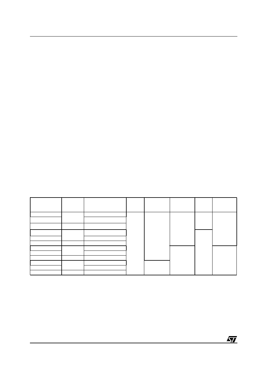
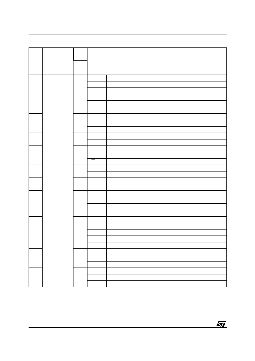
Device Summary
1
Contact sales office for availability
Device
Package
Program Memory
RAM
16-MHz
Low Voltage
Mode
8-MHz
Low Voltage
Mode
LVD
USB
ST92163
1
TQFP64
20K ROM
2K
No
No
Yes
Yes
ST92T163
20K OTP
ST92E163
CQFP64
20K EPROM
ST92163E
1
TQFP64
20K ROM
No
ST92T163E
20K OTP
ST92E163E
CQFP64
20K EPROM
ST92163L
1
TQFP64
20K ROM
Yes
In Normal
Mode only
ST92T163L
20K OTP
ST92E163L
CQFP64
20K EPROM
ST92163V
1
TQFP64
20K ROM
Yes
ST92T163V
1
20K OTP
ST92E163V
1
CQFP64
20K EPROM
7/230
ST92163 - GENERAL DESCRIPTION
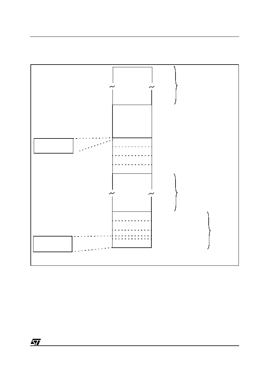
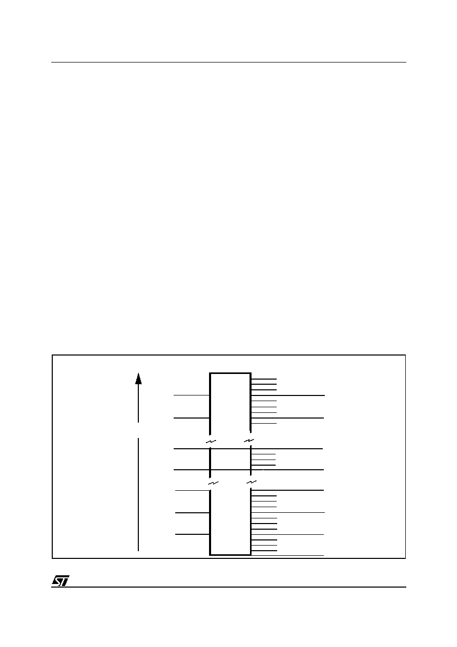
INTRODUCTION (Cont'd)
Figure 1. Maximum Operating Frequency (f
MAX
) versus Supply Voltage (V
DD
)
Notes:
1) This mode is supported by 16-MHz Low Voltage devices only
2) This mode is supported by 8-MHz Low Voltage devices and 16-MHz Low Voltage devices
3) This mode is supported by all devices
0
2.5
4
4.5
5
5.5
24
20
16
12
8
4
MAX FREQUENCY (MHz)
SUPPLY VOLTAGE (V)
3.0
16-MHz LOW VOLTAGE
MODE
1)
FU
N
C
TI
O
N
A
L
I
T
Y
I
S
N
O
T
G
U
AR
AN
T
EED
I
N
T
H
IS
AR
EA
NORMAL VOLTAGE MODE
3)
8-MHz LOW VOLTAGE
MODE
2)
8/230
ST92163 - GENERAL DESCRIPTION
INTRODUCTION (Cont'd)
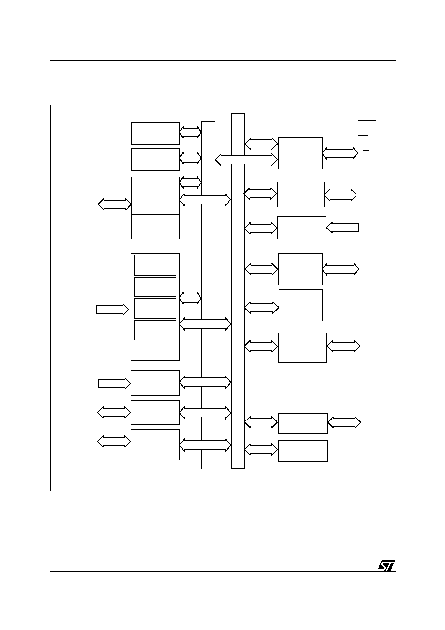
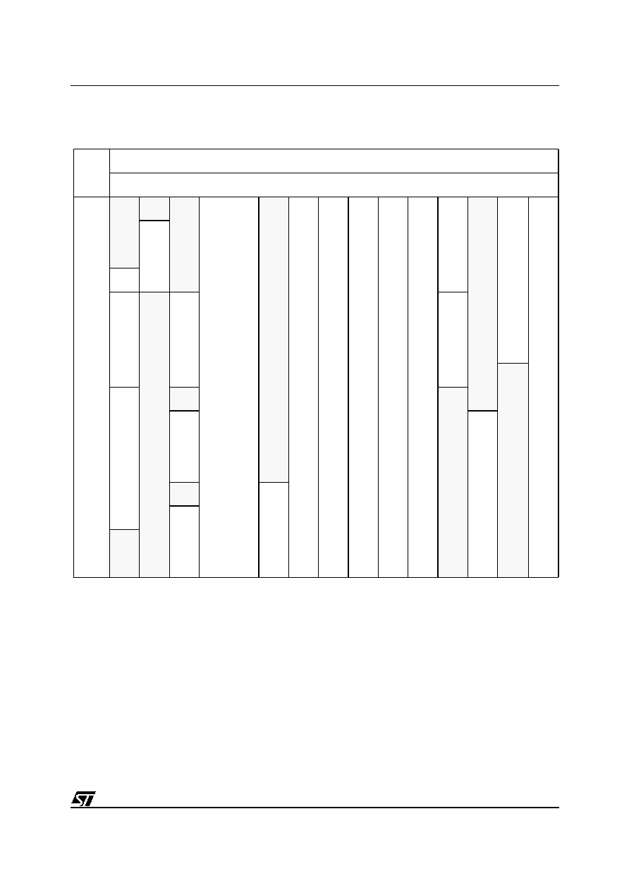
Figure 2. ST92163 Architectural Block Diagram
*64-pin devices only
**on some devices only (refer to "Device Summary" on page 6)
WATCHDOG
TIMER
256 bytes
Register File
2K RAM
ST9+ CORE
8/16-bit
CPU
Interrupt
Management
MEM
ORY BUS
RCCU
External
Memory
Interface
R
EGIS
TER BUS
A/D Converter
AS
BACK
BREQ
DS
WAIT
RW
P0[7:0]
SCI
20K ROM/
EPROM/OTP
AIN[5:0]
EXTRG
TXCLK
RXCLK
SIN
DCD
SOUT
CLKOUT
RTS
SDS
WDIN
WDOUT
All alternate functions (
Italic characters
) are mapped on Ports 0,1, 3, 4, 5 and 6
P3[7:0]
P1[7:0]
SDA
SCL
MF TIMER
USBGND
USBVCC
USBDM0
USBDP0
OSCIN
OSCOUT
RESET
INTCLK
I
2
C BUS
P5[7:0]
Fully Prog.
I/Os
TINA
TINB
TOUTA
TOUTB
INT[7:0]
NMI
P4[3:0]
P6[5:0]
USB
with 16 end-
points
Wakeup
and Interrupt
Management
WKUP[14:0]
P6[7:6]*
A[15:0]
D[7:0]
USBOE
DMA
DMA
5V/3.3V
Voltage
Regulator
Low Voltage
Detector
LVD**
USBSOF
MIRROR
REGISTER

9/230
ST92163 - GENERAL DESCRIPTION
INTRODUCTION (Cont'd)
1.1.1 Core Architecture
The nucleus of the ST92163 is the enhanced ST9
Core that includes the Central Processing Unit
(CPU), the register file, the interrupt and DMA con-
troller, and the Memory Management Unit (MMU).
Three independent buses are controlled by the
Core: a 22-bit memory bus, an 8-bit register ad-
dressing bus and a 6-bit interrupt/DMA bus which
connects the interrupt and DMA controllers in the
on-chip peripherals with the core.
This multiple bus architecture makes the ST9 fam-
ily devices highly efficient for accessing on and
off-chip memory and fast exchange of data with
the on-chip peripherals.
The general-purpose registers can be used as ac-
cumulators, index registers, or address pointers.
Adjacent register pairs make up 16-bit registers for
addressing or 16-bit processing. Although the ST9
has an 8-bit ALU, the chip handles 16-bit opera-
tions, including arithmetic, loads/stores, and mem-
ory/register and memory/memory exchanges.
Many opcodes specify byte or word operations,
the hardware automatically handles 16-bit opera-
tions and accesses.
For interrupts or subroutine calls, the CPU uses a
system stack in conjunction with the stack pointer
(SP). A separate user stack has its own SP. The
separate stacks, without size limitations, can be in
on-chip RAM (or in Register File) or off-chip mem-
ory.
1.1.2 Instruction Set
The ST9 instruction set consists of 94 instruction
types, including instructions for bit handling, byte
(8-bit) and word (16-bit) data, as well as BCD and
Boolean formats. Instructions have been added to
facilitate large program and data handling through
the MMU, as well as to improve the performance
and code density of C Function calls. 14 address-
ing modes are available, including powerful indi-
rect addressing capabilities.
The bit-manipulation instructions of the ST9 are
set, clear, complement, test and set, load, and var-
ious logic instructions (AND, OR, and XOR). Math
functions include add, subtract, increment, decre-
ment, decimal adjust, multiply and divide.
1.1.3 External MEMORY INTERFACE
The ST92163 device has a 16-bit external address
bus allowing it to address up to 64K bytes of exter-
nal memory.
1.1.4 OPERATING MODES
To optimize performance versus the power con-
sumption of the device, ST9 devices now support
a range of operating modes that can be dynami-
cally selected depending on the performance and
functionality requirements of the application at a
given moment.
Run Mode. This is the full speed execution mode
with CPU and peripherals running at the maximum
clock speed delivered by the Phase Locked Loop
(PLL) of the Clock Control Unit (CCU).
Slow Mode. Power consumption can be signifi-
cantly reduced by running the CPU and the periph-
erals at reduced clock speed using the CPU Pres-
caler and CCU Clock Divider.
Wait For Interrupt Mode. The Wait For Interrupt
(WFI) instruction suspends program execution un-
til an interrupt request is acknowledged. During
WFI, the CPU clock is halted while the peripheral
and interrupt controller keep running at a frequen-
cy programmable via the CCU. In this mode, the
power consumption of the device can be reduced
by more than 95% (LP WFI).
Halt Mode. When executing the HALT instruction,
and if the Watchdog is not enabled, the CPU and
its peripherals stop operating and the status of the
machine remains frozen (the clock is also
stopped). A reset is necessary to exit from Halt
mode.
Stop Mode. Under user program control, (see
Wake-up and Interrupt Management Unit), the
CPU and its peripherals stop operating and the
status of the machine remains frozen (the clock is
also stopped) until program execution is woken up
by an event on an external Wake-up pin.

10/230
ST92163 - GENERAL DESCRIPTION
INTRODUCTION (Cont'd)
1.1.5 On-chip Peripherals
USB Interface
The USB interface provides a full speed USB 1.1
compliant port with embedded transceiver and
voltage regulator. Up to 16 endpoints are available
supporting up to 8 USB devices. Separate transmit
and receive DMA channels are available for each
device for fast data transfers with internal RAM.
Parallel I/O Ports
The ST9 is provided with dedicated lines for input/
output. These lines, grouped into 8-bit ports, can
be independently programmed to provide parallel
input/output or to carry input/output signals to or
from the on-chip peripherals and core. All ports
have active pull-ups and pull-down resistors com-
patible with TTL loads. In addition pull-ups can be
turned off for open drain operation and weak pull-
ups can be turned on to save chip resistive pull-
ups. Input buffers can be either TTL or CMOS
compatible.
High Current (10 mA) outputs are available for
driving external devices such as LEDs.
Multifunction Timer
The Multifunction Timer has a 16-bit Up/Down
counter supported by two 16-bit compare regis-
ters, two 16-bit input capture registers and two
DMA channels. Timing resolution can be pro-
grammed using an 8-bit prescaler. 12 operating
modes allow a range of different timing functions
to be easily performed such as complex waveform
generation, measurement or PWM output.
16-bit Timer/Watchdog
The Timer/Watchdog peripheral can be used as a
watchdog or for a wide range of other timing func-
tions such as generating periodic interrupts, meas-
uring input signal pulse widths, requesting an in-
terrupt after a set number of events. It can also
generate a square wave or PWM output signal.
Serial Communications Controller
The SCI provides a synchronous or asynchronous
serial I/O port using two DMA channels. Baud
rates and data formats are programmable. Con-
troller applications can further benefit from the self
test and address wake-up facility offered by the
character search mode.
I
2
C Bus Interface
The I
2
C bus is a synchronous serial bus for con-
necting multiple devices using a data line and a
clock line. Multimaster and slave modes are sup-
ported. Data transfer between the bus and memo-
ry is performed by DMA. The I
2
C interface sup-
ports 7 and 10-bit addressing. It operates in multi-
master or slave mode and supports speeds of up
to 400 KHz. Bus events (Bus busy, slave address
recognized) and error conditions are automatically
flagged in peripheral registers and interrupts are
optionally generated.
Analog/Digital Converter
The ADC provides up to 6 analog inputs with on-
chip sample and hold, fast conversion time and 8-
bit resolution. Conversion can be triggered by a
signal from the Multifunction Timer (MFT).
11/230
ST92163 - GENERAL DESCRIPTION
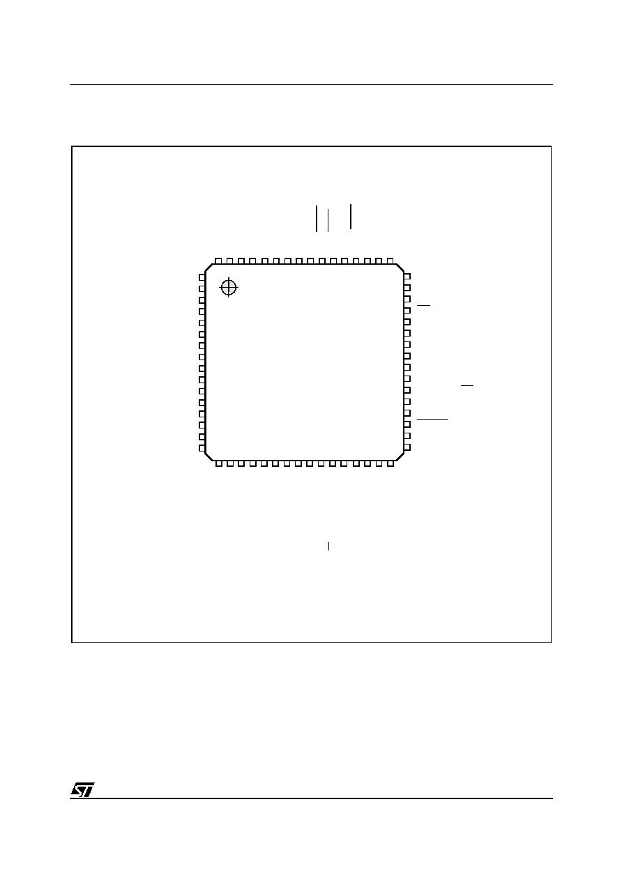
1.2 PIN DESCRIPTION
Figure 3. 64-Pin Package Pin-Out
N.C. = Not connected
WKUP14/A10/P1.2
WKUP14/A9/P1.1
WKUP14/A8/P1.0
D7/A7/P0.7
D6/A6/P0.6
D5/A5/P0.5
D4/A4/P0.4
D3/A3/P0.3
D2/A2/P0.2
D1/A1/P0.1
D0/A0/P0.0
AIN5/P6.7
AIN4/P6.6
USBSOF/AIN3/P6.5
USBSOF/AIN2/P6.4
XTOUT/WKUP13/AIN1/P6.3
P
1.3/A
11/W
KUP
14
P
1.4/A
12/W
KUP
14
P
1.5/A
13/W
KUP
14
P
1.6/A
14/W
KUP
14
P
1.7/A
15/W
KUP
14
N
.C.
N
.C.
V
SS
V
DD
P
4.0/B
REQ
P
4.1/W
AIT
P
4.2
P
4.3//
BACK
U
SBD
M0
U
SBD
P0
N
.C.
N.C.
USBVCC
USBGND
DS
P3.0/INT7/SOUT
P3.1/INT7/RTS
P3.2/INT7/TXCLK/CLKOUT
P3.3/INT7/RXCLK
P3.4/INT7/DCD
P3.5/INT7/SIN
P3.6/INT7/AS
P3.7/INT7/SDS
V
PP
RESET
P5.0/INT1/TINA
N.C.
AV
DD
WKU
P12/
AIN0
/INTC
LK/P6
.2
WK
UP11
/SCL
/EXTR
G/IN
T6/P6
.1
W
KUP
10/S
DA/IN
T5/P6
.0
V
DD
OSC
IN
V
SS
O
SCO
UT
WDO
UT/N
MI/P5
.7
W
KUP9
/TOU
TB/P5
.6
RW
/WD
IN/IN
T0/P5
.5
US
BOE
/WKU
P8/P5
.4
TOU
TA/IN
T2/P5
.3
IN
T3/P5
.2
TI
NB/IN
T4/P5
.1
N
.C.
1
64
16
32
48
16
12/230
ST92163 - GENERAL DESCRIPTION
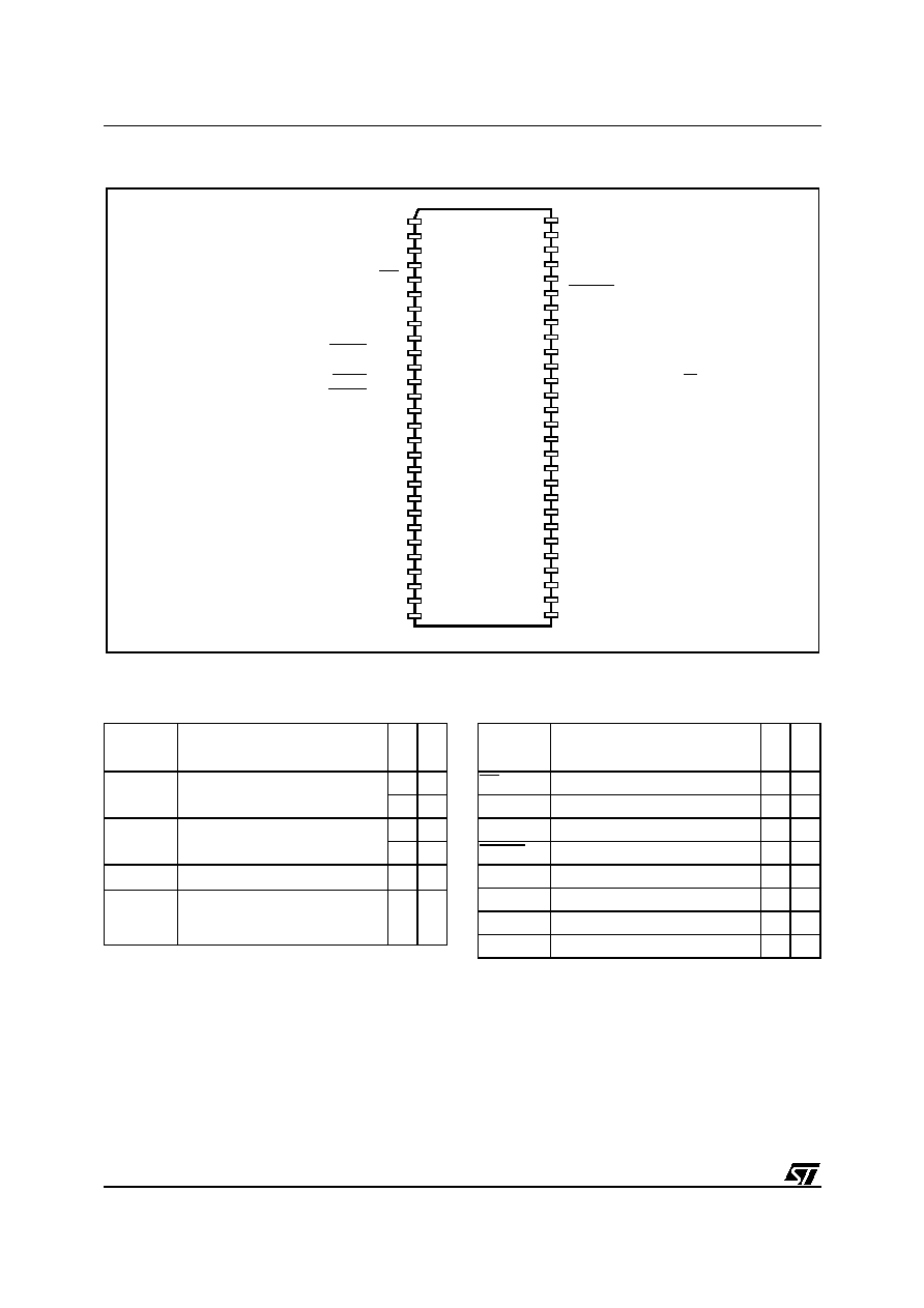
Figure 4. 56-Pin Package Pin-Out
Note: ST92163 devices in DIP56 are available for development purposes.
Table 1. Power Supply Pins
Table 2. Primary Function pins
1
56
29
28
P3.4/INT7/DCD/WKUP4
P3.5/INT7/SIN/WKUP5
P3.6/INT7/ASN/WKUP6
P3.7/INT7/SDS/WKUP7
V
PP
RESET
P5.0/INT1/TINA
P5.1/INT4/TINB
P5.2/INT3
P5.3/INT2/TOUTA
P5.4/WKUP8/USBOE
P5.5/INT0/WDIN/RW
P5.6/TOUTB/WKUP9
P5.7/NMI/WDOUT
OSCOUT
V
SS
OSCIN
V
DD
P6.0/INT5/SDA/WKUP10
P6.1/INT6/EXTRG/SCL/WKUP11
P6.2/INTCLK/AIN0/WKUP12
AV
DD
P6.3/AIN1/WKUP13/XTOUT
P6.4/AIN2/USBSOF
P6.5/AIN3/USBSOF
P0.0/A0/D0
P0.1/A1/D1
P0.2/A2/D2
WKUP3/RXCLK/INT7/P3.3
WKUP2/CLKOUT/TXCLK/INT7/P3.2
WKUP1/RTS/INT7/P3.1
WKUP0/SOUT/INT7/P3.0
DS
USBGND
USBVCC
USBDP0
USBDM0
BACK/P4.3
P4.2
WAIT/P4.1
BREQ/P4.0
V
DD
V
SS
WKUP14/A15/P1.7
WKUP14/A14/P1.6
WKUP14/A13/P1.5
WKUP14/A12/P1.4
WKUP14/A11/P1.3
WKUP14/A10/P1.2
WKUP14/A9/P1.1
WKUP14/A8/P1.0
D7/A7/P0.7
D6/A6/P0.6
D5/A5/P0.5
D4/A4/P0.4
D3/A3/P0.3
Name
Function
D
IP56
Q
FP64
V
DD
Main Power Supply Voltage
(2 pins internally connected)
14
21
39
56
V
SS
Digital Circuit Ground
(2 pins internally connected)
15
23
41
57
AV
DD
Analog Circuit Supply Voltage
35
17
V
PP
EPROM Programming Voltage.
Must be connected to ground in
normal operating mode.
52
36
Name
Function
D
IP56
Q
FP64
DS
Data Strobe
5
45
OSCIN
Oscillator Input
40
22
OSCOUT
Oscillator Output
42
24
RESET
Reset to initialize the ST9
51
35
USBGND
USB bus ground level
6
46
USBVCC
USB voltage regulator output
7
47
USBDM0
USB Upstream port Data- line
9
51
USBDP0
USB Upstream port Data+ line
8
50

13/230
ST92163 - GENERAL DESCRIPTION
1.3 I/O Port Pins
All the ports of the device can be programmed as
Input/Output or in Input mode, compatible with
TTL or CMOS levels (except where Schmitt Trig-
ger is present). Each bit can be programmed indi-
vidually (Refer to the I/O ports chapter).
TTL/CMOS Input
For all those port bits where no input schmitt trig-
ger is implemented, it is always possible to pro-
gram the input level as TTL or CMOS compatible
by programming the relevant PxC2.n control bit.
Refer I/O Ports Chapter to the section titled "Input/
Output Bit Configuration".
Push-Pull/OD Output
The output buffer can be programmed as push-
pull or open-drain: attention must be paid to the
fact that the open-drain option corresponds only to
a disabling of P-channel MOS transistor of the
buffer itself: it is still present and physically con-
nected to the pin. Consequently it is not possible to
increase the output voltage on the pin over
V
DD
+0.3 Volt, to avoid direct junction biasing.
Pure Open-drain Output
The user can increase the voltage on an I/O pin
over V
DD
+0.3 Volt where the P-channel MOS tran-
sistor is physically absent: this is allowed on all
"Pure Open Drain" pins. Of course, in this case the
push-pull option is not available and any weak
pull-up must implemented externally.
Table 3. I/O Port Characteristics
Legend: WPU = Weak Pull-Up, OD = Open Drain
Input
Output
Weak Pull-Up
Reset State
Port 0[7:0]
TTL/CMOS
Push-Pull/OD
Yes
Bidirectional WPU
Port 1[7:0]
TTL/CMOS
Push-Pull/OD
Yes
Bidirectional WPU
Port 3[7:0]
Schmitt trigger
Push-Pull/OD
Yes
Bidirectional WPU
Port 4[3:0]
Schmitt trigger
Push-Pull/OD
Yes
Bidirectional WPU
Port 5[7:0]
Schmitt trigger
Push-Pull/OD
Yes
Bidirectional WPU
Port 6[1:0]
Port 6[5:2]
Port 6.6
Port 6.7
Schmitt trigger
TTL/CMOS
Schmitt trigger
TTL/CMOS
Pure Open Drain with high sink capability
Push-Pull/OD with high sink capability
Push-Pull/OD with high sink capability
Push-Pull/OD with high sink capability
No
Yes
No
No
Bidirectional
Bidirectional WPU
Bidirectional
Bidirectional
14/230
ST92163 - GENERAL DESCRIPTION
Table 4. ST92163 Alternate Functions
Port
Name
General
Purpose I/O
Pin
No.
Alternate Functions
DIP5
6
QFP
64
P0.0
All ports useable
for general pur-
pose I/O (input,
output or bidirec-
tional)
31 11 A0/D0
I/O Ext. Mem. Address/Data bit 0
P0.1
30 10 A1/D1
I/O Ext. Mem. Address/Data bit 1
P0.2
29 9
A2/D2
I/O Ext. Mem. Address/Data bit 2
P0.3
28 8
A3/D3
I/O Ext. Mem. Address/Data bit 3
P0.4
27 7
A4/D4
I/O Ext. Mem. Address/Data bit 4
P0.5
26 6
A5/D5
I/O Ext. Mem. Address/Data bit 5
P0.6
25 5
A6/D6
I/O Ext. Mem. Address/Data bit 6
P0.7
24 4
A7/D7
I/O Ext. Mem. Address/Data bit 7
P1.0
23 3
A8
I/O Ext. Mem. Address bit 8
WKUP14
I
Wakeup Line 14 (***)
P1.1
22 2
A9
I/O Ext. Mem. Address bit 9
WKUP14
I
Wakeup Line 14 (***)
P1.2
21 1
A10
I/O Ext. Mem. Address bit 10
WKUP14
I
Wakeup Line 14 (***)
P1.3
20 64
A11
I/O Ext. Mem. Address bit 11
WKUP14
I
Wakeup Line 14 (***)
P1.4
19 63
A12
I/O Ext. Mem. Address bit 12
WKUP14
I
Wakeup Line 14 (***)
P1.5
18 62
A13
I/O Ext. Mem. Address bit 13
WKUP14
I
Wakeup Line 14 (***)
P1.6
17 61
A14
I/O Ext. Mem. Address bit 14
WKUP14
I
Wakeup Line 14 (***)
P1.7
16 60
A15
I/O Ext. Mem. Address bit 15
WKUP14
I
Wakeup Line 14 (***)
P3.0
4
44
WKUP0
I
Wakeup Line 0
INT7
I
External Interrupt 7 (*)
SOUT
O
SCI Data Output
P3.1
3
43
WKUP1
O
Wakeup Line 1
INT7
I
External Interrupt 7 (*)
RTS
O
SCI Request to Send
15/230
ST92163 - GENERAL DESCRIPTION
P3.2
All ports useable
for general pur-
pose I/O (input,
output or bidirec-
tional)
2
42
WKUP2
I
Wakeup Line 2
INT7
I
External Interrupt 7 (*)
TXCLK
I
SCI Transmit CK Input
CLKOUT
O
SCI Clock Output
P3.3
1
41
WKUP3
I
Wakeup Line 3
INT7
I
External Interrupt 7 (*)
RXCLK
I
SCI Receive CK Input
O
P3.4
56 40
WKUP4
I
Wakeup Line 4
INT7
I
External Interrupt 7 (*)
DCD
I
SCI Data Carrier Detect
O
P3.5
55 39
WKUP5
I
Wakeup Line 5
INT7
I
External Interrupt 7 (*)
SIN
I
SCI Data Input
O
P3.6
54 38
WKUP6
I
Wakeup Line 6
INT7
I
External Interrupt 7 (*)
AS (**)
O
Ext. Mem. Address Strobe
P3.7
53 37
WKUP7
I
Wakeup Line 7
INT7
I
External Interrupt 7 (*)
SDS
O
SCI Synchronous Data Send
P4.0
13 55 BREQ
I
Ext. Mem. Bus Request
P4.1
12 54
WAIT
I
Ext. Mem. Wait Input
RW
O
Ext. Mem. Read/Write Mode Select
P4.2
11 53
I
AS (**)
O
Ext. Mem. Address Strobe
P4.3
10 52
I
BACK
O
Ext. Mem. bus acknow
Port
Name
General
Purpose I/O
Pin
No.
Alternate Functions
D
IP56
Q
FP64
16/230
ST92163 - GENERAL DESCRIPTION
P5.0
All ports useable
for general pur-
pose I/O (input,
output or bidirec-
tional)
50 34
INT1
I
External Interrupt 1
TINA
I
MF Timer Input A
O
P5.1
49 31
INT4
I
External Interrupt 4
TINB
I
MF Timer Input B
O
P5.2
48 30 INT3
I
External Interrupt 3
P5.3
47 29
INT2
I
External Interrupt 2
TOUTA
O
MF Timer Output A
P5.4
46 28
WKUP8
I
Wakeup Line 8
USBOE
O
USB Output enable
P5.5
45 27
WDIN
I
Watchdog Timer Input
INT0
I
External Interrupt 0
RW
O
Ext. Mem. Read/Write Mode Select
P5.6
44 26
WKUP9
I
Wakeup Line 9
TOUTB
O
MF Timer Output B
P5.7
43 25
NMI
I
Non Maskable Interrupt
WDOUT
O
Watchdog Timer Output
P6.0
38 20
WKUP10
I
Wakeup Line 10
INT5
I
External Interrupt 5
SDAI
I
I
2
C Bus Data In
SDAO
O
I
2
C Bus Data Out
P6.1
37 19
WKUP11
I
Wakeup Line 11
INT6
I
External Interrupt 6
SCLI
I
I
2
C Bus Clock In
EXTRG
I
A/D External Trigger
SCLO
O
I
2
C Bus Clock Out
P6.2
36 18
AIN0
I
A/D Analog Input 0
WKUP12
I
Wakeup Line 12
INTCLK
O
Internal Clock
P6.3 34 16
WKUP13
I
Wakeup Line 13
AIN1
I
A/D Analog Input 1
XTOUT
O
Clock Output (same frequency as the external crystal)
Port
Name
General
Purpose I/O
Pin
No.
Alternate Functions
D
IP56
Q
FP64
17/230
ST92163 - GENERAL DESCRIPTION
*Eight interrupt lines internally connected to INT7
through a boolean AND function.
** AS cannot be disabled by software if the ASAF
bit is set (Page Register 245) once the corre-
sponding P3.6 bit is configured as an Alternate
Function output.
***Eight wakeup lines internally connected to
WKUP14 through a boolean AND function.
Note: The reset state of Port 0 and Port 1 is Input,
Weak Pull-Up. To interface external memory, the
ports must be configured by software as alternate
function output.
P6.4
All ports useable
for general pur-
pose I/O (input,
output or bidirec-
tional)
33 15
AIN2
I
A/D Analog Input 2
USBSOF
O
USB SOF Synchro
P6.5
32 14 AIN3
I
A/D Analog Input 3
USBSOF
O
USB SOF Synchro
P6.6
-
13
AIN4
I
A/D Analog Input 4
O
P6.7
-
12
AIN5
I
A/D Analog Input 5
O
Port
Name
General
Purpose I/O
Pin
No.
Alternate Functions
D
IP56
Q
FP64

18/230
ST92163 - GENERAL DESCRIPTION
How to configure the I/O ports
To configure the I/O ports, use the information in
Table 3
and
Table 4
and the Port Bit Configuration
Table in the I/O Ports Chapter on
page 101
.
I/O Note = the hardware characteristics fixed for
each port line.
Inputs:
≠ If I/O note = TTL/CMOS, either TTL or CMOS in-
put level can be selected by software.
≠ If I/O note = Schmitt trigger, selecting CMOS or
TTL input by software has no effect, the input will
always be Schmitt Trigger.
Outputs:
≠ If I/O note = Push-Pull, either Push Pull or Open
Drain can be selected by software.
≠ If I/O note = Open Drain, selecting Push-Pull by
software has no effect, the input will always be
Open Drain.
Alternate Functions (AF) = More than one AF
cannot be assigned to an external pin at the same
time: it can be selected as follows, but simultane-
ous availability of several functions of one pin is
obviously impossible.
AF Inputs:
≠ AF is selected implicitly by enabling the corre-
sponding peripheral. Exceptions to this are ADC
inputs which are selected explicitly as AF by soft-
ware.
AF Outputs or Bidirectional Lines:
≠ In the case of Outputs or I/Os, AF is selected ex-
plicitly by software.
Example 1: Timer/Watchdog input
AF: WDIN, Port: P5.5, I/O note: Input Schmitt Trig-
ger.
Write the port configuration bits:
P5C2.5=1
P5C1.5=0
P5C0.5=1
Enable the WDT peripheral by software as de-
scribed in the WDT chapter.
Example 2: Timer/Watchdog output
AF: WDOUT, Port: P5.7, I/O note: None
Write the port configuration bits:
P5C2.7=0
P5C1.7=1
P5C0.7=1
Example 3: ADC input
AF: AIN0, Port: P6.2, I/O note: Does not apply to
ADC
Write the port configuration bits:
P6C2.2=1
P6C1.2=1
P6C0.2=1
19/230
ST92163 - GENERAL DESCRIPTION
1.4 MEMORY MAP
Figure 5. ST92163 Memory Map
SEGMENT 20h
64 Kbytes
200000h
21FFFFh
20C000h
20BFFFh
208000h
207FFFh
204000h
203FFFh
PAGE 80 - 16 Kbytes
PAGE 81 - 16 Kbytes
PAGE 82 - 16 Kbytes
PAGE 83 - 16 Kbytes
20F800h
20FFFFh
Note: Internal RAM addresses are
RAM
2 Kbytes
Reserved
Internal
External
Memory
Reserved
External
Memory
SEGMENT 21h
64 Kbytes
Internal ROM/EPROM
20FFFFh
220000h
3FFFFFh
repeated each 2 Kbytes inside segment 20h.
Lower Memory
(usually external ROM/EPROM
Upper Memory
(usually external RAM mapped
210000h
Note: The total amount of external memory is 64 Kbytes.
mapped in Segment 1)
in Segment 23h)
1FFFFFh
010000h
00FFFFh
00C000h
00BFFFh
008000h
007FFFh
004000h
000000h
003FFFh
PAGE 0 - 16 Kbytes
PAGE 1 - 16 Kbytes
PAGE 2 - 16 Kbytes
PAGE 3 - 16 Kbytes
64 Kbytes
SEGMENT 0
000000h
004FFFh
ROM/EPROM
20 Kbytes
Internal

20/230
ST92163 - GENERAL DESCRIPTION
1.5 ST92163 REGISTER MAP
Table 6
contains the map of the group F peripheral
pages.
The common registers used by each peripheral
are listed in
Table 5
.
Be very careful to correctly program both:
≠ The set of registers dedicated to a particular
function or peripheral.
≠ Registers common to other functions.
≠ In particular, double-check that any registers
with "undefined" reset values have been correct-
ly initialized.
Warning: Note that in the EIVR and each IVR reg-
ister, all bits are significant. Take care when defin-
ing base vector addresses that entries in the Inter-
rupt Vector table do not overlap.
Table 5. Common Registers
Figure 6. ST92163 Register Groups
Function or Peripheral
Common Registers
SCI, MFT
CICR + NICR + DMA REGISTERS + I/O PORT REGISTERS
ADC
CICR + NICR + I/O PORT REGISTERS
WDT
CICR + NICR + EXTERNAL INTERRUPT REGISTERS +
I/O PORT REGISTERS
I/O PORTS
I/O PORT REGISTERS + MODER
EXTERNAL INTERRUPT
INTERRUPT REGISTERS + I/O PORT REGISTERS
RCCU
INTERRUPT REGISTERS + MODER
REGISTER FILE
SYSTEM REGISTERS
255
240
239
224
223
F
E
D
C
B
A
9
8
7
6
5
4
3
2
1
0
15
0
0
PAGED REGISTERS
These register groups (16 registers per group)
The amount of reserved registers depends on
the number of endpoints used in the program.
(8 registers are used per endpoint).
for USB DMA.
are potentially reserved
21/230
ST92163 - GENERAL DESCRIPTION
Table 6. Group F Pages Register Map
Resources available on the ST92163 device:
Register
Page
0
2
3
4
5
9
10
15
20
21
24
43
55
57
62
R255
Res.
Res.
Res.
USB
Endpoints
Res.
MFT
USB
Com-
mon
I2C
MMU
SCI
Port
9
Res.
WUI
MU
ADC
R254
Port
3
R253
R252
WCR
R251
WDT
Res.
Port
6
Port
8
R250
R249
R248
Res.
R247
EXT
INT
Res.
Res.
R246
Port
5
RCCU
R245
R244
R243
Res.
MFT
R242
Port
4
R241
Res.
R240
22/230
ST92163 - GENERAL DESCRIPTION
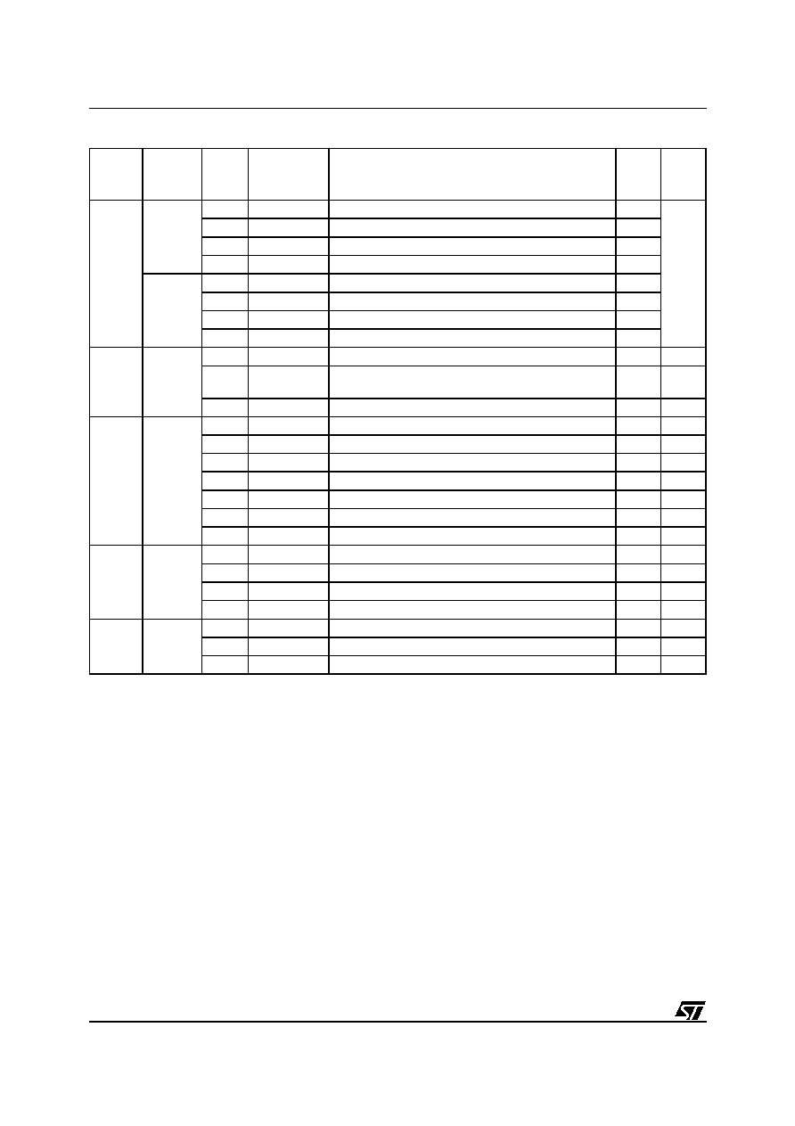
Table 7. Detailed Register Map
Page
No.
Block
Reg.
No.
Register
Name
Description
Reset
Value
Hex.
Doc.
Page
System
I/O
Port
3:5
R227
P3DR
Port 3 Data Register
FF
99
R228
P4DR
Port 4 Data Register
FF
R229
P5DR
Port 5 Data Register
FF
Core
R230
CICR
Central Interrupt Control Register
87
30
R231
FLAGR
Flag Register
00
31
R232
RP0
Pointer 0 Register
00
33
R233
RP1
Pointer 1 Register
00
33
R234
PPR
Page Pointer Register
54
35
R235
MODER
Mode Register
E0
35
R236
USPHR
User Stack Pointer High Register
xx
37
R237
USPLR
User Stack Pointer Low Register
xx
37
R238
SSPHR
System Stack Pointer High Reg.
xx
37
R239
SSPLR
System Stack Pointer Low Reg.
xx
37
0
INT
R242
EITR
External Interrupt Trigger Register
00
59
R243
EIPR
External Interrupt Pending Reg.
00
60
R244
EIMR
External Interrupt Mask-bit Reg.
00
60
R245
EIPLR
External Interrupt Priority Level Reg.
FF
60
R246
EIVR
External Interrupt Vector Register
x6
61
R247
NICR
Nested Interrupt Control
00
61
WDT
R248
WDTHR
Watchdog Timer High Register
FF
110
R249
WDTLR
Watchdog Timer Low Register
FF
110
R250
WDTPR
Watchdog Timer Prescaler Reg.
FF
110
R251
WDTCR
Watchdog Timer Control Register
12
110
R252
WCR
Wait Control Register
7F
111
2
I/O
Port
3
R252
P3C0
Port 3 Configuration Register 0
00
99
R253
P3C1
Port 3 Configuration Register 1
00
R254
P3C2
Port 3 Configuration Register 2
00
3
I/O
Port
4
R240
P4C0
Port 4 Configuration Register 0
00
99
R241
P4C1
Port 4 Configuration Register 1
00
R242
P4C2
Port 4 Configuration Register 2
00
I/O
Port
5
R244
P5C0
Port 5 Configuration Register 0
00
R245
P5C1
Port 5 Configuration Register 1
00
R246
P5C2
Port 5 Configuration Register 2
00
I/O
Port
6
R248
P6C0
Port 6 Configuration Register 0
00
R249
P6C1
Port 6 Configuration Register 1
00
R250
P6C2
Port 6 Configuration Register 2
00
R251
P6DR
Port 6 Data Register
FF
23/230
ST92163 - GENERAL DESCRIPTION
4
USB
End
Points
R240
EP0RA
Endpoint 0 Register A (Transmission)
00
151
R241
EP0RB
Endpoint 0 Register B (Reception)
00
R242
EP1RA
Endpoint 1 Register A (Transmission)
00
R243
EP1RB
Endpoint 1 Register B (Reception)
00
R244
EP2RA
Endpoint 2 Register A (Transmission)
00
R245
EP2RB
Endpoint 2 Register B (Reception)
00
R246
EP3RA
Endpoint 3 Register A (Transmission)
00
R247
EP3RB
Endpoint 3 Register B (Reception)
00
R248
EP4RA
Endpoint 4 Register A (Transmission)
00
R249
EP4RB
Endpoint 4 Register B (Reception)
00
R250
EP5RA
Endpoint 5 Register A (Transmission)
00
R251
EP5RB
Endpoint 5 Register B (Reception)
00
R252
EP6RA
Endpoint 6 Register A (Transmission)
00
R253
EP6RB
Endpoint 6 Register B (Reception)
00
R254
EP7RA
Endpoint 7 Register A (Transmission)
00
R255
EP7RB
Endpoint 7 Register B (Reception)
00
5
R240
EP8RA
Endpoint 8 Register A (Transmission)
00
R241
EP8RB
Endpoint 8 Register B (Reception)
00
R242
EP9RA
Endpoint 9 Register A (Transmission)
00
R243
EP9RB
Endpoint 9 Register B (Reception)
00
R244
EP10RA
Endpoint 10 Register A (Transmission)
00
R245
EP10RB
Endpoint 10 Register B (Reception)
00
R246
EP11RA
Endpoint 11 Register A (Transmission)
00
R247
EP11RB
Endpoint 11 Register B (Reception)
00
R248
EP12RA
Endpoint 12 Register A (Transmission)
00
R249
EP12RB
Endpoint 12 Register B (Reception)
00
R250
EP13RA
Endpoint 13 Register A (Transmission)
00
R251
EP13RB
Endpoint 13 Register B (Reception)
00
R252
EP14RA
Endpoint 14 Register A (Transmission)
00
R253
EP14RB
Endpoint 14 Register B (Reception)
00
R254
EP15RA
Endpoint 15 Register A (Transmission)
00
R255
EP15RB
Endpoint 15 Register B (Reception)
00
9
MFT
R240
DCPR
DMA Counter Pointer Register
xx
133
R241
DAPR
DMA Address Pointer Register
xx
134
R242
T_IVR
Interrupt Vector Register
xx
134
R243
IDCR
Interrupt/DMA Control Register
C7
135
R248
IOCR
I/O Connection Register
FC
135
Page
No.
Block
Reg.
No.
Register
Name
Description
Reset
Value
Hex.
Doc.
Page
24/230
ST92163 - GENERAL DESCRIPTION
10
MFT
R240
REG0HR
Capture Load Register 0 High
xx
126
R241
REG0LR
Capture Load Register 0 Low
xx
126
R242
REG1HR
Capture Load Register 1 High
xx
126
R243
REG1LR
Capture Load Register 1 Low
xx
126
R244
CMP0HR
Compare 0 Register High
00
126
R245
CMP0LR
Compare 0 Register Low
00
126
R246
CMP1HR
Compare 1 Register High
00
126
R247
CMP1LR
Compare 1 Register Low
00
126
R248
TCR
Timer Control Register
0x
127
R249
TMR
Timer Mode Register
00
128
R250
T_ICR
External Input Control Register
0x
129
R251
PRSR
Prescaler Register
00
129
R252
OACR
Output A Control Register
xx
130
R253
OBCR
Output B Control Register
xx
131
R254
T_FLAGR
Flags Register
00
31
R255
IDMR
Interrupt/DMA Mask Register
00
133
15
USB
Common
R240
DADDR0
Device Address Register 0
00
146
R241
DADDR1
Device Address Register 1
00
R242
DADDR2
Device Address Register 2
00
R243
DADDR3
Device Address Register 3
00
R244
DADDR4
Device Address Register 4
00
R245
DADDR5
Device Address Register 5
00
R246
DADDR6
Device Address Register 6
00
R247
DADDR7
Device Address Register 7
00
R248
USBIVR
USB Interrupt Vector Register
xx
142
R249
USBISTR
USB Interrupt Status Register
00
142
R250
USBIMR
USB Interrupt Mask Register
00
143
R251
USBIPR
USB Interrupt Priority Register
xx
143
R252
USBCTLR
USB Control Register
17
144
R253
CTRINF
CTR Interrrupt Flags
xx
145
R254
FNRH
Frame Number Register High
0x
145
R255
FNRL
Frame Number Register Low
xx
145
Page
No.
Block
Reg.
No.
Register
Name
Description
Reset
Value
Hex.
Doc.
Page
25/230
ST92163 - GENERAL DESCRIPTION
20
I2C
R240
I2CCR
I
2
C Control Register
00
189
R241
I2CSR1
I
2
C Status Register 1
00
190
R242
I2CSR2
I
2
C Status Register 2
00
192
R243
I2CCCR
I
2
C Clock Control Register
00
193
R244
I2COAR1
I
2
C Own Address Register 1
00
193
R245
I2COAR2
I
2
C Own Address Register 2
00
194
R246
I2CDR
I
2
C Data Register
00
194
R247
I2CADR
I
2
C General Call Address
A0
194
R248
I2CISR
I
2
C Interrupt Status Register
xx
195
R249
I2CIVR
I
2
C Interrupt Vector Register
xx
196
R250
I2CRDAP
Receiver DMA Source Addr. Pointer
xx
196
R251
I2CRDC
Receiver DMA Transaction Counter
xx
196
R252
I2CTDAP
Transmitter DMA Source Addr. Pointer
xx
197
R253
I2CTDC
Transmitter DMA Transaction Counter
xx
197
R254
I2CECCR
I
2
C Extended Clock Control Register
00
197
R255
I2CIMR
I
2
C Interrupt Mask Register
x0
198
21
MMU
R240
DPR0
Data Page Register 0
00
42
R241
DPR1
Data Page Register 1
01
42
R242
DPR2
Data Page Register 2
02
42
R243
DPR3
Data Page Register 3
83
42
R244
CSR
Code Segment Register
00
43
R248
ISR
Interrupt Segment Register
x0
43
R249
DMASR
DMA Segment Register
x0
43
EXTMI
R245
EMR1
External Memory Register 1
80
96
R246
EMR2
External Memory Register 2
0F
97
24
SCI
R240
RDCPR
Receiver DMA Transaction Counter Pointer
xx
168
R241
RDAPR
Receiver DMA Source Address Pointer
xx
168
R242
TDCPR
Transmitter DMA Transaction Counter Pointer
xx
168
R243
TDAPR
Transmitter DMA Destination Address Pointer
xx
168
R244
S_IVR
Interrupt Vector Register
xx
169
R245
ACR
Address/Data Compare Register
xx
169
R246
IMR
Interrupt Mask Register
x0
170
R247
S_ISR
Interrupt Status Register
xx
43
R248
RXBR
Receive Buffer Register
xx
172
R248
TXBR
Transmitter Buffer Register
xx
172
R249
IDPR
Interrupt/DMA Priority Register
xx
173
R250
CHCR
Character Configuration Register
xx
174
R251
CCR
Clock Configuration Register
00
175
R252
BRGHR
Baud Rate Generator High Reg.
xx
176
R253
BRGLR
Baud Rate Generator Low Register
xx
176
R254
SICR
Synchronous Input Control
03
176
R255
SOCR
Synchronous Output Control
01
177
Page
No.
Block
Reg.
No.
Register
Name
Description
Reset
Value
Hex.
Doc.
Page
26/230
ST92163 - GENERAL DESCRIPTION
Note: xx denotes a byte with an undefined value, but some bits may have defined values. See register description for de-
tails.
43
I/O
Port
8
R248
P8C0
Port 8 Configuration Register 0
00
99
R249
P8C1
Port 8 Configuration Register 1
00
R250
P8C2
Port 8 Configuration Register 2
00
R251
P8DR
Port 8 Data Register
FF
I/O
Port
9
R252
P9C0
Port 9 Configuration Register 0
00
R253
P9C1
Port 9 Configuration Register 1
00
R254
P9C2
Port 9 Configuration Register 2
00
R255
P9DR
Port 9 Data Register
FF
55
RCCU
R240
CLKCTL
Clock Control Register
00
81
R242
CLK_FLAG
Clock Flag Register
48, 28
or 08
82
R246
PLLCONF
PLL Configuration Register
xx
83
59
WUIMU
R249
WUCTRL
Wake-Up Control Register
00
67
R250
WUMRH
Wake-Up Mask Register High
00
68
R251
WUMRL
Wake-Up Mask Register Low
00
68
R252
WUTRH
Wake-Up Trigger Register High
00
69
R253
WUTRL
Wake-Up Trigger Register Low
00
69
R254
WUPRH
Wake-Up Pending Register High
00
69
R255
WUPRL
Wake-Up Pending Register Low
00
69
60
USB
R244
DEVCONF1
USB device configuration 1
0F
149
R245
DEVCONF2
USB device configuration 2
00
149
R246
MIRRA
Mirror Register A
xx
150
R247
MIRRB
Mirror Register B
xx
150
62
ADC
R240
ADDTR
Channel i Data Register
xx
202
R241
ADCLR
Control Logic Register
00
202
R242
ADINT
AD Interrupt Register
01
203
Page
No.
Block
Reg.
No.
Register
Name
Description
Reset
Value
Hex.
Doc.
Page
27/230
ST92163 - DEVICE ARCHITECTURE
2 DEVICE ARCHITECTURE
2.1 CORE ARCHITECTURE
The ST9 Core or Central Processing Unit (CPU)
features a highly optimised instruction set, capable
of handling bit, byte (8-bit) and word (16-bit) data,
as well as BCD and Boolean formats; 14 address-
ing modes are available.
Four independent buses are controlled by the
Core: a 16-bit Memory bus, an 8-bit Register data
bus, an 8-bit Register address bus and a 6-bit In-
terrupt/DMA bus which connects the interrupt and
DMA controllers in the on-chip peripherals with the
Core.
This multiple bus architecture affords a high de-
gree of pipelining and parallel operation, thus mak-
ing the ST9 family devices highly efficient, both for
numerical calculation, data handling and with re-
gard to communication with on-chip peripheral re-
sources.
2.2 MEMORY SPACES
There are two separate memory spaces:
≠ The Register File, which comprises 240 8-bit
registers, arranged as 15 groups (Group 0 to E),
each containing sixteen 8-bit registers plus up to
64 pages of 16 registers mapped in Group F,
which hold data and control bits for the on-chip
peripherals and I/Os.
≠ A single linear memory space accommodating
both program and data. All of the physically sep-
arate memory areas, including the internal ROM,
internal RAM and external memory are mapped
in this common address space. The total ad-
dressable memory space of 4 Mbytes (limited by
the size of on-chip memory and the number of
external address pins) is arranged as 64 seg-
ments of 64 Kbytes. Each segment is further
subdivided into four pages of 16 Kbytes, as illus-
trated in
Figure 1
. A Memory Management Unit
uses a set of pointer registers to address a 22-bit
memory field using 16-bit address-based instruc-
tions.
2.2.1 Register File
The Register File consists of (see
Figure 2
):
≠ 224 general purpose registers (Group 0 to D,
registers R0 to R223)
≠ 6 system registers in the System Group (Group
E, registers R224 to R239)
≠ Up to 64 pages, depending on device configura-
tion, each containing up to 16 registers, mapped
to Group F (R240 to R255), see
Figure 3
.
Figure 7. Single Program and Data Memory Address Space
3FFFFFh
3F0000h
3EFFFFh
3E0000h
20FFFFh
02FFFFh
020000h
01FFFFh
010000h
00FFFFh
000000h
8
7
6
5
4
3
2
1
0
63
62
2
1
0
Address
16K Pages
64K Segments
up to 4 Mbytes
Data
Code
255
254
253
252
251
250
249
248
247
9
10
11
21FFFFh
210000h
133
134
135
33
Reserved
132
28/230
ST92163 - DEVICE ARCHITECTURE
MEMORY SPACES (Cont'd)
Figure 8. Register Groups
Figure 9. Page Pointer for Group F mapping
Figure 10. Addressing the Register File
F
E
D
C
B
A
9
8
7
6
5
4
3
PAGED REGISTERS
SYSTEM REGISTERS
2
1
0
0
0
15
255
240
239
224
223
VA00432
UP TO
64 PAGES
GENERAL
REGISTERS
PURPOSE
224
PAGE 63
PAGE 5
PAGE 0
PAGE POINTER
R255
R240
R224
R0
VA00433
R234
REGISTER FILE
SYSTEM REGISTERS
GROUP D
GROUP B
GROUP C
(1100) (0011)
R192
R207
255
240
239
224
223
F
E
D
C
B
A
9
8
7
6
5
4
3
2
1
0
15
VR000118
0
0
R195
R195
(R0C3h)
PAGED REGISTERS

29/230
ST92163 - DEVICE ARCHITECTURE
MEMORY SPACES (Cont'd)
2.2.2 Register Addressing
Register File registers, including Group F paged
registers (but excluding Group D), may be ad-
dressed explicitly by means of a decimal, hexa-
decimal or binary address; thus
R231, RE7h
and
R11100111b
represent the same register (see
Figure 4
). Group D registers can only be ad-
dressed in Working Register mode.
Note that an upper case "
R
" is used to denote this
direct addressing mode.
Working Registers
Certain types of instruction require that registers
be specified in the form "
rx
", where
x
is in the
range 0 to 15: these are known as Working Regis-
ters.
Note that a lower case "
r
" is used to denote this in-
direct addressing mode.
Two addressing schemes are available: a single
group of 16 working registers, or two separately
mapped groups, each consisting of 8 working reg-
isters. These groups may be mapped starting at
any 8 or 16 byte boundary in the register file by
means of dedicated pointer registers. This tech-
nique is described in more detail in
Section 1.3.3
,
and illustrated in
Figure 5
and in
Figure 6
.
System Registers
The 16 registers in Group E (R224 to R239) are
System registers and may be addressed using any
of the register addressing modes. These registers
are described in greater detail in
Section 1.3
.
Paged Registers
Up to 64 pages, each containing 16 registers, may
be mapped to Group F. These are addressed us-
ing any register addressing mode, in conjunction
with the Page Pointer register, R234, which is one
of the System registers. This register selects the
page to be mapped to Group F and, once set,
does not need to be changed if two or more regis-
ters on the same page are to be addressed in suc-
cession.
Therefore if the Page Pointer, R234, is set to 5, the
instructions:
spp #5
ld R242, r4
will load the contents of working register r4 into the
third register of page 5 (R242).
These paged registers hold data and control infor-
mation relating to the on-chip peripherals, each
peripheral always being associated with the same
pages and registers to ensure code compatibility
between ST9 devices. The number of these regis-
ters therefore depends on the peripherals which
are present in the specific ST9 family device. In
other words, pages only exist if the relevant pe-
ripheral is present.
Table 8. Register File Organization
Hex.
Address
Decimal
Address
Function
Register
File Group
F0-FF
240-255
Paged
Registers
Group F
E0-EF
224-239
System
Registers
Group E
D0-DF
208-223
General
Purpose
Registers
Group D
C0-CF
192-207
Group C
B0-BF
176-191
Group B
A0-AF
160-175
Group A
90-9F
144-159
Group 9
80-8F
128-143
Group 8
70-7F
112-127
Group 7
60-6F
96-111
Group 6
50-5F
80-95
Group 5
40-4F
64-79
Group 4
30-3F
48-63
Group 3
20-2F
32-47
Group 2
10-1F
16-31
Group 1
00-0F
00-15
Group 0

30/230
ST92163 - DEVICE ARCHITECTURE
2.3 SYSTEM REGISTERS
The System registers are listed in
Table 2 System
Registers (Group E)
. They are used to perform all
the important system settings. Their purpose is de-
scribed in the following pages. Refer to the chapter
dealing with I/O for a description of the PORT[5:0]
Data registers.
Table 9. System Registers (Group E)
2.3.1 Central Interrupt Control Register
Please refer to the "INTERRUPT" chapter for a de-
tailed description of the ST9 interrupt philosophy.
CENTRAL INTERRUPT CONTROL REGISTER
(CICR)
R230 - Read/Write
Register Group: E (System)
Reset Value: 1000 0111 (87h)
Bit 7 = GCEN:
Global Counter Enable
.
This bit is the Global Counter Enable of the Multi-
function Timers. The GCEN bit is ANDed with the
CE bit in the TCR Register (only in devices featur-
ing the MFT Multifunction Timer) in order to enable
the Timers when both bits are set. This bit is set af-
ter the Reset cycle.
Note: If an MFT is not included in the ST9 device,
then this bit has no effect.
Bit 6 = TLIP:
Top Level Interrupt
Pending
.
This bit is set by hardware when a Top Level Inter-
rupt Request is recognized. This bit can also be
set by software to simulate a Top Level Interrupt
Request.
0: No Top Level Interrupt pending
1: Top Level Interrupt pending
Bit 5 = TLI:
Top Level Interrupt bit
.
0: Top Level Interrupt is acknowledged depending
on the TLNM bit in the NICR Register.
1: Top Level Interrupt is acknowledged depending
on the IEN and TLNM bits in the NICR Register
(described in the Interrupt chapter).
Bit 4 = IEN:
Interrupt Enable .
This bit is cleared by interrupt acknowledgement,
and set by interrupt return (
iret
). IEN is modified
implicitly by
iret
,
ei
and
di
instructions or by an
interrupt acknowledge cycle. It can also be explic-
itly written by the user, but only when no interrupt
is pending. Therefore, the user should execute a
di
instruction (or guarantee by other means that
no interrupt request can arrive) before any write
operation to the CICR register.
0: Disable all interrupts except Top Level Interrupt.
1: Enable Interrupts
Bit 3 = IAM:
Interrupt Arbitration Mode
.
This bit is set and cleared by software to select the
arbitration mode.
0: Concurrent Mode
1: Nested Mode.
Bits 2:0 = CPL[2:0]:
Current Priority Level
.
These three bits record the priority level of the rou-
tine currently running (i.e. the Current Priority Lev-
el, CPL). The highest priority level is represented
by 000, and the lowest by 111. The CPL bits can
be set by hardware or software and provide the
reference according to which subsequent inter-
rupts are either left pending or are allowed to inter-
rupt the current interrupt service routine. When the
current interrupt is replaced by one of a higher pri-
ority, the current priority value is automatically
stored until required in the NICR register.
R239 (EFh)
SSPLR
R238 (EEh)
SSPHR
R237 (EDh)
USPLR
R236 (ECh)
USPHR
R235 (EBh)
MODE REGISTER
R234 (EAh)
PAGE POINTER REGISTER
R233 (E9h)
REGISTER POINTER 1
R232 (E8h)
REGISTER POINTER 0
R231 (E7h)
FLAG REGISTER
R230 (E6h)
CENTRAL INT. CNTL REG
R229 (E5h)
PORT5 DATA REG.
R228 (E4h)
PORT4 DATA REG.
R227 (E3h)
PORT3 DATA REG.
R226 (E2h)
PORT2 DATA REG.
R225 (E1h)
PORT1 DATA REG.
R224 (E0h)
PORT0 DATA REG.
7
0
GCEN
TLIP
TLI
IEN
IAM
CPL2 CPL1 CPL0

31/230
ST92163 - DEVICE ARCHITECTURE
SYSTEM REGISTERS (Cont'd)
2.3.2 Flag Register
The Flag Register contains 8 flags which indicate
the CPU status. During an interrupt, the flag regis-
ter is automatically stored in the system stack area
and recalled at the end of the interrupt service rou-
tine, thus returning the CPU to its original status.
This occurs for all interrupts and, when operating
in nested mode, up to seven versions of the flag
register may be stored.
FLAG REGISTER (FLAGR)
R231- Read/Write
Register Group: E (System)
Reset value: 0000 0000 (00h)
Bit 7 = C:
Carry Flag
.
The carry flag is affected by:
Addition (
add, addw, adc, adcw
),
Subtraction (
sub, subw, sbc, sbcw
),
Compare (
cp, cpw
),
Shift Right Arithmetic (
sra, sraw
),
Shift Left Arithmetic (
sla, slaw
),
Swap Nibbles (
swap
),
Rotate (
rrc, rrcw, rlc, rlcw, ror,
rol
),
Decimal Adjust (
da
),
Multiply and Divide (
mul, div, divws
).
When set, it generally indicates a carry out of the
most significant bit position of the register being
used as an accumulator (bit 7 for byte operations
and bit 15 for word operations).
The carry flag can be set by the Set Carry Flag
(
scf
) instruction, cleared by the Reset Carry Flag
(
rcf
) instruction, and complemented by the Com-
plement Carry Flag (
ccf
) instruction.
Bit 6 = Z:
Zero Flag
. The Zero flag is affected by:
Addition (
add, addw, adc, adcw
),
Subtraction (
sub, subw, sbc, sbcw
),
Compare (
cp, cpw
),
Shift Right Arithmetic (
sra, sraw
),
Shift Left Arithmetic (
sla, slaw
),
Swap Nibbles (
swap
),
Rotate (rrc
, rrcw, rlc, rlcw, ror,
rol)
,
Decimal Adjust (
da
),
Multiply and Divide (
mul, div, divws
),
Logical (
and, andw, or, orw, xor,
xorw, cpl
),
Increment and Decrement (
inc, incw, dec,
decw
),
Test (
tm, tmw, tcm, tcmw, btset
).
In most cases, the Zero flag is set when the contents
of the register being used as an accumulator be-
come zero, following one of the above operations.
Bit 5 = S:
Sign Flag
.
The Sign flag is affected by the same instructions
as the Zero flag.
The Sign flag is set when bit 7 (for a byte opera-
tion) or bit 15 (for a word operation) of the register
used as an accumulator is one.
Bit 4 = V:
Overflow Flag
.
The Overflow flag is affected by the same instruc-
tions as the Zero and Sign flags.
When set, the Overflow flag indicates that a two's-
complement number, in a result register, is in er-
ror, since it has exceeded the largest (or is less
than the smallest), number that can be represent-
ed in two's-complement notation.
Bit 3 = DA:
Decimal Adjust Flag
.
The DA flag is used for BCD arithmetic. Since the
algorithm for correcting BCD operations is differ-
ent for addition and subtraction, this flag is used to
specify which type of instruction was executed
last, so that the subsequent Decimal Adjust (
da
)
operation can perform its function correctly. The
DA flag cannot normally be used as a test condi-
tion by the programmer.
Bit 2 = H:
Half Carry Flag.
The H flag indicates a carry out of (or a borrow in-
to) bit 3, as the result of adding or subtracting two
8-bit bytes, each representing two BCD digits. The
H flag is used by the Decimal Adjust (
da
) instruc-
tion to convert the binary result of a previous addi-
tion or subtraction into the correct BCD result. Like
the DA flag, this flag is not normally accessed by
the user.
Bit 1 = Reserved bit (must be 0).
Bit 0 = DP:
Data/Program Memory Flag
.
This bit indicates the memory area addressed. Its
value is affected by the Set Data Memory (
sdm
)
and Set Program Memory (
spm
) instructions. Re-
fer to the Memory Management Unit for further de-
tails.
7
0
C
Z
S
V
DA
H
-
DP

32/230
ST92163 - DEVICE ARCHITECTURE
SYSTEM REGISTERS (Cont'd)
If the bit is set, data is accessed using the Data
Pointers (DPRs registers), otherwise it is pointed
to by the Code Pointer (CSR register); therefore,
the user initialization routine must include a
Sdm
instruction. Note that code is always pointed to by
the Code Pointer (CSR).
Note: In the current ST9 devices, the DP flag is
only for compatibility with software developed for
the first generation of ST9 devices. With the single
memory addressing space, its use is now redun-
dant. It must be kept to 1 with a
Sdm
instruction at
the beginning of the program to ensure a normal
use of the different memory pointers.
2.3.3 Register Pointing Techniques
Two registers within the System register group,
are used as pointers to the working registers. Reg-
ister Pointer 0 (R232) may be used on its own as a
single pointer to a 16-register working space, or in
conjunction with Register Pointer 1 (R233), to
point to two separate 8-register spaces.
For the purpose of register pointing, the 16 register
groups of the register file are subdivided into 32 8-
register blocks. The values specified with the Set
Register Pointer instructions refer to the blocks to
be pointed to in twin 8-register mode, or to the low-
er 8-register block location in single 16-register
mode.
The Set Register Pointer instructions
srp
,
srp0
and
srp1
automatically inform the CPU whether
the Register File is to operate in single 16-register
mode or in twin 8-register mode. The
srp
instruc-
tion selects the single 16-register group mode and
specifies the location of the lower 8-register block,
while the
srp0
and
srp1
instructions automatical-
ly select the twin 8-register group mode and spec-
ify the locations of each 8-register block.
There is no limitation on the order or position of
these register groups, other than that they must
start on an 8-register boundary in twin 8-register
mode, or on a 16-register boundary in single 16-
register mode.
The block number should always be an even
number in single 16-register mode. The 16-regis-
ter group will always start at the block whose
number is the nearest even number equal to or
lower than the block number specified in the
srp
instruction. Avoid using odd block numbers, since
this can be confusing if twin mode is subsequently
selected.
Thus:
srp #3
will be interpreted as
srp #2
and will al-
low using R16 ..R31 as r0 .. r15.
In single 16-register mode, the working registers
are referred to as
r0
to
r15
. In twin 8-register
mode, registers
r0
to
r7
are in the block pointed
to by RP0 (by means of the
srp0
instruction),
while registers
r8
to
r15
are in the block pointed
to by RP1 (by means of the
srp1
instruction).
Caution:
Group D registers can only be accessed
as working registers using the Register Pointers,
or by means of the Stack Pointers. They cannot be
addressed explicitly in the form "
Rxxx
".

33/230
ST92163 - DEVICE ARCHITECTURE
SYSTEM REGISTERS (Cont'd)
POINTER 0 REGISTER (RP0)
R232 - Read/Write
Register Group: E (System)
Reset Value: xxxx xx00 (xxh)
Bits 7:3 = RG[4:0]:
Register Group number.
These bits contain the number (in the range 0 to
31) of the register block specified in the
srp0
or
srp
instructions. In single 16-register mode the
number indicates the lower of the two 8-register
blocks to which the 16 working registers are to be
mapped, while in twin 8-register mode it indicates
the 8-register block to which
r0
to
r7
are to be
mapped.
Bit 2 = RPS:
Register Pointer Selector
.
This bit is set by the instructions
srp0
and
srp1
to
indicate that the twin register pointing mode is se-
lected. The bit is reset by the
srp
instruction to in-
dicate that the single register pointing mode is se-
lected.
0: Single register pointing mode
1: Twin register pointing mode
Bits 1:0: Reserved. Forced by hardware to zero.
POINTER 1 REGISTER (RP1)
R233 - Read/Write
Register Group: E (System)
Reset Value: xxxx xx00 (xxh)
This register is only used in the twin register point-
ing mode. When using the single register pointing
mode, or when using only one of the twin register
groups, the RP1 register must be considered as
RESERVED and may NOT be used as a general
purpose register.
Bits 7:3 = RG[4:0]:
Register Group number.
These bits contain the number (in the range 0 to
31) of the 8-register block specified in the
srp1
in-
struction, to which
r8
to
r15
are to be mapped.
Bit 2 = RPS:
Register Pointer Selector
.
This bit is set by the
srp0
and
srp1
instructions to
indicate that the twin register pointing mode is se-
lected. The bit is reset by the
srp
instruction to in-
dicate that the single register pointing mode is se-
lected.
0: Single register pointing mode
1: Twin register pointing mode
Bits 1:0: Reserved. Forced by hardware to zero.
7
0
RG4
RG3
RG2
RG1
RG0
RPS
0
0
7
0
RG4
RG3
RG2
RG1
RG0
RPS
0
0
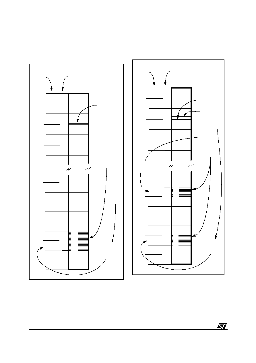
34/230
ST92163 - DEVICE ARCHITECTURE
SYSTEM REGISTERS (Cont'd)
Figure 11. Pointing to a single group of 16
registers
Figure 12. Pointing to two groups of 8 registers
31
30
29
28
27
26
25
9
8
7
6
5
4
3
2
1
0
F
E
D
4
3
2
1
0
BLOCK
NUMBER
REGISTER
GROUP
REGISTER
FILE
REGISTER
POINTER 0
srp #2
set by:
instruction
points to:
GROUP 1
addressed by
BLOCK 2
r15
r0
31
30
29
28
27
26
25
9
8
7
6
5
4
3
2
1
0
F
E
D
4
3
2
1
0
BLOCK
NUMBER
REGISTER
GROUP
REGISTER
FILE
REGISTER
POINTER 0
srp0 #2
set by:
instructions
point to:
GROUP 1
addressed by
BLOCK 2
&
REGISTER
POINTER 1
srp1 #7
&
GROUP 3
addressed by
BLOCK 7
r7
r0
r15
r8
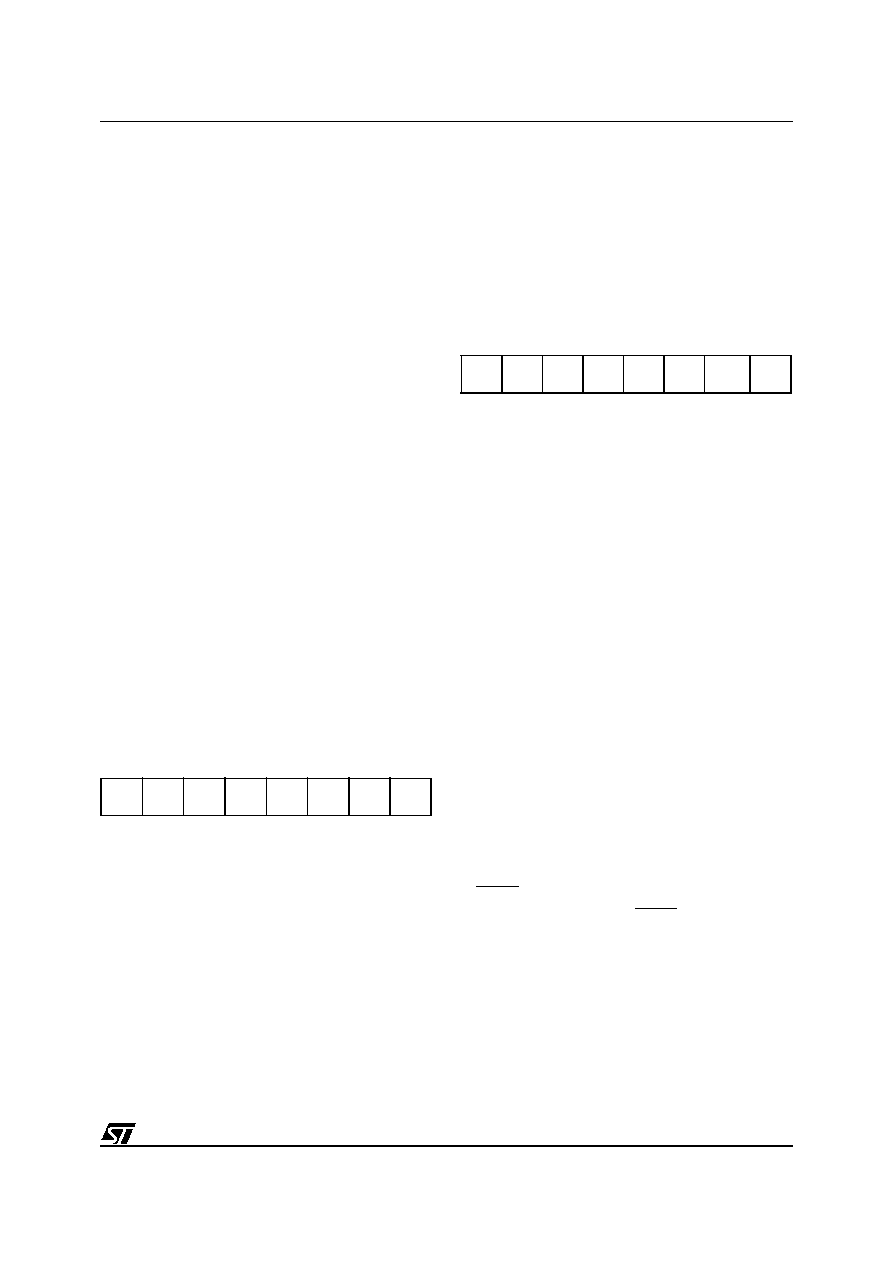
35/230
ST92163 - DEVICE ARCHITECTURE
SYSTEM REGISTERS (Cont'd)
2.3.4 Paged Registers
Up to 64 pages, each containing 16 registers, may
be mapped to Group F. These paged registers
hold data and control information relating to the
on-chip peripherals, each peripheral always being
associated with the same pages and registers to
ensure code compatibility between ST9 devices.
The number of these registers depends on the pe-
ripherals present in the specific ST9 device. In oth-
er words, pages only exist if the relevant peripher-
al is present.
The paged registers are addressed using the nor-
mal register addressing modes, in conjunction with
the Page Pointer register, R234, which is one of
the System registers. This register selects the
page to be mapped to Group F and, once set,
does not need to be changed if two or more regis-
ters on the same page are to be addressed in suc-
cession.
Thus the instructions:
spp #5
ld R242, r4
will load the contents of working register r4 into the
third register of page 5 (R242).
Warning: During an interrupt, the PPR register is
not saved automatically in the stack. If needed, it
should be saved/restored by the user within the in-
terrupt routine.
PAGE POINTER REGISTER (PPR)
R234 - Read/Write
Register Group: E (System)
Reset value: xxxx xx00 (xxh)
Bits 7:2 = PP[5:0]:
Page Pointer
.
These bits contain the number (in the range 0 to
63) of the page specified in the
spp
instruction.
Once the page pointer has been set, there is no
need to refresh it unless a different page is re-
quired.
Bits 1:0: Reserved. Forced by hardware to 0.
2.3.5 Mode Register
The Mode Register allows control of the following
operating parameters:
≠ Selection of internal or external System and User
Stack areas,
≠ Management of the clock frequency,
≠ Enabling of Bus request and Wait signals when
interfacing to external memory.
MODE REGISTER (MODER)
R235 - Read/Write
Register Group: E (System)
Reset value: 1110 0000 (E0h)
Bit 7 = SSP:
System Stack Pointer
.
This bit selects an internal or external System
Stack area.
0: External system stack area, in memory space.
1: Internal system stack area, in the Register File
(reset state).
Bit 6 = USP:
User Stack Pointer
.
This bit selects an internal or external User Stack
area.
0: External user stack area, in memory space.
1: Internal user stack area, in the Register File (re-
set state).
Bit 5 = DIV2:
Crystal Oscillator Clock Divided by 2
.
This bit controls the divide-by-2 circuit operating
on the crystal oscillator clock (CLOCK1).
0: Clock divided by 1
1: Clock divided by 2
Bits 4:2 = PRS[2:0]:
CPUCLK Prescaler
.
These bits load the prescaler division factor for the
internal clock (INTCLK). The prescaler factor se-
lects the internal clock frequency, which can be di-
vided by a factor from 1 to 8. Refer to the Reset
and Clock Control chapter for further information.
Bit 1 = BRQEN:
Bus Request Enable
.
0: External Memory Bus Request disabled
1: External Memory Bus Request enabled on
BREQ pin (where available).
Note: Disregard this bit if BREQ pin is not availa-
ble.
Bit 0 = HIMP:
High Impedance Enable
.
When any of Ports 0, 1, 2 or 6 depending on de-
vice configuration, are programmed as Address
and Data lines to interface external Memory, these
lines and the Memory interface control lines (AS,
DS, R/W) can be forced into the High Impedance
7
0
PP5
PP4
PP3
PP2
PP1
PP0
0
0
7
0
SSP
USP
DIV2
PRS2
PRS1
PRS0 BRQEN HIMP

36/230
ST92163 - DEVICE ARCHITECTURE
SYSTEM REGISTERS (Cont'd)
state by setting the HIMP bit. When this bit is reset,
it has no effect.
Setting the HIMP bit is recommended for noise re-
duction when only internal Memory is used.
If Port 1 and/or 2 are declared as an address AND
as an I/O port (for example: P10... P14 = Address,
and P15... P17 = I/O), the HIMP bit has no effect
on the I/O lines.
2.3.6 Stack Pointers
Two separate, double-register stack pointers are
available: the System Stack Pointer and the User
Stack Pointer, both of which can address registers
or memory.
The stack pointers point to the "bottom" of the
stacks which are filled using the push commands
and emptied using the pop commands. The stack
pointer is automatically pre-decremented when
data is "pushed" in and post-incremented when
data is "popped" out.
The push and pop commands used to manage the
System Stack may be addressed to the User
Stack by adding the suffix "
u"
. To use a stack in-
struction for a word, the suffix "
w"
is added. These
suffixes may be combined.
When bytes (or words) are "popped" out from a
stack, the contents of the stack locations are un-
changed until fresh data is loaded. Thus, when
data is "popped" from a stack area, the stack con-
tents remain unchanged.
Note: Instructions such as:
pushuw RR236
or
pushw RR238,
as well as the corresponding
pop
instructions (where R236 & R237, and R238
& R239 are themselves the user and system stack
pointers respectively), must not be used, since the
pointer values are themselves automatically
changed by the
push
or
pop
instruction, thus cor-
rupting their value.
System Stack
The System Stack is used for the temporary stor-
age of system and/or control data, such as the
Flag register and the Program counter.
The following automatically push data onto the
System Stack:
≠ Interrupts
When entering an interrupt, the PC and the Flag
Register are pushed onto the System Stack. If the
ENCSR bit in the EMR2 register is set, then the
Code Segment Register is also pushed onto the
System Stack.
≠ Subroutine Calls
When a
call
instruction is executed, only the PC
is pushed onto stack, whereas when a
calls
in-
struction (call segment) is executed, both the PC
and the Code Segment Register are pushed onto
the System Stack.
≠ Link Instruction
The
link
or
linku
instructions create a C lan-
guage stack frame of user-defined length in the
System or User Stack.
All of the above conditions are associated with
their counterparts, such as return instructions,
which pop the stored data items off the stack.
User Stack
The User Stack provides a totally user-controlled
stacking area.
The User Stack Pointer consists of two registers,
R236 and R237, which are both used for address-
ing a stack in memory. When stacking in the Reg-
ister File, the User Stack Pointer High Register,
R236, becomes redundant but must be consid-
ered as reserved.
Stack Pointers
Both System and User stacks are pointed to by
double-byte stack pointers. Stacks may be set up
in RAM or in the Register File. Only the lower byte
will be required if the stack is in the Register File.
The upper byte must then be considered as re-
served and must not be used as a general purpose
register.
The stack pointer registers are located in the Sys-
tem Group of the Register File, this is illustrated in
Table 2 System Registers (Group E)
.
Stack Location
Care is necessary when managing stacks as there
is no limit to stack sizes apart from the bottom of
any address space in which the stack is placed.
Consequently programmers are advised to use a
stack pointer value as high as possible, particular-
ly when using the Register File as a stacking area.
Group D is a good location for a stack in the Reg-
ister File, since it is the highest available area. The
stacks may be located anywhere in the first 14
groups of the Register File (internal stacks) or in
RAM (external stacks).
Note. Stacks must not be located in the Paged
Register Group or in the System Register Group.
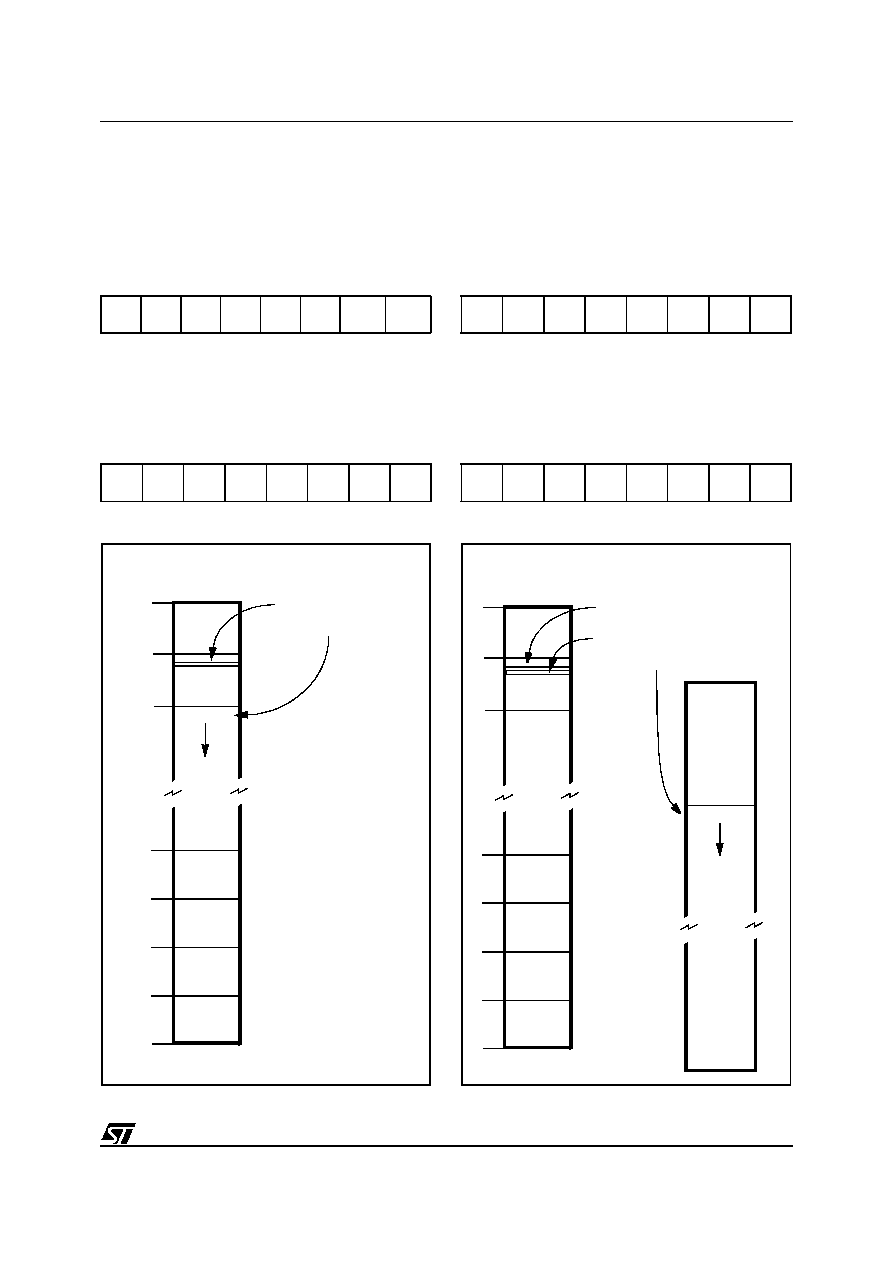
37/230
ST92163 - DEVICE ARCHITECTURE
SYSTEM REGISTERS (Cont'd)
USER STACK POINTER HIGH REGISTER
(USPHR)
R236 - Read/Write
Register Group: E (System)
Reset value: undefined
USER STACK POINTER LOW REGISTER
(USPLR)
R237 - Read/Write
Register Group: E (System)
Reset value: undefined
Figure 13. Internal Stack Mode
SYSTEM STACK POINTER HIGH REGISTER
(SSPHR)
R238 - Read/Write
Register Group: E (System)
Reset value: undefined
SYSTEM STACK POINTER LOW REGISTER
(SSPLR)
R239 - Read/Write
Register Group: E (System)
Reset value: undefined
Figure 14. External Stack Mode
7
0
USP15 USP14 USP13 USP12 USP11 USP10 USP9
USP8
7
0
USP7
USP6
USP5
USP4
USP3
USP2
USP1
USP0
F
E
D
4
3
2
1
0
REGISTER
FILE
STACK POINTER (LOW)
points to:
STACK
7
0
SSP15 SSP14 SSP13 SSP12 SSP11 SSP10 SSP9
SSP8
7
0
SSP7
SSP6
SSP5
SSP4
SSP3
SSP2
SSP1
SSP0
F
E
D
4
3
2
1
0
REGISTER
FILE
STACK POINTER (LOW)
point to:
STACK
MEMORY
STACK POINTER (HIGH)
&

38/230
ST92163 - DEVICE ARCHITECTURE
2.4 MEMORY ORGANIZATION
Code and data are accessed within the same line-
ar address space. All of the physically separate
memory areas, including the internal ROM, inter-
nal RAM and external memory are mapped in a
common address space.
The ST9 provides a total addressable memory
space of 4 Mbytes. This address space is ar-
ranged as 64 segments of 64 Kbytes; each seg-
ment is again subdivided into four 16 Kbyte pages.
The mapping of the various memory areas (inter-
nal RAM or ROM, external memory) differs from
device to device. Each 64-Kbyte physical memory
segment is mapped either internally or externally;
if the memory is internal and smaller than 64
Kbytes, the remaining locations in the 64-Kbyte
segment are not used (reserved).
Refer to the Register and Memory Map Chapter
for more details on the memory map.
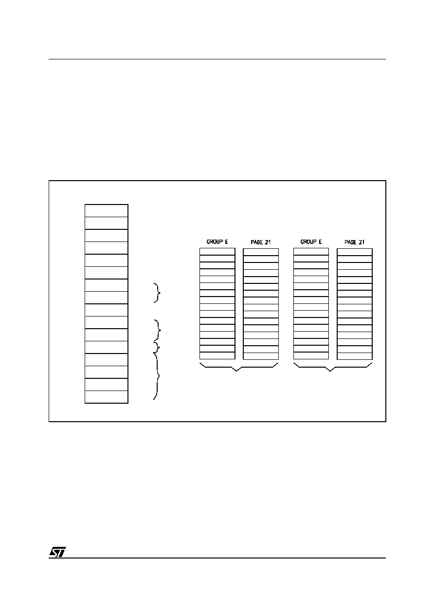
39/230
ST92163 - DEVICE ARCHITECTURE
2.5 MEMORY MANAGEMENT UNIT
The CPU Core includes a Memory Management
Unit (MMU) which must be programmed to per-
form memory accesses (even if external memory
is not used).
The MMU is controlled by 7 registers and 2 bits
(ENCSR and DPRREM) present in EMR2, which
may be written and read by the user program.
These registers are mapped within group F, Page
21 of the Register File. The 7 registers may be
sub-divided into 2 main groups: a first group of four
8-bit registers (DPR[3:0]), and a second group of
three 6-bit registers (CSR, ISR, and DMASR). The
first group is used to extend the address during
Data Memory access (DPR[3:0]). The second is
used to manage Program and Data Memory ac-
cesses during Code execution (CSR), Interrupts
Service Routines (ISR or CSR), and DMA trans-
fers (DMASR or ISR).
Figure 15. Page 21 Registers
DMASR
ISR
EMR2
EMR1
CSR
DPR3
DPR2
DPR1
DPR0
R255
R254
R253
R252
R251
R250
R249
R248
R247
R246
R245
R244
R243
R242
R241
R240
FFh
FEh
FDh
FCh
FBh
FAh
F9h
F8h
F7h
F6h
F5h
F4h
F3h
F2h
F1h
F0h
MMU
EM
Page 21
MMU
MMU
Bit DPRREM=0
SSPLR
SSPHR
USPLR
USPHR
MODER
PPR
RP1
RP0
FLAGR
CICR
P5DR
P4DR
P3DR
P2DR
P1DR
P0DR
DMASR
ISR
EMR2
EMR1
CSR
DPR3
DPR2
1
DPR0
Bit DPRREM=1
SSPLR
SSPHR
USPLR
USPHR
MODER
PPR
RP1
RP0
FLAGR
CICR
P5DR
P4DR
P3DR
P2DR
P1DR
P0DR
DMASR
ISR
EMR2
EMR1
CSR
DPR3
DPR2
DPR1
DPR0
Relocation of P[3:0] and DPR[3:0] Registers
(default setting)

40/230
ST92163 - DEVICE ARCHITECTURE
2.6 ADDRESS SPACE EXTENSION
To manage 4 Mbytes of addressing space, it is
necessary to have 22 address bits. The MMU
adds 6 bits to the usual 16-bit address, thus trans-
lating a 16-bit virtual address into a 22-bit physical
address. There are 2 different ways to do this de-
pending on the memory involved and on the oper-
ation being performed.
2.6.1 Addressing 16-Kbyte Pages
This extension mode is implicitly used to address
Data memory space if no DMA is being performed.
The Data memory space is divided into 4 pages of
16 Kbytes. Each one of the four 8-bit registers
(DPR[3:0], Data Page Registers) selects a differ-
ent 16-Kbyte page. The DPR registers allow ac-
cess to the entire memory space which contains
256 pages of 16 Kbytes.
Data paging is performed by extending the 14 LSB
of the 16-bit address with the contents of a DPR
register. The two MSBs of the 16-bit address are
interpreted as the identification number of the DPR
register to be used. Therefore, the DPR registers
are involved in the following virtual address rang-
es:
DPR0: from 0000h to 3FFFh;
DPR1: from 4000h to 7FFFh;
DPR2: from 8000h to BFFFh;
DPR3: from C000h to FFFFh.
The contents of the selected DPR register specify
one of the 256 possible data memory pages. This
8-bit data page number, in addition to the remain-
ing 14-bit page offset address forms the physical
22-bit address (see
Figure 10
).
A DPR register cannot be modified via an address-
ing mode that uses the same DPR register. For in-
stance, the instruction "POPW DPR0" is legal only
if the stack is kept either in the register file or in a
memory location above 8000h, where DPR2 and
DPR3 are used. Otherwise, since DPR0 and
DPR1 are modified by the instruction, unpredicta-
ble behaviour could result.
Figure 16. Addressing via DPR[3:0]
DPR0
DPR1
DPR2
DPR3
00
01
10
11
16-bit virtual address
22-bit physical address
8 bits
MMU registers
2 M
SB
14 LSB
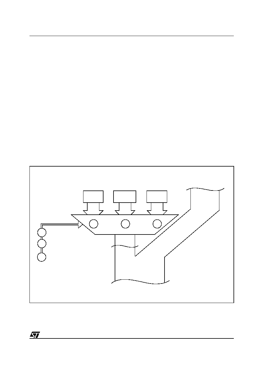
41/230
ST92163 - DEVICE ARCHITECTURE
ADDRESS SPACE EXTENSION (Cont'd)
2.6.2 Addressing 64-Kbyte Segments
This extension mode is used to address Data
memory space during a DMA and Program mem-
ory space during any code execution (normal code
and interrupt routines).
Three registers are used: CSR, ISR, and DMASR.
The 6-bit contents of one of the registers CSR,
ISR, or DMASR define one out of 64 Memory seg-
ments of 64 Kbytes within the 4 Mbytes address
space. The register contents represent the 6
MSBs of the memory address, whereas the 16
LSBs of the address (intra-segment address) are
given by the virtual 16-bit address (see
Figure 11
).
2.7 MMU REGISTERS
The MMU uses 7 registers mapped into Group F,
Page 21 of the Register File and 2 bits of the
EMR2 register.
Most of these registers do not have a default value
after reset.
2.7.1 DPR[3:0]: Data Page Registers
The DPR[3:0] registers allow access to the entire 4
Mbyte memory space composed of 256 pages of
16 Kbytes.
2.7.1.1 Data Page Register Relocation
If these registers are to be used frequently, they
may be relocated in register group E, by program-
ming bit 5 of the EMR2-R246 register in page 21. If
this bit is set, the DPR[3:0] registers are located at
R224-227 in place of the Port 0-3 Data Registers,
which are re-mapped to the default DPR's loca-
tions: R240-243 page 21.
Data Page Register relocation is illustrated in
Fig-
ure 9
.
Figure 17. Addressing via CSR, ISR, and DMASR
Fetching program
Data Memory
Fetching interrupt
instruction
accessed in DMA
instruction or DMA
access to Program
Memory
16-bit virtual address
22-bit physical address
6 bits
MMU registers
CSR
ISR
DMASR
1
2
3
1
2
3

42/230
ST92163 - DEVICE ARCHITECTURE
MMU REGISTERS (Cont'd)
DATA PAGE REGISTER 0 (DPR0)
R240 - Read/Write
Register Page: 21
Reset value: undefined
This register is relocated to R224 if EMR2.5 is set.
Bits 7:0 = DPR0_[7:0]: These bits define the 16-
Kbyte Data Memory page number. They are used
as the most significant address bits (A21-14) to ex-
tend the address during a Data Memory access.
The DPR0 register is used when addressing the
virtual address range 0000h-3FFFh.
DATA PAGE REGISTER 1 (DPR1)
R241 - Read/Write
Register Page: 21
Reset value: undefined
This register is relocated to R225 if EMR2.5 is set.
Bits 7:0 = DPR1_[7:0]: These bits define the 16-
Kbyte Data Memory page number. They are used
as the most significant address bits (A21-14) to ex-
tend the address during a Data Memory access.
The DPR1 register is used when addressing the
virtual address range 4000h-7FFFh.
DATA PAGE REGISTER 2 (DPR2)
R242 - Read/Write
Register Page: 21
Reset value: undefined
This register is relocated to R226 if EMR2.5 is set.
Bits 7:0 = DPR2_[7:0]: These bits define the 16-
Kbyte Data memory page. They are used as the
most significant address bits (A21-14) to extend
the address during a Data memory access. The
DPR2 register is involved when the virtual address
is in the range 8000h-BFFFh.
DATA PAGE REGISTER 3 (DPR3)
R243 - Read/Write
Register Page: 21
Reset value: undefined
This register is relocated to R227 if EMR2.5 is set.
Bits 7:0 = DPR3_[7:0]: These bits define the 16-
Kbyte Data memory page. They are used as the
most significant address bits (A21-14) to extend
the address during a Data memory access. The
DPR3 register is involved when the virtual address
is in the range C000h-FFFFh.
7
0
DPR0_7 DPR0_6 DPR0_5 DPR0_4 DPR0_3 DPR0_2 DPR0_1 DPR0_0
7
0
DPR1_7 DPR1_6 DPR1_5 DPR1_4 DPR1_3 DPR1_2 DPR1_1 DPR1_0
7
0
DPR2_7 DPR2_6 DPR2_5 DPR2_4 DPR2_3 DPR2_2 DPR2_1 DPR2_0
7
0
DPR3_7 DPR3_6 DPR3_5 DPR3_4 DPR3_3 DPR3_2 DPR3_1 DPR3_0

43/230
ST92163 - DEVICE ARCHITECTURE
MMU REGISTERS (Cont'd)
2.7.2 CSR: Code Segment Register
This register selects the 64-Kbyte code segment
being used at run-time to access instructions. It
can also be used to access data if the
spm
instruc-
tion has been executed (or
ldpp, ldpd, lddp
).
Only the 6 LSBs of the CSR register are imple-
mented, and bits 6 and 7 are reserved. The CSR
register allows access to the entire memory space,
divided into 64 segments of 64 Kbytes.
To generate the 22-bit Program memory address,
the contents of the CSR register is directly used as
the 6 MSBs, and the 16-bit virtual address as the
16 LSBs.
Note: The CSR register should only be read and
not written for data operations (there are some ex-
ceptions which are documented in the following
paragraph). It is, however, modified either directly
by means of the
jps
and
calls
instructions, or
indirectly via the stack, by means of the
rets
in-
struction.
CODE SEGMENT REGISTER (CSR)
R244 - Read/Write
Register Page: 21
Reset value: 0000 0000 (00h)
Bits 7:6 = Reserved, keep in reset state.
Bits 5:0 = CSR_[5:0]: These bits define the 64-
Kbyte memory segment (among 64) which con-
tains the code being executed. These bits are
used as the most significant address bits (A21-16).
2.7.3 ISR: Interrupt Segment Register
INTERRUPT SEGMENT REGISTER (ISR)
R248 - Read/Write
Register Page: 21
Reset value: undefined
ISR and ENCSR bit (EMR2 register) are also de-
scribed in the chapter relating to Interrupts, please
refer to this description for further details.
Bits 7:6 = Reserved, keep in reset state.
Bits 5:0 = ISR_[5:0]: These bits define the 64-
Kbyte memory segment (among 64) which con-
tains the interrupt vector table and the code for in-
terrupt service routines and DMA transfers (when
the PS bit of the DAPR register is reset). These
bits are used as the most significant address bits
(A21-16). The ISR is used to extend the address
space in two cases:
≠ Whenever an interrupt occurs: ISR points to the
64-Kbyte memory segment containing the inter-
rupt vector table and the interrupt service routine
code. See also the Interrupts chapter.
≠ During DMA transactions between the peripheral
and memory when the PS bit of the DAPR regis-
ter is reset : ISR points to the 64 K-byte Memory
segment that will be involved in the DMA trans-
action.
2.7.4 DMASR: DMA Segment Register
DMA SEGMENT REGISTER (DMASR)
R249 - Read/Write
Register Page: 21
Reset value: undefined
Bits 7:6 = Reserved, keep in reset state.
Bits 5:0 = DMASR_[5:0]: These bits define the 64-
Kbyte Memory segment (among 64) used when a
DMA transaction is performed between the periph-
eral's data register and Memory, with the PS bit of
the DAPR register set. These bits are used as the
most significant address bits (A21-16). If the PS bit
is reset, the ISR register is used to extend the ad-
dress.
7
0
0
0
CSR_5
CSR_4
CSR_3
CSR_2
CSR_1
CSR_0
7
0
0
0
ISR_5 ISR_4 ISR_3 ISR_2 ISR_1
ISR_0
7
0
0
0
DMA
SR_5
DMA
SR_4
DMA
SR_3
DMA
SR_2
DMA
SR_1
DMA
SR_0
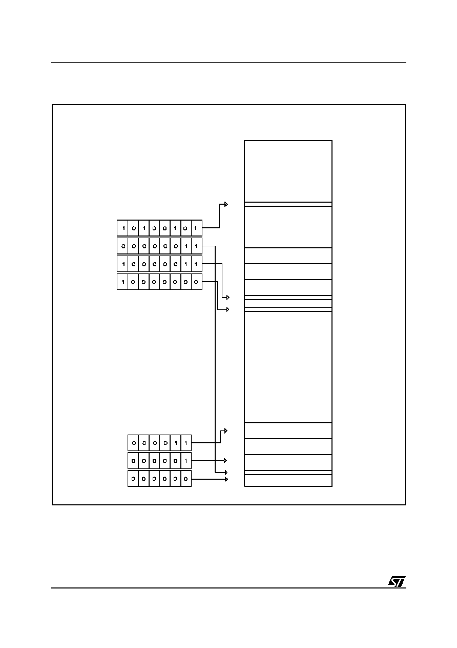
44/230
ST92163 - DEVICE ARCHITECTURE
MMU REGISTERS (Cont'd)
Figure 18. Memory Addressing Scheme (example)
3FFFFFh
294000h
240000h
23FFFFh
20C000h
200000h
1FFFFFh
040000h
03FFFFh
030000h
020000h
010000h
00C000h
000000h
DMASR
ISR
CSR
DPR3
DPR2
DPR1
DPR0
4M bytes
16K
16K
16K
64K
64K
64K
16K

45/230
ST92163 - DEVICE ARCHITECTURE
2.8 MMU USAGE
2.8.1 Normal Program Execution
Program memory is organized as a set of 64-
Kbyte segments. The program can span as many
segments as needed, but a procedure cannot
stretch across segment boundaries.
jps
,
calls
and
rets
instructions, which automatically modify
the CSR, must be used to jump across segment
boundaries. Writing to the CSR is forbidden during
normal program execution because it is not syn-
chronized with the opcode fetch. This could result
in fetching the first byte of an instruction from one
memory segment and the second byte from anoth-
er. Writing to the CSR is allowed when it is not be-
ing used, i.e during an interrupt service routine if
ENCSR is reset.
Note that a routine must always be called in the
same way, i.e. either always with
call
or always
with
calls
, depending on whether the routine
ends with
ret
or
rets
. This means that if the rou-
tine is written without prior knowledge of the loca-
tion of other routines which call it, and all the pro-
gram code does not fit into a single 64-Kbyte seg-
ment, then
calls
/
rets
should be used.
In typical microcontroller applications, less than 64
Kbytes of RAM are used, so the four Data space
pages are normally sufficient, and no change of
DPR[3:0] is needed during Program execution. It
may be useful however to map part of the ROM
into the data space if it contains strings, tables, bit
maps, etc.
If there is to be frequent use of paging, the user
can set bit 5 (DPRREM) in register R246 (EMR2)
of Page 21. This swaps the location of registers
DPR[3:0] with that of the data registers of Ports 0-
3. In this way, DPR registers can be accessed
without the need to save/set/restore the Page
Pointer Register. Port registers are therefore
moved to page 21. Applications that require a lot of
paging typically use more than 64 Kbytes of exter-
nal memory, and as ports 0, 1 and 2 are required
to address it, their data registers are unused.
2.8.2 Interrupts
The ISR register has been created so that the in-
terrupt routines may be found by means of the
same vector table even after a segment jump/call.
When an interrupt occurs, the CPU behaves in
one of 2 ways, depending on the value of the ENC-
SR bit in the EMR2 register (R246 on Page 21).
If this bit is reset (default condition), the CPU
works in original ST9 compatibility mode. For the
duration of the interrupt service routine, the ISR is
used instead of the CSR, and the interrupt stack
frame is kept exactly as in the original ST9 (only
the PC and flags are pushed). This avoids the
need to save the CSR on the stack in the case of
an interrupt, ensuring a fast interrupt response
time. The drawback is that it is not possible for an
interrupt service routine to perform segment
calls
/
jps
: these instructions would update the
CSR, which, in this case, is not used (ISR is used
instead). The code size of all interrupt service rou-
tines is thus limited to 64 Kbytes.
If, instead, bit 6 of the EMR2 register is set, the
ISR is used only to point to the interrupt vector ta-
ble and to initialize the CSR at the beginning of the
interrupt service routine: the old CSR is pushed
onto the stack together with the PC and the flags,
and then the CSR is loaded with the ISR. In this
case, an
iret
will also restore the CSR from the
stack. This approach lets interrupt service routines
access the whole 4-Mbyte address space. The
drawback is that the interrupt response time is
slightly increased, because of the need to also
save the CSR on the stack. Compatibility with the
original ST9 is also lost in this case, because the
interrupt stack frame is different; this difference,
however, would not be noticeable for a vast major-
ity of programs.
Data memory mapping is independent of the value
of bit 6 of the EMR2 register, and remains the
same as for normal code execution: the stack is
the same as that used by the main program, as in
the ST9. If the interrupt service routine needs to
access additional Data memory, it must save one
(or more) of the DPRs, load it with the needed
memory page and restore it before completion.
2.8.3 DMA
Depending on the PS bit in the DAPR register (see
DMA chapter) DMA uses either the ISR or the
DMASR for memory accesses: this guarantees
that a DMA will always find its memory seg-
ment(s), no matter what segment changes the ap-
plication has performed. Unlike interrupts, DMA
transactions cannot save/restore paging registers,
so a dedicated segment register (DMASR) has
been created. Having only one register of this kind
means that all DMA accesses should be pro-
grammed in one of the two following segments:
the one pointed to by the ISR (when the PS bit of
the DAPR register is reset), and the one refer-
enced by the DMASR (when the PS bit is set).

46/230
ST92163 - INTERRUPTS
3 INTERRUPTS
3.1 INTRODUCTION
The ST9 responds to peripheral and external
events through its interrupt channels. Current pro-
gram execution can be suspended to allow the
ST9 to execute a specific response routine when
such an event occurs, providing that interrupts
have been enabled, and according to a priority
mechanism. If an event generates a valid interrupt
request, the current program status is saved and
control passes to the appropriate Interrupt Service
Routine.
The ST9 CPU can receive requests from the fol-
lowing sources:
≠ On-chip peripherals
≠ External pins
≠ Top-Level Pseudo-non-maskable interrupt
According to the on-chip peripheral features, an
event occurrence can generate an Interrupt re-
quest which depends on the selected mode.
Up to eight external interrupt channels, with pro-
grammable input trigger edge, are available. In ad-
dition, a dedicated interrupt channel, set to the
Top-level priority, can be devoted either to the ex-
ternal NMI pin (where available) to provide a Non-
Maskable Interrupt, or to the Timer/Watchdog. In-
terrupt service routines are addressed through a
vector table mapped in Memory.
Figure 19. Interrupt Response
NORMAL
PROGRAM
FLOW
INTERRUPT
SERVICE
ROUTINE
IRET
INSTRUCTION
INTERRUPT
VR001833
CLEAR
PENDING BIT
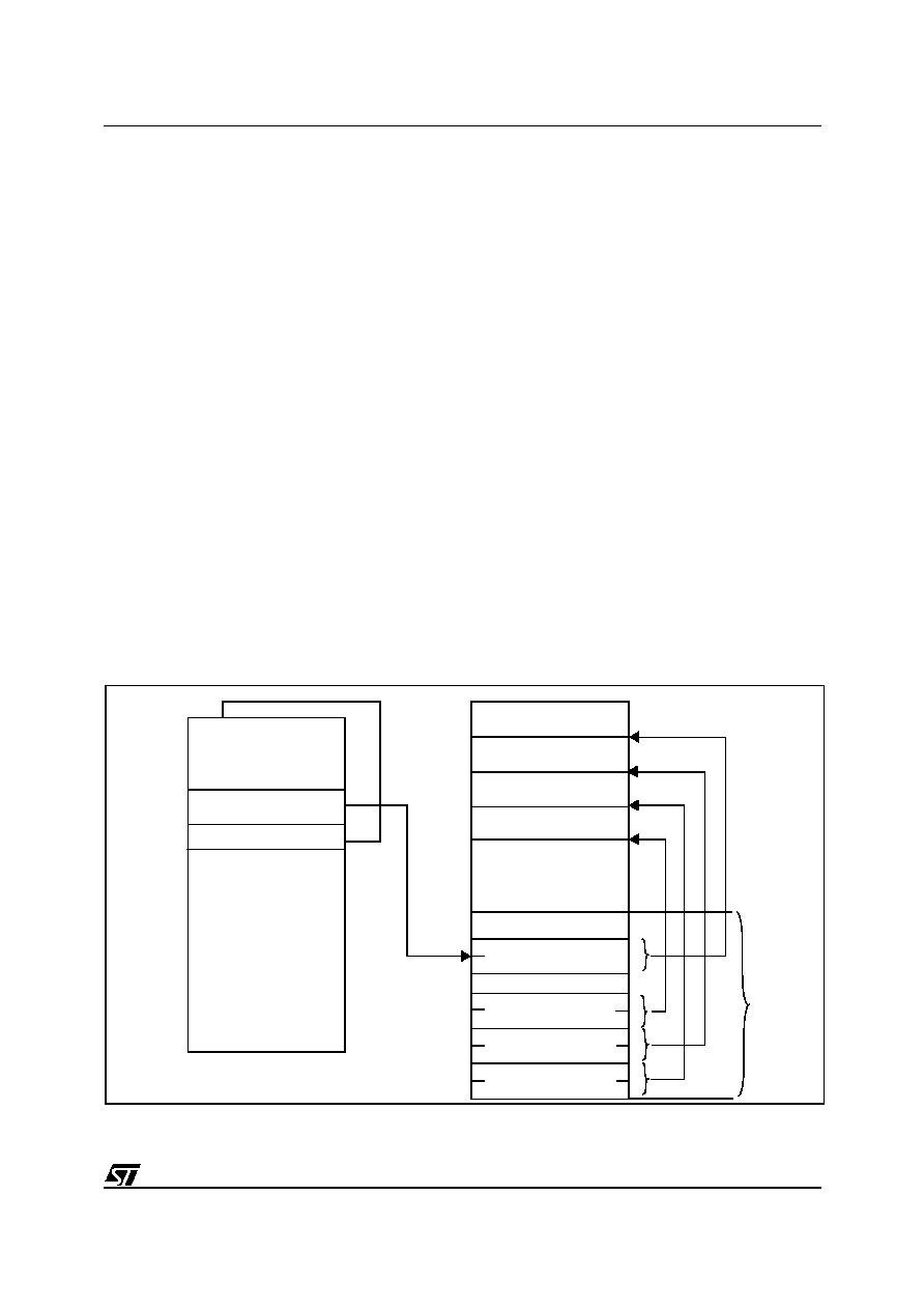
47/230
ST92163 - INTERRUPTS
INTERRUPTS (Cont'd)
3.2 INTERRUPT VECTORING
The ST9 implements an interrupt vectoring struc-
ture which allows the on-chip peripheral to identify
the location of the first instruction of the Interrupt
Service Routine automatically.
When an interrupt request is acknowledged, the
peripheral interrupt module provides, through its
Interrupt Vector Register (IVR), a vector to point
into the vector table of locations containing the
start addresses of the Interrupt Service Routines
(defined by the programmer).
Each peripheral has a specific IVR mapped within
its Register File pages.
The Interrupt Vector table, containing the address-
es of the Interrupt Service Routines, is located in
the first 256 locations of Memory pointed to by the
ISR register, thus allowing 8-bit vector addressing.
For a description of the ISR register refer to the
chapter describing the MMU.
The user Power on Reset vector is stored in the
first two physical bytes in memory, 000000h and
000001h.
The Top Level Interrupt vector is located at ad-
dresses 0004h and 0005h in the segment pointed
to by the Interrupt Segment Register (ISR).
With one Interrupt Vector register, it is possible to
address several interrupt service routines; in fact,
peripherals can share the same interrupt vector
register among several interrupt channels. The
most significant bits of the vector are user pro-
grammable to define the base vector address with-
in the vector table, the least significant bits are
controlled by the interrupt module, in hardware, to
select the appropriate vector.
Note: The first 256 locations of the memory seg-
ment pointed to by ISR can contain program code.
3.2.1 Divide by Zero trap
The Divide by Zero trap vector is located at ad-
dresses 0002h and 0003h of each code segment;
it should be noted that for each code segment a
Divide by Zero service routine is required.
Important
.
Although the Divide by Zero Trap oper-
ates as an interrupt, the FLAG Register is not
pushed onto the system Stack automatically. As a
result it must be regarded as a subroutine, and the
service routine must end with the
RET
instruction
(not
IRET
).
Figure 20. Interrupt Vector Table
USER ISR
PROGRAM MEMORY
POWER-ON RESET
DIVIDE-BY-ZERO
TOP LEVEL INT.
LO
LO
LO
HI
HI
HI
000000h
USER MAIN PROGRAM
USER TOP LEVEL ISR
USER DIVIDE-BY-ZERO ISR
0000FFh
VECTOR
TABLE
ISR ADDRESS
EVEN
ODD
INT. VECTOR REGISTER
LO
HI
REGISTER FILE
R240
R239
F PAGE REGISTERS
000002h
000004h

48/230
ST92163 - INTERRUPTS
INTERRUPTS (Cont'd)
3.2.2 Segment Paging During Interrupt
Routines
The ENCSR bit in the EMR2 register can be used
to select between original ST9 backward compati-
bility mode and ST9+ interrupt management
mode.
ST9 backward compatibility mode (ENCSR = 0)
If ENCSR is reset, the CPU works in original ST9
compatibility mode. For the duration of the inter-
rupt service routine, ISR is used instead of CSR,
and the interrupt stack frame is identical to that of
the original ST9: only the PC and Flags are
pushed.
This avoids saving the CSR on the stack in the
event of an interrupt, thus ensuring a faster inter-
rupt response time.
It is not possible for an interrupt service routine to
perform inter-segment calls or jumps: these in-
structions would update the CSR, which, in this
case, is not used (ISR is used instead). The code
segment size for all interrupt service routines is
thus limited to 64K bytes.
ST9+ mode (ENCSR = 1)
If ENCSR is set, ISR is only used to point to the in-
terrupt vector table and to initialize the CSR at the
beginning of the interrupt service routine: the old
CSR is pushed onto the stack together with the PC
and flags, and CSR is then loaded with the con-
tents of ISR.
In this case,
iret
will also restore CSR from the
stack. This approach allows interrupt service rou-
tines to access the entire 4 Mbytes of address
space. The drawback is that the interrupt response
time is slightly increased, because of the need to
also save CSR on the stack.
Full compatibility with the original ST9 is lost in this
case, because the interrupt stack frame is differ-
ent.
3.3 INTERRUPT PRIORITY LEVELS
The ST9 supports a fully programmable interrupt
priority structure. Nine priority levels are available
to define the channel priority relationships:
≠ The on-chip peripheral channels and the eight
external interrupt sources can be programmed
within eight priority levels. Each channel has a 3-
bit field, PRL (Priority Level), that defines its pri-
ority level in the range from 0 (highest priority) to
7 (lowest priority).
≠ The 9th level (Top Level Priority) is reserved for
the Timer/Watchdog or the External Pseudo
Non-Maskable Interrupt. An Interrupt service
routine at this level cannot be interrupted in any
arbitration mode. Its mask can be both maskable
(TLI) or non-maskable (TLNM).
3.4 PRIORITY LEVEL ARBITRATION
The 3 bits of CPL (Current Priority Level) in the
Central Interrupt Control Register contain the pri-
ority of the currently running program (CPU priori-
ty). CPL is set to 7 (lowest priority) upon reset and
can be modified during program execution either
by software or automatically by hardware accord-
ing to the selected Arbitration Mode.
During every instruction, an arbitration phase
takes place, during which, for every channel capa-
ble of generating an Interrupt, each priority level is
compared to all the other requests (interrupts or
DMA).
If the highest priority request is an interrupt, its
PRL value must be strictly lower (that is, higher pri-
ority) than the CPL value stored in the CICR regis-
ter (R230) in order to be acknowledged. The Top
Level Interrupt overrides every other priority.
3.4.1 Priority Level 7 (Lowest)
Interrupt requests at PRL level 7 cannot be ac-
knowledged, as this PRL value (the lowest possi-
ble priority) cannot be strictly lower than the CPL
value. This can be of use in a fully polled interrupt
environment.
3.4.2 Maximum Depth of Nesting
No more than 8 routines can be nested. If an inter-
rupt routine at level N is being serviced, no other
Interrupts located at level N can interrupt it. This
guarantees a maximum number of 8 nested levels
including the Top Level Interrupt request.
3.4.3 Simultaneous Interrupts
If two or more requests occur at the same time and
at the same priority level, an on-chip daisy chain,
specific to every ST9 version, selects the channel
ENCSR Bit
0
1
Mode
ST9 Compatible
ST9+
Pushed/Popped
Registers
PC, FLAGR
PC, FLAGR,
CSR
Max. Code Size
for interrupt
service routine
64KB
Within 1 segment
<4 MB
Across segments
49/230
ST92163 - INTERRUPTS
with the highest position in the chain, as shown in
Table 10
.
Table 10. Daisy Chain Priority
3.4.4 Dynamic Priority Level Modification
The main program and routines can be specifically
prioritized. Since the CPL is represented by 3 bits
in a read/write register, it is possible to modify dy-
namically the current priority value during program
execution. This means that a critical section can
have a higher priority with respect to other inter-
rupt requests. Furthermore it is possible to priori-
tize even the Main Program execution by modify-
ing the CPL during its execution. See
Figure 21
Figure 21. Example of Dynamic priority
level modification in Nested Mode
3.5 ARBITRATION MODES
The ST9 provides two interrupt arbitration modes:
Concurrent mode and Nested mode. Concurrent
mode is the standard interrupt arbitration mode.
Nested mode improves the effective interrupt re-
sponse time when service routine nesting is re-
quired, depending on the request priority levels.
The IAM control bit in the CICR Register selects
Concurrent Arbitration mode or Nested Arbitration
Mode.
3.5.1 Concurrent Mode
This mode is selected when the IAM bit is cleared
(reset condition). The arbitration phase, performed
during every instruction, selects the request with
the highest priority level. The CPL value is not
modified in this mode.
Start of Interrupt Routine
The interrupt cycle performs the following steps:
≠ All maskable interrupt requests are disabled by
clearing CICR.IEN.
≠ The PC low byte is pushed onto system stack.
≠ The PC high byte is pushed onto system stack.
≠ If ENCSR is set, CSR is pushed onto system
stack.
≠ The Flag register is pushed onto system stack.
≠ The PC is loaded with the 16-bit vector stored in
the Vector Table, pointed to by the IVR.
≠ If ENCSR is set, CSR is loaded with ISR con-
tents; otherwise ISR is used in place of CSR until
iret
instruction.
End of Interrupt Routine
The Interrupt Service Routine must be ended with
the
iret
instruction. The
iret
instruction exe-
cutes the following operations:
≠ The Flag register is popped from system stack.
≠ If ENCSR is set, CSR is popped from system
stack.
≠ The PC high byte is popped from system stack.
≠ The PC low byte is popped from system stack.
≠ All unmasked Interrupts are enabled by setting
the CICR.IEN bit.
≠ If ENCSR is reset, CSR is used instead of ISR.
Normal program execution thus resumes at the in-
terrupted instruction. All pending interrupts remain
pending until the next
ei
instruction (even if it is
executed during the interrupt service routine).
Note: In Concurrent mode, the source priority level
is only useful during the arbitration phase, where it
is compared with all other priority levels and with
the CPL. No trace is kept of its value during the
ISR. If other requests are issued during the inter-
rupt service routine, once the global CICR.IEN is
re-enabled, they will be acknowledged regardless
of the interrupt service routine's priority. This may
cause undesirable interrupt response sequences.
Highest Position
Lowest Position
INTA0
INTA1
INTB0
INTB1
INTC0
INTC1
INTD0
INTD1
USB
MFT
SCI
I2C
INT0/WDT
INT1/ADC
INT2
INT3
INT4/
INT5
INT6/RCCU
INT7/WKUP
6
5
4
7
Priority Level
MAIN
CPL is set to 5
CPL=7
MAIN
INT 6
CPL=6
INT6
ei
CPL is set to 7
CPL6 > CPL5:
INT6 pending
INTERRUPT 6 HAS PRIORITY LEVEL 6
by MAIN program
50/230
ST92163 - INTERRUPTS
ARBITRATION MODES (Cont'd)
Examples
In the following two examples, three interrupt re-
quests with different priority levels (2, 3 & 4) occur
simultaneously during the interrupt 5 service rou-
tine.
Example 1
In the first example, (simplest case,
Figure 22
) the
ei
instruction is not used within the interrupt serv-
ice routines. This means that no new interrupt can
be serviced in the middle of the current one. The
interrupt routines will thus be serviced one after
another, in the order of their priority, until the main
program eventually resumes.
Figure 22. Simple Example of a Sequence of Interrupt Requests with:
- Concurrent mode selected and
- IEN unchanged by the interrupt routines
6
5
4
3
2
1
0
7
Priority Level of
MAIN
INT 5
INT 2
INT 3
INT 4
MAIN
INT 5
INT 4
INT 3
INT 2
CPL is set to 7
CPL = 7
CPL = 7
CPL = 7
CPL = 7
CPL = 7
ei
INTERRUPT 2 HAS PRIORITY LEVEL 2
INTERRUPT 3 HAS PRIORITY LEVEL 3
INTERRUPT 4 HAS PRIORITY LEVEL 4
INTERRUPT 5 HAS PRIORITY LEVEL 5
Interrupt Request
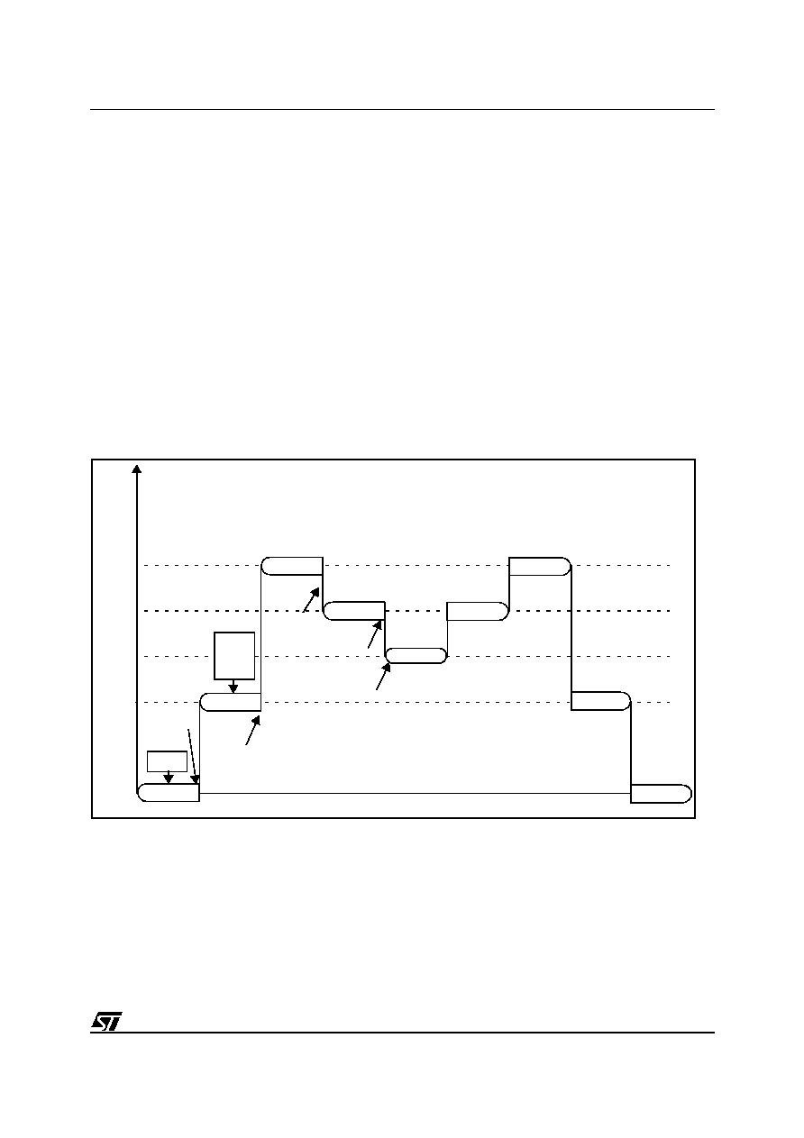
51/230
ST92163 - INTERRUPTS
ARBITRATION MODES (Cont'd)
Example 2
In the second example, (more complex,
Figure
23
), each interrupt service routine sets Interrupt
Enable with the
ei
instruction at the beginning of
the routine. Placed here, it minimizes response
time for requests with a higher priority than the one
being serviced.
The level 2 interrupt routine (with the highest prior-
ity) will be acknowledged first, then, when the
ei
instruction is executed, it will be interrupted by the
level 3 interrupt routine, which itself will be inter-
rupted by the level 4 interrupt routine. When the
level 4 interrupt routine is completed, the level 3 in-
terrupt routine resumes and finally the level 2 inter-
rupt routine. This results in the three interrupt serv-
ice routines being executed in the opposite order
of their priority.
It is therefore recommended to avoid inserting
the
ei
instruction in the interrupt service rou-
tine in Concurrent mode. Use the
ei
instruc-
tion only in nested mode.
IMPORTANT: If, in Concurrent Mode, interrupts
are nested (by executing
ei
in an interrupt service
routine), make sure that either ENCSR is set or
CSR=ISR, otherwise the
iret
of the innermost in-
terrupt will make the CPU use CSR instead of ISR
before the outermost interrupt service routine is
terminated, thus making the outermost routine fail.
Figure 23. Complex Example of a Sequence of Interrupt Requests with:
- Concurrent mode selected
- IEN set to 1 during interrupt service routine execution
6
5
4
3
2
1
0
7
MAIN
INT 5
INT 2
INT 3
INT 4
INT 5
INT 4
INT 3
INT 2
CPL is set to 7
CPL = 7
CPL = 7
CPL = 7
CPL = 7
CPL = 7
ei
INTERRUPT 2 HAS PRIORITY LEVEL 2
INTERRUPT 3 HAS PRIORITY LEVEL 3
INTERRUPT 4 HAS PRIORITY LEVEL 4
INTERRUPT 5 HAS PRIORITY LEVEL 5
INT 2
INT 3
CPL = 7
CPL = 7
INT 5
CPL = 7
MAIN
ei
ei
ei
Priority Level of
Interrupt Request
ei
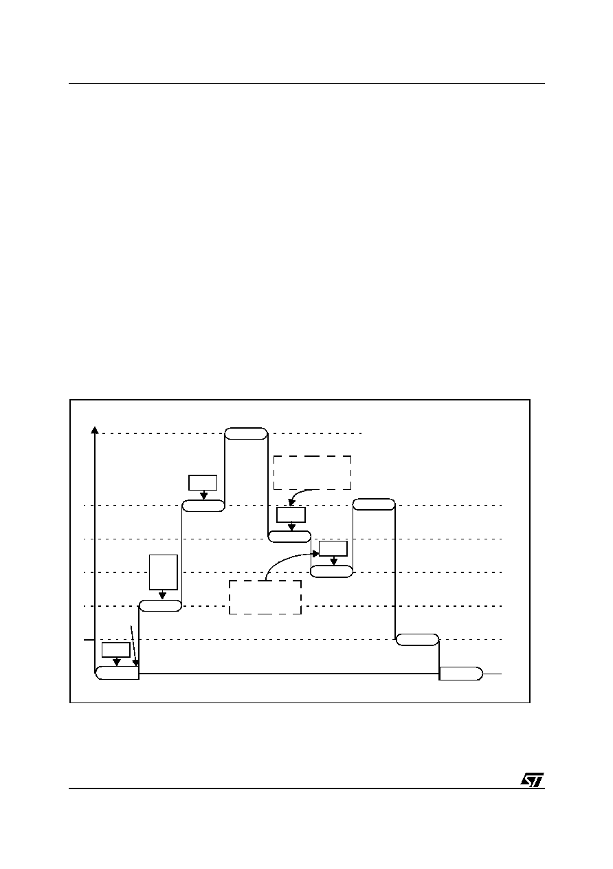
52/230
ST92163 - INTERRUPTS
ARBITRATION MODES (Cont'd)
3.5.2 Nested Mode
The difference between Nested mode and Con-
current mode, lies in the modification of the Cur-
rent Priority Level (CPL) during interrupt process-
ing.
The arbitration phase is basically identical to Con-
current mode, however, once the request is ac-
knowledged, the CPL is saved in the Nested Inter-
rupt Control Register (NICR) by setting the NICR
bit corresponding to the CPL value (i.e. if the CPL
is 3, the bit 3 will be set).
The CPL is then loaded with the priority of the re-
quest just acknowledged; the next arbitration cycle
is thus performed with reference to the priority of
the interrupt service routine currently being exe-
cuted.
Start of Interrupt Routine
The interrupt cycle performs the following steps:
≠ All maskable interrupt requests are disabled by
clearing CICR.IEN.
≠ CPL is saved in the special NICR stack to hold
the priority level of the suspended routine.
≠ Priority level of the acknowledged routine is
stored in CPL, so that the next request priority
will be compared with the one of the routine cur-
rently being serviced.
≠ The PC low byte is pushed onto system stack.
≠ The PC high byte is pushed onto system stack.
≠ If ENCSR is set, CSR is pushed onto system
stack.
≠ The Flag register is pushed onto system stack.
≠ The PC is loaded with the 16-bit vector stored in
the Vector Table, pointed to by the IVR.
≠ If ENCSR is set, CSR is loaded with ISR con-
tents; otherwise ISR is used in place of CSR until
iret
instruction.
Figure 24. Simple Example of a Sequence of Interrupt Requests with:
- Nested mode
- IEN unchanged by the interrupt routines
6
5
4
3
2
1
0
7
MAIN
INT 2
INT0
INT4
INT3
INT2
CPL is set to 7
CPL=2
CPL=7
ei
INTERRUPT 2 HAS PRIORITY LEVEL 2
INTERRUPT 3 HAS PRIORITY LEVEL 3
INTERRUPT 4 HAS PRIORITY LEVEL 4
INTERRUPT 5 HAS PRIORITY LEVEL 5
MAIN
INT 3
CPL=3
INT 6
CPL=6
INT5
INT 0
CPL=0
INT6
INT2
INTERRUPT 6 HAS PRIORITY LEVEL 6
INTERRUPT 0 HAS PRIORITY LEVEL 0
CPL6 > CPL3:
INT6 pending
CPL2 < CPL4:
Serviced next
INT 2
CPL=2
INT 4
CPL=4
INT 5
CPL=5
Priority Level of
Interrupt Request

53/230
ST92163 - INTERRUPTS
ARBITRATION MODES (Cont'd)
End of Interrupt Routine
The
iret
Interrupt Return instruction executes
the following steps:
≠ The Flag register is popped from system stack.
≠ If ENCSR is set, CSR is popped from system
stack.
≠ The PC high byte is popped from system stack.
≠ The PC low byte is popped from system stack.
≠ All unmasked Interrupts are enabled by setting
the CICR.IEN bit.
≠ The priority level of the interrupted routine is
popped from the special register (NICR) and
copied into CPL.
≠ If ENCSR is reset, CSR is used instead of ISR,
unless the program returns to another nested
routine.
The suspended routine thus resumes at the inter-
rupted instruction.
Figure 24
contains a simple example, showing that
if the
ei
instruction is not used in the interrupt
service routines, nested and concurrent modes
are equivalent.
Figure 25
contains a more complex example
showing how nested mode allows nested interrupt
processing (enabled inside the interrupt service
routines using the
ei
instruction) according to
their priority level.
Figure 25. Complex Example of a Sequence of Interrupt Requests with:
- Nested mode
- IEN set to 1 during the interrupt routine execution
INT 2
INT 3
CPL=3
INT 0
CPL=0
INT6
6
5
4
3
2
1
0
7
MAIN
INT 5
INT 4
INT0
INT4
INT3
INT2
CPL is set to 7
CPL=5
CPL=4
CPL=2
CPL=7
ei
INTERRUPT 2 HAS PRIORITY LEVEL 2
INTERRUPT 3 HAS PRIORITY LEVEL 3
INTERRUPT 4 HAS PRIORITY LEVEL 4
INTERRUPT 5 HAS PRIORITY LEVEL 5
INT 2
INT 4
CPL=2
CPL=4
INT 5
CPL=5
MAIN
ei
ei
INT 2
CPL=2
INT 6
CPL=6
INT5
INT2
ei
INTERRUPT 6 HAS PRIORITY LEVEL 6
INTERRUPT 0 HAS PRIORITY LEVEL 0
CPL6 > CPL3:
INT6 pending
CPL2 < CPL4:
Serviced just after ei
Priority Level of
Interrupt Request
ei
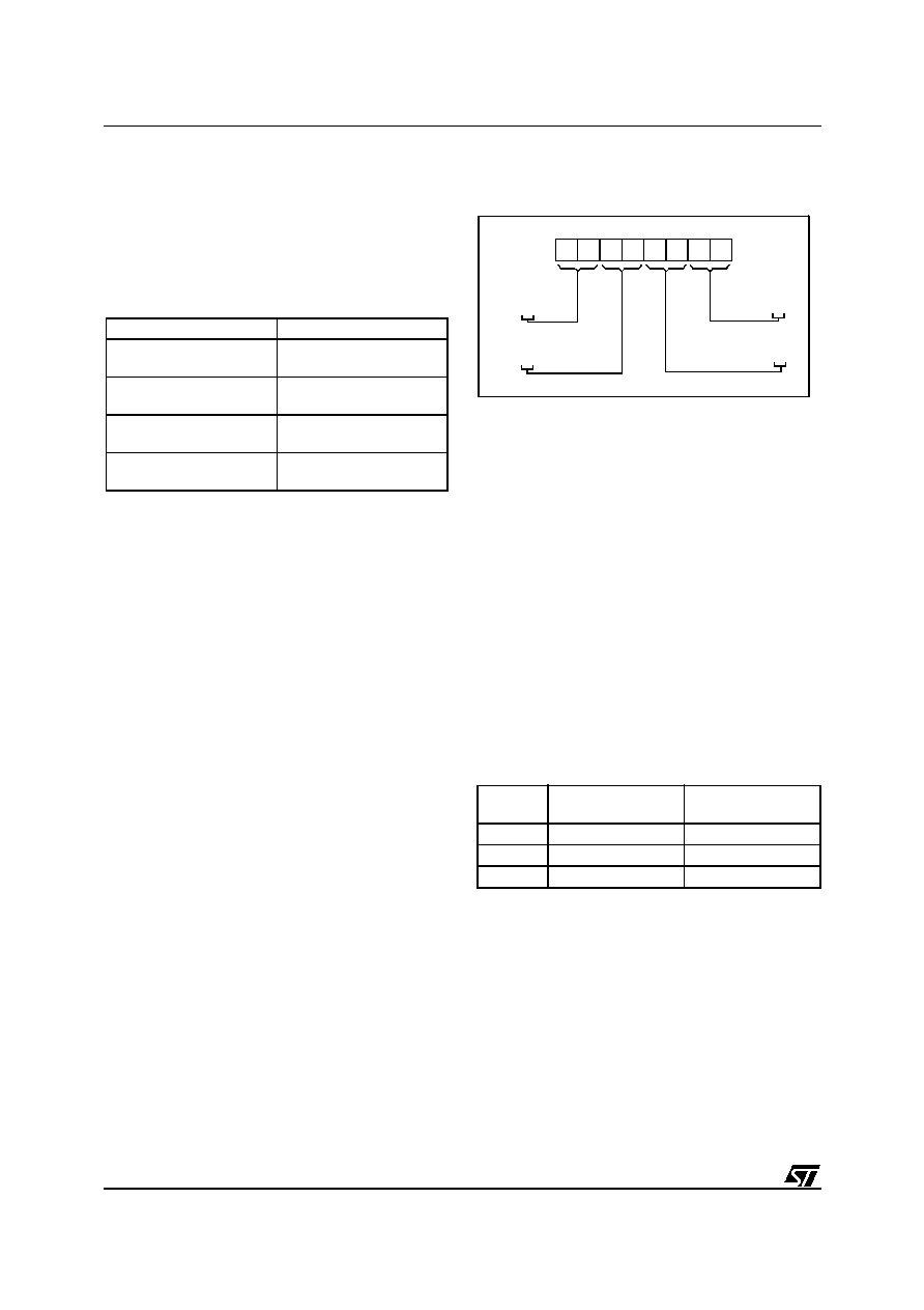
54/230
ST92163 - INTERRUPTS
3.6 EXTERNAL INTERRUPTS
The standard ST9 core contains 8 external inter-
rupts sources grouped into four pairs.
INT7 is connected to 8 different I/O pins of Port 3.
Once these pins are programmed as alternate
function they are able to generate an interrupt.
Table 11. External Interrupt Channel Grouping
INT0 .. 6 have a trigger control bit TEA0,..TED1
(R242,EITR.0,..,7 Page 0) to select triggering on
the rising or falling edge of the external pin. If the
Trigger control bit is set to "1", the corresponding
pending bit IPA0,..,IPD1 (R243, EIPR.0,..,6 Page
0) is set on the input pin rising edge, if it is cleared,
the pending bit is set on the falling edge of the in-
put pin. Each source can be individually masked
through the corresponding control bit
IMA0,..,IMD1 (EIMR.6,..,0). See
Figure 27
.
INT7 is falling edge sensitive only, bit EIMR.7 must
always be cleared.
The priority level of the external interrupt sources
can be programmed among the eight priority lev-
els with the control register EIPLR (R245). The pri-
ority level of each pair is software defined using
the bits PRL2, PRL1. For each pair, the even
channel (A0,B0,C0,D0) of the group has the even
priority level and the odd channel (A1,B1,C1,D1)
has the odd (lower) priority level.
Figure 26. Priority Level Examples
n
Figure 26
shows an example of priority levels.
Figure 27
gives an overview of the External inter-
rupt control bits and vectors.
≠ The source of the interrupt channel A0 can be
selected between the external pin INT0 (when
IA0S = "1", the reset value) or the On-chip Timer/
Watchdog peripheral (when IA0S = "0").
≠ The source of the interrupt channel A1 can be
selected between the external pin INT1 (when
AD-INT="0") or the on-chip ADC peripheral
(when AD-INT="1", the reset value).
≠ The source of the interrupt channel D0 can be
selected between the external pin INT6 (when
INT_SEL = "0") or the on-chip RCCU.
Important: When using channels shared by both
external interrupts and peripherals, special care
must be taken to configure their control registers
for both peripherals and interrupts.
Table 12. Multiplexed Interrupt Sources
External Interrupt
Channel
INT7
INT6
INTD1
INTD0
INT5
INT4
INTC1
INTC0
INT3
INT2
INTB1
INTB0
INT1
INT0
INTA1
INTA0
Channel
Internal Interrupt
Source
External Interrupt
Source
INTA0
Timer/Watchdog
INT0
INTA1
ADC
INT1
INTD0
RCCU
INT6
1
0
0
1
0
0
1
PL2D PL1D PL2C PL1C PL2B PL1B PL2A PL1A
INT.D1:
INT.C1: 001=1
INT.D0:
SOURCE
PRIORITY
PRIORITY
SOURCE
INT.A0: 010=2
INT.A1: 011=3
INT.B1: 101=5
INT.B0: 100=4
INT.C0: 000=0
EIPLR
VR000151
0
100=4
101=5
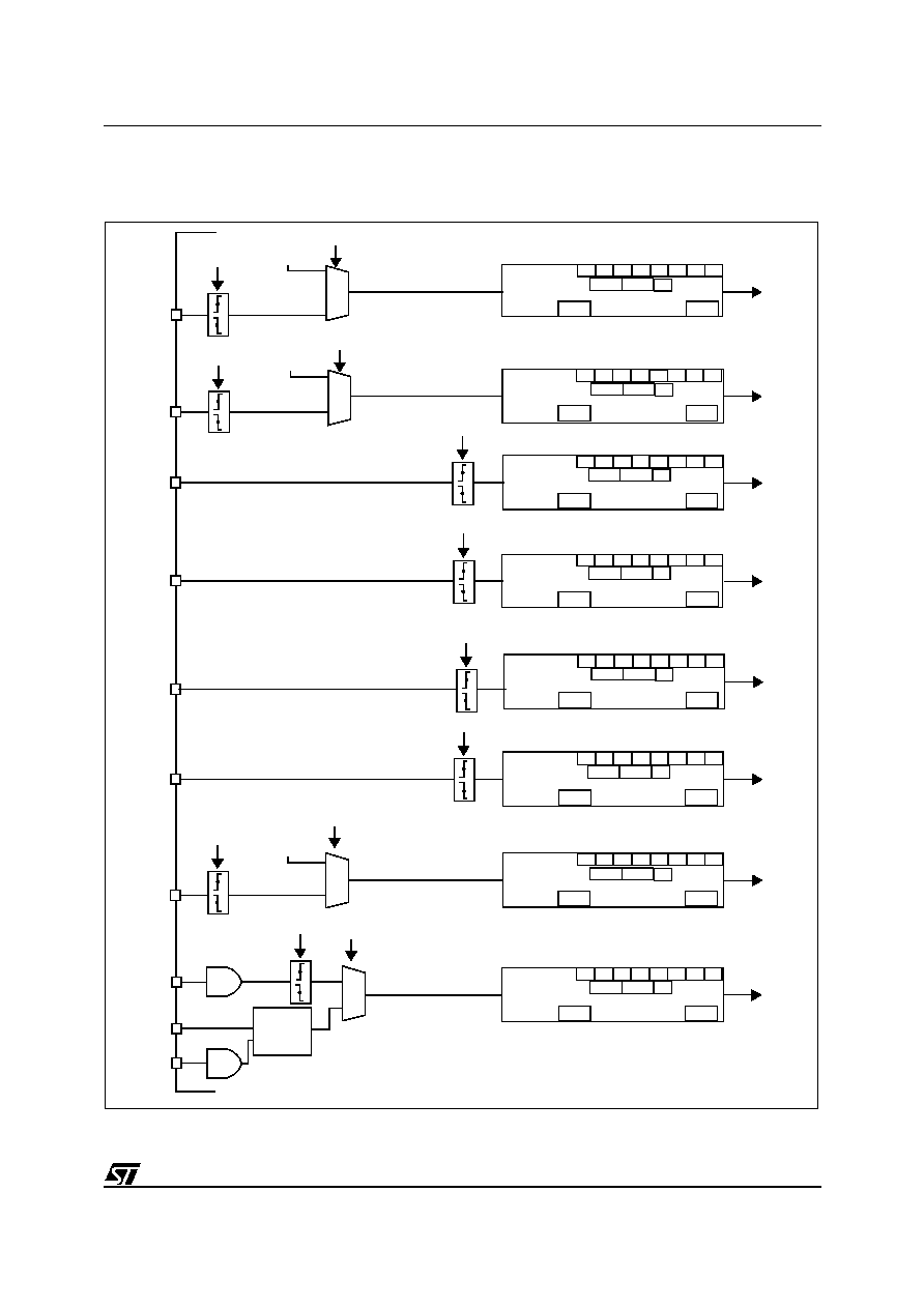
55/230
ST92163 - INTERRUPTS
EXTERNAL INTERRUPTS (Cont'd)
Figure 27. External Interrupts Control Bits and Vectors
INT A0
request
VECTOR
Priority level
Mask bit
Pending bit
IMA0
IPA0
V7 V6 V5 V4 0
0
0
X
"0"
"1"
IA0S
Watchdog/Timer
End of count
INT 0 pin
INT A1
request
TEA1
INT 1 pin
INT B0
request
INT 2 pin
INT B1
request
TEB1
INT 3 pin
INT C0
request
INT 4 pin
INT C1
request
TEC1
INT 5 pin
INT D0
request
TED0
INT 6 pin
INT D1
request
P3.[7:0]
VECTOR
Priority level
Mask bit
Pending bit
IMA1
IPA1
V7 V6 V5 V4 0
0
1
X
V7 V6 V5 V4 0
1
0
X
V7 V6 V5 V4 0
1
1
X
V7 V6 V5 V4 1
0
0
X
V7 V6 V5 V4 1
0
1
X
V7 V6 V5 V4 1
1
0
X
V7 V6 V5 V4 1
1
1
X
VECTOR
Priority level
VECTOR
Priority level
VECTOR
Priority level
VECTOR
Priority level
VECTOR
Priority level
VECTOR
Priority level
Mask bit
IMB0
Pending bit IPB0
Pending bit IPB1
Pending bit IPC0
Pending bit IPC1
Pending bit IPD0
Pending bit IPD1
Mask bit IMB1
Mask bit IMC0
Mask bit IMC1
Mask bit IMD0
Mask bit IMD1
* Shared channels, see warning
*
AD-INT
ADC
"1"
"0"
INT_SEL
RCCU
"1"
"0"
TEA0
TEC0
TEB0
*
*
INT 7 pins
0
PL2A PL1A
0
PL2B PL1B
1
PL2A PL1A
1
PL2B PL1B
0
PL2C PL1C
1
PL2C PL1C
0
PL2D PL1D
1
PL2D PL1D
"0"
"1"
ID1S
*
Wake-up
Controller
WKUP
[13:0] pins
TED1
WKUP14
P1.[7:0]
pins
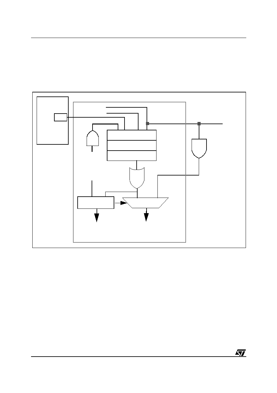
56/230
ST92163 - INTERRUPTS
3.7 MANAGEMENT OF WAKE-UP LINES AND EXTERNAL INTERRUPT LINES
In the ST92163, fifteen Wake-up lines
(WKUP[14:0]) are available on external pins. The
WKUP[15] line is internally connected to the USB
interface line.
Figure 28
shows the connections of the External
Interrupt Lines INT7[7:0] and the Wake-up/Inter-
rupt Lines managed through the WUIMU on the
INTD1 interrupt channel.
Figure 28. Wake-Up Lines and External Interrupt Lines Management
Trigger Registers
Pending Registers
Mask Registers
1
0
INT7[7:0]
WKUP[7:0]
WKUP[13:8]
(to CPU)
External Interrupt
WUIMU
STOP
SW Setting
WUCTRL Register
INTD1
(to RCCU)
ID1S bit
WKUP14
WKUP14[7:0]
USB
INTERFACE
WKUP15
ESUSP
USBISTR
Register
57/230
ST92163 - INTERRUPTS
3.8 TOP LEVEL INTERRUPT
The Top Level Interrupt channel can be assigned
either to the external pin NMI or to the Timer/
Watchdog according to the status of the control bit
EIVR.TLIS (R246.2, Page 0). If this bit is high (the
reset condition) the source is the external pin NMI.
If it is low, the source is the Timer/ Watchdog End
Of Count. When the source is the NMI external
pin, the control bit EIVR.TLTEV (R246.3; Page 0)
selects between the rising (if set) or falling (if reset)
edge generating the interrupt request. When the
selected event occurs, the CICR.TLIP bit (R230.6)
is set. Depending on the mask situation, a Top
Level Interrupt request may be generated. Two
kinds of masks are available, a Maskable mask
and a Non-Maskable mask. The first mask is the
CICR.TLI bit (R230.5): it can be set or cleared to
enable or disable respectively the Top Level Inter-
rupt request. If it is enabled, the global Enable In-
terrupt bit, CICR.IEN (R230.4; Page 0) must also
be enabled in order to allow a Top Level Request.
The second mask NICR.TLNM (R247.7; Page 0)
is a set-only mask. Once set, it enables the Top
Level Interrupt request independently of the value
of CICR.IEN and it cannot be cleared by the pro-
gram. Only the processor RESET cycle can clear
this bit. This does not prevent the user from ignor-
ing some sources due to a change in TLIS.
The Top Level Interrupt Service Routine cannot be
interrupted by any other interrupt or DMA request,
in any arbitration mode, not even by a subsequent
Top Level Interrupt request.
Warning. The interrupt machine cycle of the Top
Level Interrupt does not clear the CICR.IEN bit,
and the corresponding
iret
does not set it.
3.9 ON-CHIP PERIPHERAL INTERRUPTS
The general structure of the peripheral interrupt
unit is described here, however each on-chip pe-
ripheral has its own specific interrupt unit contain-
ing one or more interrupt channels, or DMA chan-
nels. Please refer to the specific peripheral chap-
ter for the description of its interrupt features and
control registers.
The on-chip peripheral interrupt channels provide
the following control bits:
≠ Interrupt Pending bit (IP). Set by hardware
when the Trigger Event occurs. Can be set/
cleared by software to generate/cancel pending
interrupts and give the status for Interrupt polling.
≠ Interrupt Mask bit (IM). If IM = "0", no interrupt
request is generated. If IM ="1" an interrupt re-
quest is generated whenever IP = "1" and
CICR.IEN = "1".
≠ Priority Level (PRL, 3 bits). These bits define
the current priority level, PRL=0: the highest pri-
ority, PRL=7: the lowest priority (the interrupt
cannot be acknowledged)
≠ Interrupt Vector Register (IVR, up to 7 bits).
The IVR points to the vector table which itself
contains the interrupt routine start address.
Figure 29. Top Level Interrupt Structure
WATCHDOG ENABLE
WDEN
WATCHDOG TIMER
END OF COUNT
NMI
OR
TLTEV
MUX
TLIS
TLIP
TLNM
TLI
IEN
PENDING
MASK
TOP LEVEL
INTERRUPT
VA00294
CORE
RESET
REQUEST

58/230
ST92163 - INTERRUPTS
3.10 INTERRUPT RESPONSE TIME
The interrupt arbitration protocol functions com-
pletely asynchronously from instruction flow, and
requires 6 CPUCLK cycles to resolve the request's
priority.
Requests are sampled every 5 CPUCLK cycles.
If the interrupt request comes from an external pin,
the trigger event must occur a minimum of one
INTCLK cycle before the sampling time.
When an arbitration results in an interrupt request
being generated, the interrupt logic checks if the
current instruction (which could be at any stage of
execution) can be safely aborted; if this is the
case, instruction execution is terminated immedi-
ately and the interrupt request is serviced; if not,
the CPU waits until the current instruction is termi-
nated and then services the request. Instruction
execution can normally be aborted provided no
write operation has been performed.
For an interrupt deriving from an external interrupt
channel, the response time between a user event
and the start of the interrupt service routine can
range from a minimum of 26 clock cycles to a max-
imum of 48 clock cycles.
For a non-maskable Top Level interrupt, the re-
sponse time between a user event and the start of
the interrupt service routine can range from a min-
imum of 22 clock cycles to a maximum of 48 clock
cycles.
In order to guarantee edge detection, input signals
must be kept low/high for a minimum of one
INTCLK cycle.
An interrupt machine cycle requires a basic 18 in-
ternal clock cycles (CPUCLK), to which must be
added a further 2 clock cycles if the stack is in the
Register File. 2 more clock cycles must further be
added if the CSR is pushed (ENCSR =1).
The interrupt machine cycle duration forms part of
the two examples of interrupt response time previ-
ously quoted; it includes the time required to push
values on the stack, as well as interrupt vector
handling.
In Wait for Interrupt mode, a further cycle is re-
quired as wake-up delay.

59/230
ST92163 - INTERRUPTS
3.11 INTERRUPT REGISTERS
CENTRAL INTERRUPT CONTROL REGISTER
(CICR)
R230 - Read/Write
Register Page: System
Reset value: 1000 0111 (87h)
Bit 7 = GCEN:
Global Counter Enable.
This bit enables the 16-bit Multifunction Timer pe-
ripheral.
0: MFT disabled
1: MFT enabled
Bit 6 = TLIP:
Top Level Interrupt Pending
.
This bit is set by hardware when Top Level Inter-
rupt (TLI) trigger event occurs. It is cleared by
hardware when a TLI is acknowledged. It can also
be set by software to implement a software TLI.
0: No TLI pending
1: TLI pending
Bit 5 = TLI:
Top Level Interrupt.
This bit is set and cleared by software.
0: Generate a Top Level Interrupt only if TLNM=1
1: Generate a Top Level Interrupt request when
the IEN
and TLIP bits=1.
Bit 4 = IEN:
Interrupt Enable
.
This bit is cleared by the interrupt machine cycle
(except for a TLI).
It is set by the
iret
instruction (except for a return
from TLI).
It is set by the
EI
instruction.
It is cleared by the
DI
instruction.
0: Maskable interrupts disabled
1: Maskable Interrupts enabled
Note: The IEN bit can also be changed by soft-
ware using any instruction that operates on regis-
ter CICR, however in this case, take care to avoid
spurious interrupts, since IEN cannot be cleared in
the middle of an interrupt arbitration. Only modify
the IEN bit when interrupts are disabled or when
no peripheral can generate interrupts. For exam-
ple, if the state of IEN is not known in advance,
and its value must be restored from a previous
push of CICR on the stack, use the sequence
DI;
POP CICR
to make sure that no interrupts are be-
ing arbitrated when CICR is modified.
Bit 3 = IAM:
Interrupt Arbitration Mode
.
This bit is set and cleared by software.
0: Concurrent Mode
1: Nested Mode
Bits 2:0 = CPL[2:0]:
Current Priority Level
.
These bits define the Current Priority Level.
CPL=0 is the highest priority. CPL=7 is the lowest
priority. These bits may be modified directly by the
interrupt hardware when Nested Interrupt Mode is
used.
EXTERNAL INTERRUPT TRIGGER REGISTER
(EITR)
R242 - Read/Write
Register Page: 0
Reset value: 0000 0000 (00h)
Bit 7 = TED1:
INTD1 Trigger Event
Must always stay cleared
Bit 6 = TED0:
INTD0 Trigger Event
Bit 5 = TEC1:
INTC1 Trigger Event
Bit 4 = TEC0:
INTC0 Trigger Event
Bit 3 = TEB1:
INTB1 Trigger Event
Bit 2 = TEB0:
INTB0 Trigger Event
Bit 1 = TEA1:
INTA1 Trigger Event
Bit 0 = TEA0:
INTA0 Trigger Event
These bits are set and cleared by software.
0: Select falling edge as interrupt trigger event
1: Select rising edge as interrupt trigger event
7
0
GCEN TLIP
TLI
IEN
IAM
CPL2 CPL1 CPL0
7
0
TED1 TED0 TEC1 TEC0 TEB1 TEB0 TEA1 TEA0
60/230
ST92163 - INTERRUPTS
INTERRUPT REGISTERS (Cont'd)
EXTERNAL INTERRUPT PENDING REGISTER
(EIPR)
R243 - Read/Write
Register Page: 0
Reset value: 0000 0000 (00h)
Bit 7 = IPD1:
INTD1
Interrupt Pending bit
Bit
6 = IPD0:
INTD0
Interrupt Pending bit
Bit 5 = IPC1:
INTC1 Interrupt Pending bit
Bit 4 = IPC0:
INTC0
Interrupt Pending bit
Bit 3 = IPB1:
INTB1
Interrupt Pending bit
Bit 2 = IPB0:
INTB0 Interrupt Pending bit
Bit 1 = IPA1:
INTA1
Interrupt Pending bit
Bit 0 = IPA0:
INTA0 Interrupt Pending bit
These bits are set by hardware on occurrence of a
trigger event (as specified in the EITR register)
and are cleared by hardware on interrupt acknowl-
edge. They can also be set by software to imple-
ment a software interrupt.
0: No interrupt pending
1: Interrupt pending
EXTERNAL INTERRUPT MASK-BIT REGISTER
(EIMR)
R244 - Read/Write
Register Page: 0
Reset value: 0000 0000 (00h)
Bit 7 = IMD1:
INTD1 Interrupt Mask
Bit 6 = IMD0:
INTD0 Interrupt Mask
Bit 5 = IMC1:
INTC1 Interrupt Mask
Bit
4 = IMC0:
INTC0 Interrupt Mask
Bit 3 = IMB1:
INTB1 Interrupt Mask
Bit 2 = IMB0:
INTB0 Interrupt Mask
Bit
1 = IMA1:
INTA1 Interrupt Mask
Bit 0 = IMA0:
INTA0 Interrupt Mask
These bits are set and cleared by software.
0: Interrupt masked
1: Interrupt not masked (an interrupt is generated if
the IPxx and IEN bits = 1)
EXTERNAL INTERRUPT PRIORITY LEVEL
REGISTER (EIPLR)
R245 - Read/Write
Register Page: 0
Reset value: 1111 1111 (FFh)
Bits 7:6 = PL2D, PL1D:
INTD0, D1 Priority Level.
Bits 5:4 = PL2C, PL1C:
INTC0, C1 Priority Level.
Bits 3:2 = PL2B, PL1B:
INTB0, B1 Priority Level.
Bits 1:0 = PL2A, PL1A:
INTA0, A1 Priority Level.
These bits are set and cleared by software.
The priority is a three-bit value. The LSB is fixed by
hardware at 0 for Channels A0, B0, C0 and D0 and
at 1 for Channels A1, B1, C1 and D1.
7
0
IPD1
IPD0
IPC1
IPC0
IPB1
IPB0
IPA1
IPA0
7
0
IMD1 IMD0 IMC1 IMC0 IMB1 IMB0 IMA1 IMA0
7
0
PL2D PL1D PL2C PL1C PL2B PL1B PL2A PL1A
PL2x
PL1x
Hardware
bit
Priority
0
0
0
1
0 (Highest)
1
0
1
0
1
2
3
1
0
0
1
4
5
1
1
0
1
6
7 (Lowest)

61/230
ST92163 - INTERRUPTS
INTERRUPT REGISTERS (Cont'd)
EXTERNAL INTERRUPT VECTOR REGISTER
(EIVR)
R246 - Read/Write
Register Page: 0
Reset value: xxxx 0110 (x6h)
Bits 7:4 = V[7:4]:
Most significant nibble of Exter-
nal Interrupt Vector
.
These bits are not initialized by reset. For a repre-
sentation of how the full vector is generated from
V[7:4] and the selected external interrupt channel,
refer to
Figure 27
.
Bit 3 = TLTEV:
Top Level Trigger Event bit.
This bit is set and cleared by software.
0: Select falling edge as NMI trigger event
1: Select rising edge as NMI trigger event
Bit 2 = TLIS:
Top Level Input Selection
.
This bit is set and cleared by software.
0: Watchdog End of Count is TL interrupt source
1: NMI is TL interrupt source
Bit 1 = IA0S:
Interrupt Channel A0 Selection.
This bit is set and cleared by software.
0: Watchdog End of Count is INTA0 source
1: External Interrupt pin is INTA0 source
Bit 0 = EWEN:
External Wait Enable.
This bit is set and cleared by software.
0: WAITN pin disabled
1: WAITN pin enabled (to stretch the external
memory access cycle).
Note: For more details on Wait mode refer to the
section describing the WAITN pin in the External
Memory Chapter.
NESTED INTERRUPT CONTROL (NICR)
R247 - Read/Write
Register Page: 0
Reset value: 0000 0000 (00h)
Bit 7 = TLNM:
Top Level Not Maskable
.
This bit is set by software and cleared only by a
hardware reset.
0: Top Level Interrupt Maskable. A top level re-
quest is generated if the IEN, TLI and TLIP bits
=1
1: Top Level Interrupt Not Maskable. A top level
request is generated if the TLIP bit =1
Bits 6:0 = HL[6:0]:
Hold Level
x
These bits are set by hardware when, in Nested
Mode, an interrupt service routine at level x is in-
terrupted from a request with higher priority (other
than the Top Level interrupt request). They are
cleared by hardware at the
iret
execution when
the routine at level x is recovered.
7
0
V7
V6
V5
V4
TLTEV TLIS IAOS EWEN
7
0
TLNM HL6
HL5
HL4
HL3
HL2
HL1
HL0

62/230
ST92163 - INTERRUPTS
INTERRUPT REGISTERS (Cont'd)
EXTERNAL MEMORY REGISTER 2 (EMR2)
R246 - Read/Write
Register Page: 21
Reset value: 0000 1111 (0Fh)
Bits 7, 5:0 = Reserved, keep in reset state. Refer
to the external Memory Interface Chapter.
Bit 6 = ENCSR:
Enable Code Segment Register.
This bit is set and cleared by software. It affects
the ST9 CPU behaviour whenever an interrupt re-
quest is issued.
0: The CPU works in original ST9 compatibility
mode. For the duration of the interrupt service
routine, ISR is used instead of CSR, and the in-
terrupt stack frame is identical to that of the orig-
inal ST9: only the PC and Flags are pushed.
This avoids saving the CSR on the stack in the
event of an interrupt, thus ensuring a faster in-
terrupt response time. The drawback is that it is
not possible for an interrupt service routine to
perform inter-segment calls or jumps: these in-
structions would update the CSR, which, in this
case, is not used (ISR is used instead). The
code segment size for all interrupt service rou-
tines is thus limited to 64K bytes.
1: ISR is only used to point to the interrupt vector
table and to initialize the CSR at the beginning
of the interrupt service routine: the old CSR is
pushed onto the stack together with the PC and
flags, and CSR is then loaded with the contents
of ISR. In this case,
iret
will also restore the
CSR from the stack. This approach allows inter-
rupt service routines to access the entire 4
Mbytes of address space; the drawback is that
the interrupt response time is slightly increased,
because of the need to also save the CSR on
the stack. Full compatibility with the original ST9
is lost in this case, because the interrupt stack
frame is different; this difference, however,
should not affect the vast majority of programs.
7
0
0
ENCSR
0
0
1
1
1
1
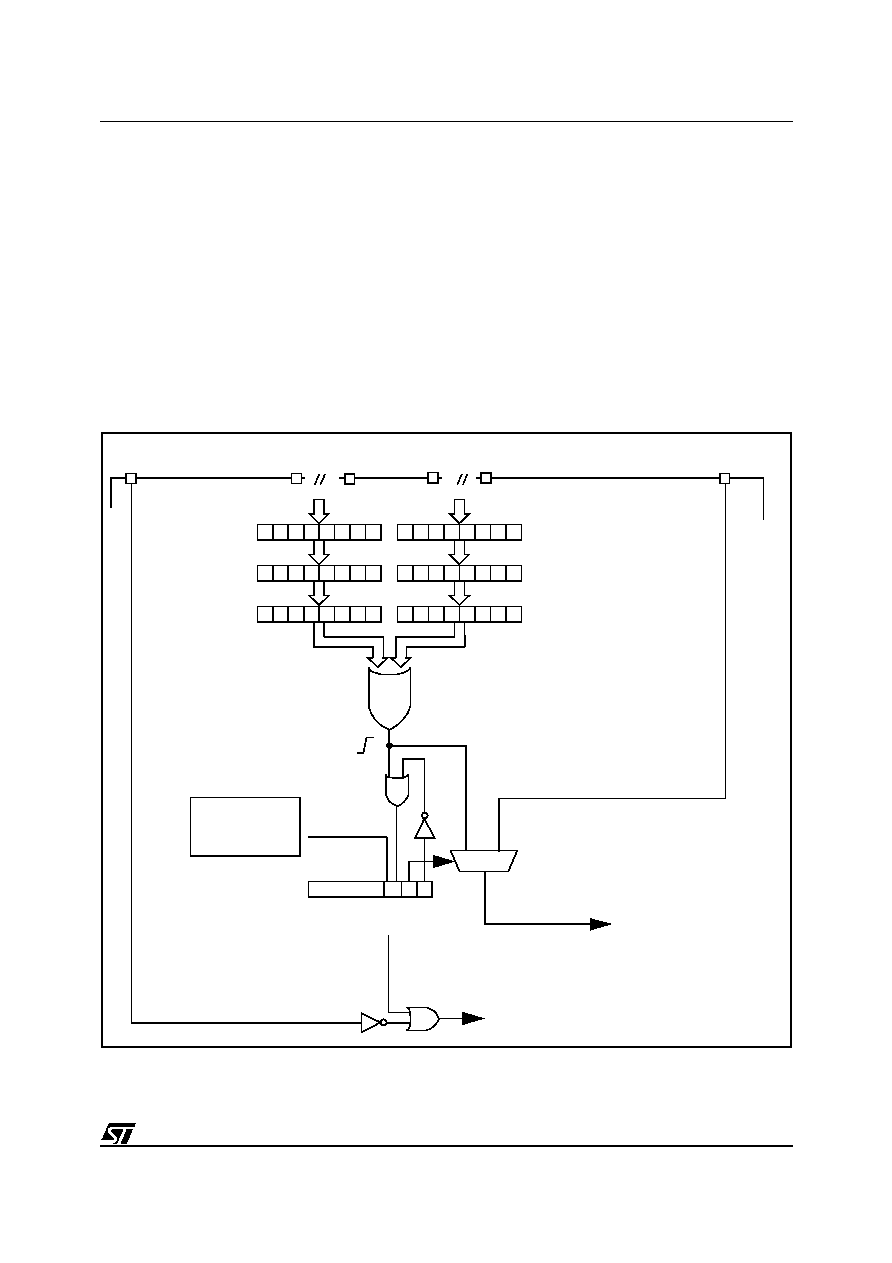
63/230
ST92163 - INTERRUPTS
3.12 WAKE-UP / INTERRUPT LINES MANAGEMENT UNIT (WUIMU)
3.12.1 Introduction
The Wake-up/Interrupt Management Unit extends
the number of external interrupt lines from 8 to 23
(depending on the number of external interrupt
lines mapped on external pins of the device). It al-
lows the source of the INTD1 external interrupt
channel to be selected between the INT7 pin and
up to 16 additional external Wake-up/interrupt
pins.
These 16 WKUP pins can be programmed as ex-
ternal interrupt lines or as wake-up lines, able to
exit the microcontroller from low power mode
(STOP mode) (see
Figure 30
).
3.12.2 Main Features
s
Supports up to 16 additional external wake-up
or interrupt lines
s
Wake-Up lines can be used to wake-up the ST9
from STOP mode.
s
Programmable selection of wake-up or interrupt
s
Programmable wake-up trigger edge polarity
s
All Wake-Up Lines maskable
Note: The number of available pins is device de-
pendent. Refer to the device pinout description.
Figure 30. Wake-Up Lines / Interrupt Management Unit Block Diagram
WUTRH
WUTRL
WUPRH
WUPRL
WUMRH
WUMRL
TRIGGERING LEVEL REGISTERS
PENDING REQUEST REGISTERS
MASK REGISTERS
WKUP[7:0]
WKUP[15:8]
1
0
Se
t
WUCTRL
SW SETTING
WK
UP
-
I
N
T
ID
1
S
ST
O
P
Re
se
t
TO RCCU - Stop Mode Control
TO CPU
INTD1 - External Interrupt Channel
INT7
STOP
Note: Reset Signal
on stop bit is
stronger than
the set signal

64/230
ST92163 - INTERRUPTS
WAKE-UP / INTERRUPT LINES MANAGEMENT UNIT (Cont'd)
3.12.3 Functional Description
3.12.3.1 Interrupt Mode
To configure the 16 wake-up lines as interrupt
sources, use the following procedure:
1. Configure the mask bits of the 16 wake-up lines
(WUMRL, WUMRH).
2. Configure the triggering edge registers of the
wake-up lines (WUTRL, WUTRH).
3. Set bit 7 of EIMR (R244 Page 0) and EITR
(R242 Page 0) registers of the CPU: so an
interrupt coming from one of the 16 lines can be
correctly acknowledged.
4. Reset the WKUP-INT bit in the WUCTRL regis-
ter to disable Wake-up Mode.
5. Set the ID1S bit in the WUCTRL register to dis-
able the INT7 external interrupt source and
enable the 16 wake-up lines as external inter-
rupt source lines.
To return to standard mode (INT7 external inter-
rupt source enabled and 16 wake-up lines disa-
bled) it is sufficient to reset the ID1S bit.
3.12.3.2 Wake-up Mode Selection
To configure the 16 lines as wake-up sources, use
the following procedure:
1. Configure the mask bits of the 16 wake-up lines
(WUMRL, WUMRH).
2. Configure the triggering edge registers of the
wake-up lines (WUTRL, WUTRH).
3. Set, as for Interrupt Mode selection, bit 7 of
EIMR and EITR registers only if an interrupt
routine is to be executed after a wake-up event.
Otherwise, if the wake-up event only restarts
the execution of the code from where it was
stopped, the INTD1 interrupt channel must be
masked or the external source must be
selected by resetting the ID1S bit.
4. Since the RCCU can generate an interrupt
request when exiting from STOP mode, take
care to mask it even if the wake-up event is
only to restart code execution.
5. Set the WKUP-INT bit in the WUCTRL register
to select Wake-up Mode.
6. Set the ID1S bit in the WUCTRL register to dis-
able the INT7 external interrupt source and
enable the 16 wake-up lines as external inter-
rupt source lines. This is not mandatory if the
wake-up event does not require an interrupt
response.
7. Write the sequence 1,0,1 to the STOP bit of the
WUCTRL register with three consecutive write
operations. This is the STOP bit setting
sequence.
To detect if STOP Mode was entered or not, im-
mediately after the STOP bit setting sequence,
poll the RCCU EX_STP bit (R242.7, Page 55) and
the STOP bit itself.
3.12.3.3 STOP Mode Entry Conditions
Assuming the ST9 is in Run mode: during the
STOP bit setting sequence the following cases
may occur:
Case 1: Wrong STOP bit setting sequence
This can happen if an Interrupt/DMA request is ac-
knowledged during the STOP bit setting se-
quence. In this case polling the STOP and
EX_STP bits will give:
STOP = 0, EX_STP = 0
This means that the ST9 did not enter STOP mode
due to a bad STOP bit setting sequence: the user
must retry the sequence.
Case 2: Correct STOP bit setting sequence
In this case the ST9 enters STOP mode.
To exit STOP mode, a wake-up interrupt must be
acknowledged. That implies:
STOP = 0, EX_STP = 1
This means that the ST9 entered and exited STOP
mode due to an external wake-up line event.

65/230
ST92163 - INTERRUPTS
WAKE-UP / INTERRUPT LINES MANAGEMENT UNIT (Cont'd)
Case 3: A wake-up event on the external wake-
up lines occurs during the STOP bit setting se-
quence
There are two possible cases:
1. Interrupt requests to the CPU are disabled: in
this case the ST9 will not enter STOP mode, no
interrupt service routine will be executed and
the program execution continues from the
instruction following the STOP bit setting
sequence. The status of STOP and EX_STP
bits will be again:
STOP = 0, EX_STP = 0
The application can determine why the ST9 did
not enter STOP mode by polling the pending
bits of the external lines (at least one must be at
1).
2. Interrupt requests to CPU are enabled: in this
case the ST9 will not enter STOP mode and the
interrupt service routine will be executed. The
status of STOP and EX_STP bits will be again:
STOP = 0, EX_STP = 0
The interrupt service routine can determine why
the ST9 did not enter STOP mode by polling
the pending bits of the external lines (at least
one must be at 1).
If the MCU really exits from STOP Mode, the
RCCU EX_STP bit is still set and must be reset by
software. Otherwise, if an Interrupt/DMA request
was acknowledged during the STOP bit setting se-
quence, the RCCU EX_STP bit is reset. This
means that the MCU has filtered the STOP Mode
entry request.
The WKUP-INT bit can be used by an interrupt
routine to detect and to distinguish events coming
from Interrupt Mode or from Wake-up Mode, allow-
ing the code to execute different procedures.
To exit STOP mode, it is sufficient that one of the
16 wake-up lines (not masked) generates an
event: the clock restarts after the delay needed for
the oscillator to restart.
Note: After exiting from STOP Mode, the software
can successfully reset the pending bits (edge sen-
sitive), even though the corresponding wake-up
line is still active (high or low, depending on the
Trigger Event register programming); the user
must poll the external pin status to detect and dis-
tinguish a short event from a long one (for example
keyboard input with keystrokes of varying length).

66/230
ST92163 - INTERRUPTS
WAKE-UP / INTERRUPT LINES MANAGEMENT UNIT (Cont'd)
3.12.4 Programming Considerations
The following paragraphs give some guidelines for
designing an application program.
3.12.4.1 Procedure for Entering/Exiting STOP
mode
1. Program the polarity of the trigger event of
external wake-up lines by writing registers
WUTRH and WUTRL.
2. Check that at least one mask bit (registers
WUMRH, WUMRL) is equal to 1 (so at least
one external wake-up line is not masked).
3. Reset at least the unmasked pending bits: this
allows a rising edge to be generated on the
INTD1 channel when the trigger event occurs
(an interrupt on channel INTD1 is recognized
when a rising edge occurs).
4. Select the interrupt source of the INTD1 chan-
nel (see description of ID1S bit in the WUCTRL
register) and set the WKUP-INT bit.
5. To generate an interrupt on channel INTD1, bits
EITR.1 (R242.7, Page 0) and EIMR.1 (R244.7,
Page 0) must be set and bit EIPR.7 must be
reset. Bits 7 and 6 of register R245, Page 0
must be written with the desired priority level for
interrupt channel INTD1.
6. Reset the STOP bit in register WUCTRL and
the EX_STP bit in the CLK_FLAG register
(R242.7, Page 55). Refer to the RCCU chapter.
7. To enter STOP mode, write the sequence 1, 0,
1 to the STOP bit in the WUCTRL register with
three consecutive write operations.
8. The code to be executed just after the STOP
sequence must check the status of the STOP
and RCCU EX_STP bits to determine if the ST9
entered STOP mode or not (See "Wake-up
Mode Selection" on page 64. for details). If the
ST9 did not enter in STOP mode it is necessary
to reloop the procedure from the beginning, oth-
erwise the procedure continues from next point.
9. Poll the wake-up pending bits to determine
which wake-up line caused the exit from STOP
mode.
10.Clear the wake-up pending bit that was set.
3.12.4.2 Simultaneous Setting of Pending Bits
It is possible that several simultaneous events set
different pending bits. In order to accept subse-
quent events on external wake-up/interrupt lines, it
is necessary to clear at least one pending bit: this
operation allows a rising edge to be generated on
the INTD1 line (if there is at least one more pend-
ing bit set and not masked) and so to set EIPR.7
bit again. A further interrupt on channel INTD1 will
be serviced depending on the status of bit EIMR.7.
Two possible situations may arise:
1. The user chooses to reset all pending bits: no
further interrupt requests will be generated on
channel INTD1. In this case the user has to:
≠ Reset EIMR.7 bit (to avoid generating a spuri-
ous interrupt request during the next reset op-
eration on the WUPRH register)
≠ Reset WUPRH register using a read-modify-
write instruction (AND, BRES, BAND)
≠ Clear the EIPR.7 bit
≠ Reset the WUPRL register using a read-mod-
ify-write instruction (AND, BRES, BAND)
2. The user chooses to keep at least one pending
bit active: at least one additional interrupt
request will be generated on the INTD1 chan-
nel. In this case the user has to reset the
desired pending bits with a read-modify-write
instruction (AND, BRES, BAND). This operation
will generate a rising edge on the INTD1 chan-
nel and the EIPR.7 bit will be set again. An
interrupt on the INTD1 channel will be serviced
depending on the status of EIMR.7 bit.

67/230
ST92163 - INTERRUPTS
WAKE-UP / INTERRUPT LINES MANAGEMENT UNIT (Cont'd)
3.12.5 Register Description
WAKE-UP CONTROL REGISTER (WUCTRL)
R249 - Read/Write
Register Page: 57
Reset Value: 0000 0000 (00h)
Bit 2 = STOP:
Stop bit.
To enter STOP Mode, write the sequence 1,0,1 to
this bit with three consecutive write operations.
When a correct sequence is recognized, the
STOP bit is set and the RCCU puts the MCU in
STOP Mode. The software sequence succeeds
only if the following conditions are true:
≠ The WKUP-INT bit is 1,
≠ All unmasked pending bits are reset,
≠ At least one mask bit is equal to 1 (at least one
external wake-up line is not masked).
Otherwise the MCU cannot enter STOP mode, the
program code continues executing and the STOP
bit remains cleared.
The bit is reset by hardware if, while the MCU is in
STOP mode, a wake-up interrupt comes from any
of the unmasked wake-up lines. The STOP bit is at
1 in the two following cases (See "Wake-up Mode
Selection" on page 64. for details):
≠ After the first write instruction of the sequence (a
1 is written to the STOP bit)
≠ At the end of a successful sequence (i.e. after
the third write instruction of the sequence)
Note: The STOP request generated by the
WUIMU (that allows the ST9 to enter STOP mode)
is ORed with the external STOP pin (active low).
This means that if the external STOP pin is forced
low, the ST9 will enter STOP mode independently
of the status of the STOP bit.
WARNING: Writing the sequence 1,0,1 to the
STOP bit will enter STOP mode only if no other
register write instructions are executed during the
sequence. If Interrupt or DMA requests (which al-
ways perform register write operations) are ac-
knowledged during the sequence, the ST9 will not
enter STOP mode: the user must re-enter the se-
quence to set the STOP bit.
WARNING: Whenever a STOP request is issued
to the MCU, a few clock cycles are needed to enter
STOP mode (see RCCU chapter for further de-
tails). Hence the execution of the instruction fol-
lowing the STOP bit setting sequence might start
before entering STOP mode: if such instruction
performs a register write operation, the ST9 will
not enter in STOP mode. In order to avoid to exe-
cute register write instructions after a correct
STOP bit setting sequence and before entering
the STOP mode, it is mandatory to execute 3 NOP
instructions after the STOP bit setting sequence.
Bit 1 = ID1S:
Interrupt Channel INTD1 Source.
This bit is set and cleared by software.
0: INT7 external interrupt source selected, exclud-
ing wake-up line interrupt requests
1: The 16 external wake-up lines enabled as inter-
rupt sources, replacing the INT7 external pin
function
WARNING: To avoid spurious interrupt requests
on the INTD1 channel due to changing the inter-
rupt source, do the following before modifying the
ID1S bit:
1. Mask the INTD1 interrupt channel (bit 7 of reg-
ister EIMR - R244, Page 0 - reset to 0).
2. Program the ID1S bit as needed.
3. Clear the IPD1 interrupt pending bit (bit 7 of
register EIPR - R243, Page 0).
4. Remove the mask on INTD1 (bit EIMR.7=1).
Bit 0 = WKUP-INT:
Wakeup Interrupt.
This bit is set and cleared by software.
0: The 16 external wakeup lines can be used to
generate interrupt requests
1: The 16 external wake-up lines to work as wake-
up sources for exiting from STOP mode
7
0
-
-
-
-
-
STOP
ID1S
WKUP-INT

68/230
ST92163 - INTERRUPTS
WAKE-UP / INTERRUPT LINES MANAGEMENT UNIT (Cont'd)
WAKE-UP MASK REGISTER HIGH (WUMRH)
R250 - Read/Write
Register Page: 57
Reset Value: 0000 0000 (00h)
Bit 7:0 = WUM[15:8]:
Wake-Up Mask bits.
If WUMx is set, an interrupt on channel INTD1
and/or a wake-up event (depending on ID1S and
WKUP-INT bits) are generated if the correspond-
ing WUPx pending bit is set. More precisely, if
WUMx=1 and WUPx=1 then:
≠ If ID1S=1 and WKUP-INT=1 then an interrupt on
channel INTD1 and a wake-up event are gener-
ated.
≠ If ID1S=1 and WKUP-INT=0 only an interrupt on
channel INTD1 is generated.
≠ If ID1S=0 and WKUP-INT=1 only a wake-up
event is generated.
≠ If ID1S=0 and WKUP-INT=0 neither interrupts
on channel INTD1 nor wake-up events are gen-
erated. Interrupt requests on channel INTD1 may
be generated only from external interrupt source
INT7.
If WUMx is reset, no wake-up events can be gen-
erated. Interrupt requests on channel INTD1 may
be generated only from external interrupt source
INT7 (resetting ID1S bit to 0).
WAKE-UP MASK REGISTER LOW (WUMRL)
R251 - Read/Write
Register Page: 57
Reset Value: 0000 0000 (00h)
Bit 7:0 = WUM[7:0]:
Wake-Up Mask bits.
If WUMx is set, an interrupt on channel INTD1
and/or a wake-up event (depending on ID1S and
WKUP-INT bits) are generated if the correspond-
ing WUPx pending bit is set. More precisely, if
WUMx=1 and WUPx=1 then:
≠ If ID1S=1 and WKUP-INT=1 then an interrupt on
channel INTD1 and a wake-up event are gener-
ated.
≠ If ID1S=1 and WKUP-INT=0 only an interrupt on
channel INTD1 is generated.
≠ If ID1S=0 and WKUP-INT=1 only a wake-up
event is generated.
≠ If ID1S=0 and WKUP-INT=0 neither interrupts
on channel INTD1 nor wake-up events are gen-
erated. Interrupt requests on channel INTD1 may
be generated only from external interrupt source
INT7.
If WUMx is reset, no wake-up events can be gen-
erated. Interrupt requests on channel INTD1 may
be generated only from external interrupt source
INT7 (resetting ID1S bit to 0).
7
0
WUM15 WUM14 WUM13 WUM12 WUM11 WUM10 WUM9
WUM8
7
0
WUM7
WUM6
WUM5
WUM4
WUM3
WUM2
WUM1
WUM0
69/230
ST92163 - INTERRUPTS
WAKE-UP / INTERRUPT LINES MANAGEMENT UNIT (Cont'd)
WAKE-UP TRIGGER REGISTER HIGH
(WUTRH)
R252
-
Read/Write
Register Page: 57
Reset Value: 0000 0000 (00h)
Bit 7:0 = WUT[15:8]:
Wake-Up Trigger Polarity
Bits
These bits are set and cleared by software.
0: The corresponding WUPx pending bit will be set
on the falling edge of the input wake-up line.
1: The corresponding WUPx pending bit will be set
on the rising edge of the input wake-up line.
WAKE-UP TRIGGER REGISTER LOW (WUTRL)
R253 - Read/Write
Register Page: 57
Reset Value: 0000 0000 (00h)
Bit 7:0 = WUT[7:0]:
Wake-Up Trigger Polarity Bits
These bits are set and cleared by software.
0: The corresponding WUPx pending bit will be set
on the falling edge of the input wake-up line.
1: The corresponding WUPx pending bit will be set
on the rising edge of the input wake-up line.
WARNING
1. As the external wake-up lines are edge trig-
gered, no glitches must be generated on these
lines.
2. If either a rising or a falling edge on the external
wake-up lines occurs while writing the WUTRH
or WUTRL registers, the pending bit will not be
set.
WAKE-UP PENDING REGISTER HIGH
(WUPRH)
R254 - Read/Write
Register Page: 57
Reset Value: 0000 0000 (00h)
Bit 7:0 = WUP[15:8]:
Wake-Up Pending Bits
These bits are set by hardware on occurrence of
the trigger event on the corresponding wake-up
line. They must be cleared by software. They can
be set by software to implement a software inter-
rupt.
0: No Wake-up Trigger event occurred
1: Wake-up Trigger event occured
WAKE-UP PENDING REGISTER LOW (WUPRL)
R255 - Read/Write
Register Page: 57
Reset Value: 0000 0000 (00h)
Bit 7:0 = WUP[7:0]:
Wake-Up Pending Bits
These bits are set by hardware on occurrence of
the trigger event on the corresponding wake-up
line. They must be cleared by software. They can
be set by software to implement a software inter-
rupt.
0: No Wake-up Trigger event occurred
1: Wake-up Trigger event occured
Note: To avoid losing a trigger event while clear-
ing the pending bits, it is recommended to use
read-modify-write instructions (AND, BRES,
BAND) to clear them.
7
0
WUT15 WUT14 WUT13 WUT12 WUT11 WUT10 WUT9
WUT8
7
0
WUT7
WUT6
WUT5
WUT4
WUT3
WUT2
WUT1
WUT0
7
0
WUP15 WUP14 WUP13 WUP12 WUP11 WUP10
WUP9
WUP8
7
0
WUP7
WUP6
WUP5
WUP4
WUP3
WUP2
WUP1
WUP0
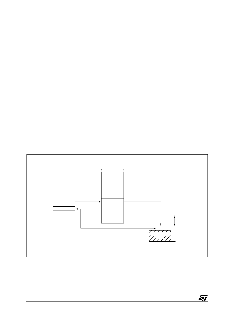
70/230
ST92163 - ON-CHIP DIRECT MEMORY ACCESS (DMA)
4 ON-CHIP DIRECT MEMORY ACCESS (DMA)
4.1 INTRODUCTION
The ST9 includes on-chip Direct Memory Access
(DMA) in order to provide high-speed data transfer
between peripherals and memory or Register File.
Multi-channel DMA is fully supported by peripher-
als having their own controller and DMA chan-
nel(s). Each DMA channel transfers data to or
from contiguous locations in the Register File, or in
Memory. The maximum number of bytes that can
be transferred per transaction by each DMA chan-
nel is 222 with the Register File, or 65536 with
Memory.
The DMA controller in the Peripheral uses an indi-
rect addressing mechanism to DMA Pointers and
Counter Registers stored in the Register File. This
is the reason why the maximum number of trans-
actions for the Register File is 222, since two Reg-
isters are allocated for the Pointer and Counter.
Register pairs are used for memory pointers and
counters in order to offer the full 65536 byte and
count capability.
4.2 DMA PRIORITY LEVELS
The 8 priority levels used for interrupts are also
used to prioritize the DMA requests, which are ar-
bitrated in the same arbitration phase as interrupt
requests. If the event occurrence requires a DMA
transaction, this will take place at the end of the
current instruction execution. When an interrupt
and a DMA request occur simultaneously, on the
same priority level, the DMA request is serviced
before the interrupt.
An interrupt priority request must be strictly higher
than the CPL value in order to be acknowledged,
whereas, for a DMA transaction request, it must be
equal to or higher than the CPL value in order to
be executed. Thus only DMA transaction requests
can be acknowledged when the CPL=0.
DMA requests do not modify the CPL value, since
the DMA transaction is not interruptable.
Figure 31. DMA Data Transfer
PERIPHERAL
VR001834
DATA
ADDRESS
COUNTER
TRANSFERRED
REGISTER FILE
OR
MEMORY
REGISTER FILE
REGISTER FILE
START ADDRESS
COUNTER VALUE
0
DF
DATA
GROUP F
PERIPHERAL
PAGED
REGISTERS
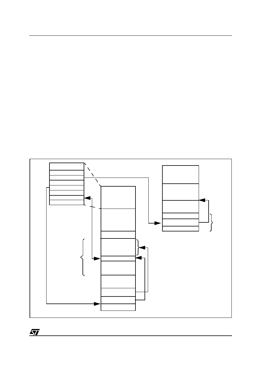
71/230
ST92163 - ON-CHIP DIRECT MEMORY ACCESS (DMA)
4.3 DMA TRANSACTIONS
The purpose of an on-chip DMA channel is to
transfer a block of data between a peripheral and
the Register File, or Memory. Each DMA transfer
consists of three operations:
≠ A load from/to the peripheral data register to/
from a location of Register File (or Memory) ad-
dressed through the DMA Address Register (or
Register pair)
≠ A post-increment of the DMA Address Register
(or Register pair)
≠ A post-decrement of the DMA transaction coun-
ter, which contains the number of transactions
that have still to be performed.
If the DMA transaction is carried out between the
peripheral and the Register File (
Figure 32
), one
register is required to hold the DMA Address, and
one to hold the DMA transaction counter. These
two registers must be located in the Register File:
the DMA Address Register in the even address
register, and the DMA Transaction Counter in the
next register (odd address). They are pointed to by
the DMA Transaction Counter Pointer Register
(DCPR), located in the peripheral's paged regis-
ters. In order to select a DMA transaction with the
Register File, the control bit DCPR.RM (bit 0 of
DCPR) must be set.
If the transaction is made between the peripheral
and Memory, a register pair (16 bits) is required
for the DMA Address and the DMA Transaction
Counter (
Figure 33
). Thus, two register pairs must
be located in the Register File.
The DMA Transaction Counter is pointed to by the
DMA Transaction Counter Pointer Register
(DCPR), the DMA Address is pointed to by the
DMA Address Pointer Register (DAPR),both
DCPR and DAPR are located in the paged regis-
ters of the peripheral.
Figure 32. DMA Between Register File and Peripheral
IDCR
IVR
DAPR
DCPR
DATA
PAGED
REGISTERS
REGISTERS
SYSTEM
DMA
COUNTER
DMA
ADDRESS
FFh
F0h
E0h
DFh
EFh
MEMORY
000000h
DATA
ALREADY
TRANSFERRED
END OF BLOCK
INTERRUPT
SERVICE ROUTINE
DMA
TABLE
DM
A TR
ANSA
CTIO
N
ISR ADDRESS
000100h
VECTOR
TABLE
REGISTER FILE
PERIPHERAL
PAGED REGISTERS
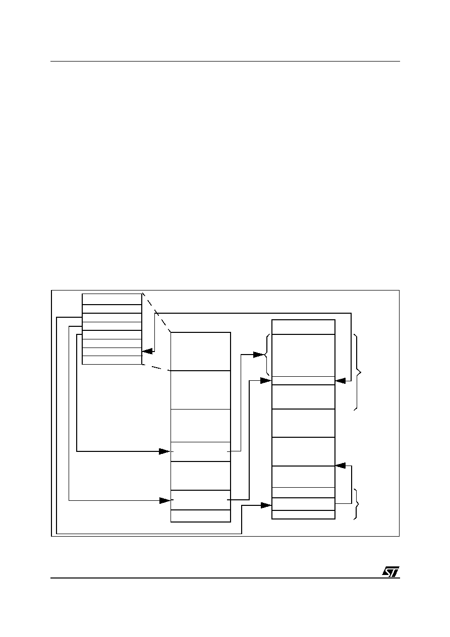
72/230
ST92163 - ON-CHIP DIRECT MEMORY ACCESS (DMA)
DMA TRANSACTIONS (Cont'd)
When selecting the DMA transaction with memory,
bit DCPR.RM (bit 0 of DCPR) must be cleared.
To select between using the ISR or the DMASR reg-
ister to extend the address, (see Memory Manage-
ment Unit chapter), the control bit DAPR.PS (bit 0
of DAPR) must be cleared or set respectively.
The DMA transaction Counter must be initialized
with the number of transactions to perform and will
be decremented after each transaction. The DMA
Address must be initialized with the starting ad-
dress of the DMA table and is increased after each
transaction. These two registers must be located
between addresses 00h and DFh of the Register
File.
Once a DMA channel is initialized, a transfer can
start. The direction of the transfer is automatically
defined by the type of peripheral and programming
mode.
Once the DMA table is completed (the transaction
counter reaches 0 value), an Interrupt request to
the CPU is generated.
When the Interrupt Pending (IDCR.IP) bit is set by
a hardware event (or by software), and the DMA
Mask bit (IDCR.DM) is set, a DMA request is gen-
erated. If the Priority Level of the DMA source is
higher than, or equal to, the Current Priority Level
(CPL), the DMA transfer is executed at the end of
the current instruction. DMA transfers read/write
data from/to the location pointed to by the DMA
Address Register, the DMA Address register is in-
cremented and the Transaction Counter Register
is decremented. When the contents of the Trans-
action Counter are decremented to zero, the DMA
Mask bit (DM) is cleared and an interrupt request
is generated, according to the Interrupt Mask bit
(End of Block interrupt). This End-of-Block inter-
rupt request is taken into account, depending on
the PRL value.
WARNING. DMA requests are not acknowledged
if the top level interrupt service is in progress.
Figure 33. DMA Between Memory and Peripheral
n
IDCR
IVR
DAPR
DCPR
DATA
PAGED
REGISTERS
REGISTERS
SYSTEM
DMA
TRANSACTION
COUNTER
DMA
ADDRESS
FFh
F0h
E0h
DFh
EFh
MEMORY
000000h
DATA
ALREADY
TRANSFERRED
END OF BLOCK
INTERRUPT
SERVICE ROUTINE
DMA
TABLE
DMA TRANSACTION
ISR ADDRESS
000100h
VECTOR
TABLE
REGISTER FILE
PERIPHERAL
PAGED REGISTERS

73/230
ST92163 - ON-CHIP DIRECT MEMORY ACCESS (DMA)
DMA TRANSACTIONS (Cont'd)
4.4 DMA CYCLE TIME
The interrupt and DMA arbitration protocol func-
tions completely asynchronously from instruction
flow.
Requests are sampled every 5 CPUCLK cycles.
DMA transactions are executed if their priority al-
lows it.
A DMA transfer with the Register file requires 8
CPUCLK cycles.
A DMA transfer with memory requires 16 CPUCLK
cycles, plus any required wait states.
4.5 SWAP MODE
An extra feature which may be found on the DMA
channels of some peripherals (e.g. the MultiFunc-
tion Timer) is the Swap mode. This feature allows
transfer from two DMA tables alternatively. All the
DMA descriptors in the Register File are thus dou-
bled. Two DMA transaction counters and two DMA
address pointers allow the definition of two fully in-
dependent tables (they only have to belong to the
same space, Register File or Memory). The DMA
transaction is programmed to start on one of the
two tables (say table 0) and, at the end of the
block, the DMA controller automatically swaps to
the other table (table 1) by pointing to the other
DMA descriptors. In this case, the DMA mask (DM
bit) control bit is not cleared, but the End Of Block
interrupt request is generated to allow the optional
updating of the first data table (table 0).
Until the swap mode is disabled, the DMA control-
ler will continue to swap between DMA Table 0
and DMA Table 1.
n
74/230
ST92163 - ON-CHIP DIRECT MEMORY ACCESS (DMA)
4.6 DMA REGISTERS
As each peripheral DMA channel has its own spe-
cific control registers, the following register list
should be considered as a general example. The
names and register bit allocations shown here
may be different from those found in the peripheral
chapters.
DMA COUNTER POINTER REGISTER (DCPR)
Read/Write
Address set by Peripheral
Reset value: undefined
Bit 7:1 = C[7:1]:
DMA Transaction Counter Point-
er.
Software should write the pointer to the DMA
Transaction Counter in these bits.
Bit 0 = RM:
Register File/Memory Selector.
This bit is set and cleared by software.
0: DMA transactions are with memory (see also
DAPR.DP)
1: DMA transactions are with the Register File
GENERIC EXTERNAL PERIPHERAL INTER-
RUPT AND DMA CONTROL (IDCR)
Read/Write
Address set by Peripheral
Reset value: undefined
Bit 5 = IP:
Interrupt Pending
.
This bit is set by hardware when the Trigger Event
occurs. It is cleared by hardware when the request
is acknowledged. It can be set/cleared by software
in order to generate/cancel a pending request.
0: No interrupt pending
1: Interrupt pending
Bit 4 = DM:
DMA Request Mask
.
This bit is set and cleared by software. It is also
cleared when the transaction counter reaches
zero (unless SWAP mode is active).
0: No DMA request is generated when IP is set.
1: DMA request is generated when IP is set
Bit 3 = IM:
End of block
Interrupt Mask
.
This bit is set and cleared by software.
0: No End of block interrupt request is generated
when IP is set
1: End of Block interrupt is generated when IP is
set. DMA requests depend on the DM bit value
as shown in the table below.
Bit 2:0 = PRL[2:0]:
Source
Priority Level
.
These bits are set and cleared by software. Refer
to Section 4.2 for a description of priority levels.
DMA ADDRESS POINTER REGISTER (DAPR)
Read/Write
Address set by Peripheral
Reset value: undefined
Bit 7:1 = A[7:1]:
DMA Address Register(s) Pointer
Software should write the pointer to the DMA Ad-
dress Register(s) in these bits.
Bit 0 = PS:
Memory Segment Pointer Selector
:
This bit is set and cleared by software. It is only
meaningful if DCPR.RM=0.
0: The ISR register is used to extend the address
of data transferred by DMA (see MMU chapter).
1: The DMASR register is used to extend the ad-
dress of data transferred by DMA (see MMU
chapter).
7
0
C7
C6
C5
C4
C3
C2
C1
RM
7
0
IP
DM
IM
PRL2 PRL1 PRL0
DM IM Meaning
1
0
A DMA request generated without End of Block
interrupt when IP=1
1
1
A DMA request generated with End of Block in-
terrupt when IP=1
0
0
No End of block interrupt or DMA request is
generated when IP=1
0
1
An End of block Interrupt is generated without
associated DMA request (not used)
PRL2 PRL1 PRL0 Source Priority Level
0
0
0
0 Highest
0
0
1
1
0
1
0
2
0
1
1
3
1
0
0
4
1
0
1
5
1
1
0
6
1
1
1
7 Lowest
7
0
A7
A6
A5
A4
A3
A2
A1
PS
75/230
ST92163 - RESET AND CLOCK CONTROL UNIT (RCCU)
5 RESET AND CLOCK CONTROL UNIT (RCCU)
5.1 INTRODUCTION
The Reset and Clock Control Unit (RCCU) com-
prises two distinct sections:
≠ the Clock Control Unit, which generates and
manages the internal clock signals.
≠ the Reset/Stop Manager, which detects and
flags Hardware, Software and Watchdog gener-
ated resets.
Note: To use the ST92163 with USB interface, the
RCCU must be configured as shown in
Figure 35
.
The external oscillator frequency must be 8 MHz.
Other configurations must not be used.
On ST9 devices where the external Stop pin is
available, this circuit also detects and manages
the externally triggered Stop mode, during which
all oscillators are frozen in order to achieve the
lowest possible power consumption.
5.2 CLOCK CONTROL UNIT
The Clock Control Unit generates the internal
clocks for the CPU core (CPUCLK) and for the on-
chip peripherals (INTCLK). The Clock Control Unit
may be driven by an external crystal circuit, con-
nected to the OSCIN and OSCOUT pins, or by an
external pulse generator, connected to OSCIN
(see
Figure 42
and
Figure 44
). Another clock
source named CK_AF can be provided from the
internal RC oscillator.
5.2.1 Clock Control Unit Overview
As shown in
Figure 34
, a programmable divider
can divide the CLOCK1 input clock signal by two.
The resulting signal, CLOCK2, is the reference in-
put clock to the programmable Phase Locked
Loop frequency multiplier, which is capable of mul-
tiplying the clock frequency by a factor of 6, 8, 10
or 14; the multiplied clock is then divided by a pro-
grammable divider, by a factor of 1 to 7. By this
means, the ST9 can operate with cheaper, medi-
um frequency (3-5 MHz) crystals, while still provid-
ing a high frequency internal clock for maximum
system performance; the range of available multi-
plication and division factors allow a great number
of operating clock frequencies to be derived from a
single crystal frequency. The undivided PLL clock
is also available for special purposes (high-speed
peripheral).
For low power operation, especially in Wait for In-
terrupt mode, the Clock Multiplier unit may be
turned off, whereupon the output clock signal may
be programmed as CLOCK2 divided by 16. For
further power reduction, an internal RC oscillator
with a frequency of 85KHZ (+/- 40%) is available to
provide the CK_AF clock internally if the external
clock source is not used. During the execution of a
WFI in Low Power mode this clock is further divid-
ed by 16 to reduce power consumption (for the se-
lection of this signal refer to the description the
CK_AF clock source in the following sections).
The internal system clock, INTCLK, is routed to all
on-chip peripherals, as well as to the programma-
ble Clock Prescaler Unit which generates the clock
for the CPU core (CPUCLK).
The Clock Prescaler is programmable and can
slow the CPU clock by a factor of up to 8, allowing
the programmer to reduce CPU processing speed,
and thus power consumption, while maintaining a
high speed clock to the peripherals. This is partic-
ularly useful when little actual processing is being
done by the CPU and the peripherals are doing
most of the work.
Figure 34. Clock Control Unit Simplified Block Diagram
Quartz
1/16
1/2
oscillator
CLOCK2
CLOCK1
CK_AF
PLL
Clock Multiplier
CPU Clock
Prescaler
to
CPU Core
to
Peripherals
CPUCLK
INTCLK
Unit
/Divider
1/16
RC
oscillator
Internal
76/230
ST92163 - RESET AND CLOCK CONTROL UNIT (RCCU)
Figure 35. ST92163 Clock Distribution Diagram
8 MHz
PLL
1/16
x
/2
DIV2=0
1/2
Oscillator
MX1=0 MX0=1
CSU_CKSEL=1
6
XT_DIV16=1
0
1
0
1
0
1
RCCU
24 MHz INTCLK
CLOCK2
3-bit Prescaler
CPU
MFT
1/3
8-
bi
t
Pr
es
c
a
l
e
r
1
6
-b
it
Up
/
D
o
w
n
Co
u
n
t
e
r
1...256
(Max INTCLK/3)
USB INTERFACE
Baud Rate
Generator
1/N
N=2...(2
16
-1)
SCI
1
6
-
b
it
Do
wn
C
oun
t
e
r
1/4
WDG
CPUCLK
EMBEDDED MEMORY
RAM
EPROM/ROM/OTP
I
2
C
STD
FAST
1/N
1/N
N=4,6,8...258
N=6,9,12...387
Fscl
100 kHz
Fscl
400 kHz
Fscl > 100 kHz
1...8
A/D
8
-
b
i
t
P
r
e
sca
l
e
r
1...256
P6.2
Quartz
DX2=0 DX1=0 DX0=2
(TxINA/TxINB)
48 MHz
0
1
1/16
RC
oscillator
0
1
WFI and LPOWFI=1 and WFI_CKSEL = 1
CK_AF
and WFI_CKSEL=1
or CK_ST=1
and LPOWFI=1
WFI
Internal
P6.3
8 MHz XTOUT
77/230
ST92163 - RESET AND CLOCK CONTROL UNIT (RCCU)
5.3 CLOCK MANAGEMENT
The various programmable features and operating modes of the CCU are handled by four registers:
≠ MODER (Mode Register)
This is a System Register (R235, Group E).
The input clock divide-by-two and the CPU clock
prescaler factors are handled by this register.
≠ CLKCTL (Clock Control Register)
This is a Paged Register (R240, Page 55).
The low power modes and the interpretation of
the HALT instruction are handled by this register.
≠ CLK_FLAG (Clock Flag Register)
This is a Paged Register (R242, Page 55).
This register contains various status flags, as
well as control bits for clock selection.
≠ PLLCONF (PLL Configuration Register)
This is a Paged Register (R246, Page 55).
The PLL multiplication and division factors are
programmed in this register.
Figure 36. Clock Control Unit Programming
Quartz
PLL
1/16
x
1/2
DIV2
CKAF_SEL
1/N
oscillator
MX(1:0)
0
1
0
1
0
1
CKAF_ST
CSU_CKSEL
6/8/10/14
1
0
XT_DIV16
DX(2:0)
CLOCK2
CLOCK1
(MODER)
(CLK_FLAG)
(CLKCTL)
(PLLCONF)
(CLK_FLAG)
CK_AF
INTCLK
to
Peripherals
and
CPU Clock Prescaler
XTSTOP
(CLK_FLAG)
Wait for Interrupt and Low Power Modes:
LPOWFI (CLKCTL) selects Low Power operation automatically on entering WFI mode.
WFI_CKSEL (CLKCTL) selects the CK_AF clock automatically, if present, on entering WFI mode.
XTSTOP (CLK_FLAG) automatically stops the Xtal oscillator when the CK_AF clock is present and selected.
OUTPLL_2
(USB CLOCK)
1/16
Internal
WFI and LPOWFI=1 and WFI_CKSEL = 1
1
0
oscillator
RC
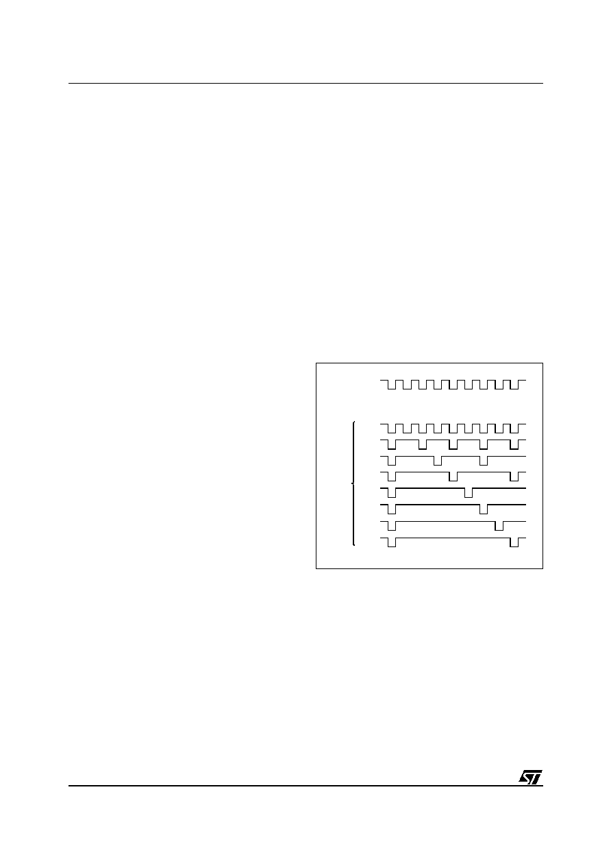
78/230
ST92163 - RESET AND CLOCK CONTROL UNIT (RCCU)
CLOCK MANAGEMENT (Cont'd)
5.3.1 PLL Clock Multiplier Programming
The CLOCK1 signal generated by the oscillator
drives a programmable divide-by-two circuit. If the
DIV2 control bit in MODER is set (Reset Condi-
tion), CLOCK2, is equal to CLOCK1 divided by
two; if DIV2 is reset, CLOCK2 is identical to
CLOCK1. A CLOCK1 signal with a semiperiod
(high or low) shorter than 40ns is forbidden if the
divider by two is disabled.
When the PLL is active, it multiplies CLOCK2 by 6,
8, 10 or 14, depending on the status of the MX0 -1
bits in PLLCONF. The multiplied clock is then di-
vided by a factor in the range 1 to 7, determined by
the status of the DX0-2 bits; when these bits are
programmed to 111, the PLL is switched off.
Following a RESET phase, programming bits
DX0-2 to a value different from 111 will turn the
PLL on. After allowing a stabilisation period for the
PLL, setting the CSU_CKSEL bit in the
CLK_FLAG Register selects the multiplier clock
This peripheral contains a lock-in logic that verifies
if the PLL is locked to the CLOCK2 frequency. The
bit LOCK in CLK_FLAG register becomes 1 when
this event occurs.
The maximum frequency allowed for INTCLK is
25MHz for 5V operation, and 12MHz for 3V opera-
tion. Care is required, when programming the PLL
multiplier and divider factors, not to exceed the
maximum permissible operating frequency for
INTCLK, according to supply voltage.
The ST9 being a static machine, there is no lower
limit for INTCLK. However, below 1MHz, A/D con-
verter precision (if present) decreases.
5.3.2 CPU Clock Prescaling
The system clock, INTCLK, which may be the out-
put of the PLL clock multiplier, CLOCK2, CLOCK2/
16 or CK_AF, drives a programmable prescaler
which generates the basic time base, CPUCLK,
for the instruction executer of the ST9 CPU core.
This allows the user to slow down program execu-
tion during non processor intensive routines, thus
reducing power dissipation.
The internal peripherals are not affected by the
CPUCLK prescaler and continue to operate at the
full INTCLK frequency. This is particularly useful
when little processing is being done and the pe-
ripherals are doing most of the work.
The prescaler divides the input clock by the value
programmed in the control bits PRS2,1,0 in the
MODER register. If the prescaler value is zero, no
prescaling takes place, thus CPUCLK has the
same period and phase as INTCLK. If the value is
different from 0, the prescaling is equal to the val-
ue plus one, ranging thus from two (PRS2,1,0 = 1)
to eight (PRS2,1,0 = 7).
The clock generated is shown in
Figure 37
, and it
will be noted that the prescaling of the clock does
not preserve the 50% duty cycle, since the high
level is stretched to replace the missing cycles.
This is analogous to the introduction of wait cycles
for access to external memory. When External
Memory Wait or Bus Request events occur, CPU-
CLK is stretched at the high level for the whole pe-
riod required by the function.
Figure 37. CPU Clock Prescaling
5.3.3 Peripheral Clock
The system clock, INTCLK, which may be the out-
put of the PLL clock multiplier, CLOCK2, CLOCK2/
16 or CK_AF, is also routed to all ST9 on-chip pe-
ripherals and acts as the central timebase for all
timing functions.
INTCLK
CPUCLK
VA00260
000
001
010
011
100
101
110
111
PRS VALUE
79/230
ST92163 - RESET AND CLOCK CONTROL UNIT (RCCU)
CLOCK MANAGEMENT (Cont'd)
5.3.4 Low Power Modes
The user can select an automatic slowdown of
clock frequency during Wait for Interrupt opera-
tion, thus idling in low power mode while waiting
for an interrupt. In WFI operation the clock to the
CPU core (CPUCLK) is stopped, thus suspending
program execution, while the clock to the peripher-
als (INTCLK) may be programmed as described in
the following paragraphs. An example of Low
Power operation in WFI is illustrated in
Figure 38
.
If low power operation during WFI is disabled
(LPOWFI bit = 0 in the CLKCTL Register), the
CPU CLK is stopped but INTCLK is unchanged.
If low power operation during Wait for Interrupt is
enabled (LPOWFI bit = 1 in the CLKCTL Register),
as soon as the CPU executes the WFI instruction,
the PLL is turned off and the system clock will be
forced to CLOCK2 divided by 16, or to CK_AF, if
this has been selected by setting WFI_CKSEL,
and providing CKAF_ST is set, thus indicating that
the internal RC oscillator is selected.
If the external clock source is used, the crystal os-
cillator may be stopped by setting the XTSTOP bit,
providing that the CK_AK clock is present and se-
lected, indicated by CKAF_ST being set. The crys-
tal oscillator will be stopped automatically on en-
tering WFI if the WFI_CKSEL bit has been set. It
should be noted that selecting a non-existent
CK_AF clock source is impossible, since such a
selection requires that the auxiliary clock source
be actually present and selected. In no event can
a non-existent clock source be selected inadvert-
ently.
It is up to the user program to switch back to a fast-
er clock on the occurrence of an interrupt, taking
care to respect the oscillator and PLL stabilisation
delays, as appropriate.It should be noted that any
of the low power modes may also be selected ex-
plicitly by the user program even when not in Wait
for Interrupt mode, by setting the appropriate bits.
5.3.5 Interrupt Generation
System clock selection modifies the CLKCTL and
CLK_FLAG registers.
The clock control unit generates an external inter-
rupt request when CK_AF and CLOCK2/16 are
selected or deselected as system clock source, as
well as when the system clock restarts after a
hardware stop (when the STOP MODE feature is
available on the specific device). This interrupt can
be masked by resetting the INT_SEL bit in the
CLKCTL register. In the RCCU the interrupt is
generated with a high to low transition (see inter-
rupt and DMA chapters for further information).
Table 13. Summary of Operating Modes using main Crystal Controlled Oscillator
MODE
INTCLK
CPUCLK
DIV2
PRS0-2
CSU_CKSEL
MX0-1 DX2-0
LPOWFI
XT_DIV16
PLL x BY 14
XTAL/2
x (14/D)
INTCLK/N
1
N-1
1
1 0
D-1
X
1
PLL x BY 10
XTAL/2
x (10/D)
INTCLK/N
1
N-1
1
0 0
D-1
X
1
PLL x BY 8
XTAL/2
x (8/D)
INTCLK/N
1
N-1
1
1 1
D-1
X
1
PLL x BY 6
XTAL/2
x (6/D)
INTCLK/N
1
N-1
1
0 1
D-1
X
1
SLOW 1
XTAL/2
INTCLK/N
1
N-1
X
X
111
X
1
SLOW 2
XTAL/32
INTCLK/N
1
N-1
X
X
X
X
0
WAIT FOR
INTERRUPT
If LPOWFI=0, no changes occur on INTCLK, but CPUCLK is stopped anyway.
LOW POWER
WAIT FOR
INTERRUPT
XTAL/32
STOP
1
X
X
X
X
1
1
RESET
XTAL/2
INTCLK
1
0
0
00
111
0
1
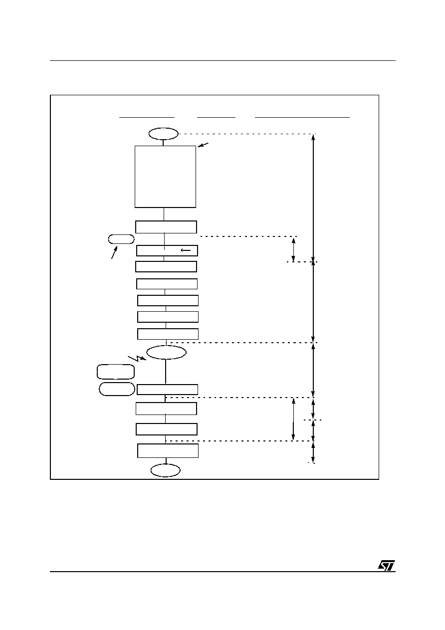
80/230
ST92163 - RESET AND CLOCK CONTROL UNIT (RCCU)
Figure 38. Example of Low Power Mode programming
Begin
WFI_CKSEL
1
WFI status
User's Program
LPOWFI
1
User's Program
WFI
End
PROGRAM FLOW
COMMENTS
SYSTEM CLOCK FREQUENCY
Interrupt
Quartz not divided by 2
PLL multiply factor
Multiplier divider's factor set
Wait for the
CK_AF clock selected when WFI
Wait For Interrupt
No code is executed until
Interrupt served
fixed to 6.
to 2, and PLL turned ON
an interrupt is requested
Low Power Mode enabled
Main code execution
continued
8 MHz
24 MHz
8 MHz
24 MHz
** T
2
= Quartz oscillator start-up time
* T
1
= PLL lock-in time
T
1
*
T
2
**
T
1
*
F
Q
=8 MHz, V
cc
=5 V and T=25∞C
RC
WAIT
DX2-0
001
Xtal is selected to
restart the PLL quickly
CSU_CKSEL
1
PLL is
system clock source
CSU_CKSEL<- 1
while the CK_AF is
the system clock
CKAF_SEL <- 0
The system CK
switches to Xtal
The PLL is locked
and becomes the
system clock
XTSTOP
0
To restart Xtal and PLL
To stop PLL and Xtal when
a WFI occurs
XTSTOP
1
PLL locking
SET UP AFTER RESET PHASE:
DIV2
=
0
XTSTOP = 0
MX(1:0)
=
01
CSU_CKSEL = 0
Interrupt
WAIT
Routine
(LOCK->1)
oscillator
RC
oscillator

81/230
ST92163 - RESET AND CLOCK CONTROL UNIT (RCCU)
5.4 CLOCK CONTROL REGISTERS
MODE REGISTER (MODER)
R235 - Read/Write
System Register
Reset Value: 1110 0000 (E0h)
*Note:
This register contains bits which relate to
other functions; these are described in the chapter
dealing with Device Architecture. Only those bits
relating to Clock functions are described here.
Bit 5 = DIV2:
OSCIN Divided by 2
.
This bit controls the divide by 2 circuit which oper-
ates on the OSCIN Clock.
0: No division of the OSCIN Clock
1: OSCIN clock is internally divided by 2
Bit 4:2 = PRS[2:0]:
Clock
Prescaling
.
These bits define the prescaler value used to pres-
cale CPUCLK from INTCLK. When these three
bits are reset, the CPUCLK is not prescaled, and is
equal to INTCLK; in all other cases, the internal
clock is prescaled by the value of these three bits
plus one.
CLOCK CONTROL REGISTER (CLKCTL)
R240 - Read Write
Register Page: 55
Reset Value: 0000 0000 (00h)
Bit 7 = INT_SEL:
Interrupt Selection
.
0: Select the external interrupt pin as interrupt
source (Reset state)
1: Select the internal RCCU interrupt (see
Section
5.3.5
)
Bit 6:4 = Reserved.
Must be kept reset for normal operation.
Bit 3 = SRESEN:
Software Reset Enable.
0: The HALT instruction turns off the quartz, the
PLL and the CCU
1: A Reset is generated when HALT is executed
Bit 2 = CKAF_SEL:
Alternate Function Clock Se-
lect.
0: CK_AF clock not selected
1: Select CK_AF clock
Note: To check if the selection has actually oc-
curred, check that CKAF_ST is set. If no CK_AF
clock is present, the selection will not occur.
Bit 1 = WFI_CKSEL:
WFI Clock Select
.
This bit selects the clock used in Low power WFI
mode if LPOWFI = 1.
0: INTCLK during WFI is CLOCK2/16
1: INTCLK during WFI is CK_AF, providing it is
present. In effect this bit sets CKAF_SEL in WFI
mode
WARNING: When the CK_AF is selected as Low
Power WFI clock but the XTAL is not turned off
(R242.4 = 0), after exiting from the WFI, CK_AF
will be still selected as system clock. In this case,
reset the R240.2 bit to switch back to the XT.
Bit 0 = LPOWFI:
Low Power mode during Wait For
Interrupt
.
0: Low Power mode during WFI disabled. When
WFI is executed, the CPUCLK is stopped and
INTCLK is unchanged
1: The ST9 enters Low Power mode when the WFI
instruction is executed. The clock during this
state depends on WFI_CKSEL
7
0
-
-
DIV2
PRS2
PRS1
PRS0
-
-
7
0
INT_S
EL
-
-
-
SRE-
SEN
CKAF_S
EL
WFI_CKS
EL
LPOW
FI

82/230
ST92163 - RESET AND CLOCK CONTROL UNIT (RCCU)
CLOCK CONTROL REGISTERS
CLOCK FLAG REGISTER (CLK_FLAG)
R242 -Read/Write
Register Page: 55
Reset Value: 0100 1000 after a Watchdog Reset
Reset Value: 0010 1000 after a Software Reset
Reset Value: 0000 1000 after a Power-On Reset
WARNING: If this register is accessed with a logi-
cal instruction, such as AND or OR, some bits may
not be set as expected.
WARNING: If you select the CK_AF as system
clock and turn off the oscillator (bits R240.2 and
R242.4 at 1), and then switch back to the XT clock
by resetting the R240.2 bit, you must wait for the
oscillator to restart correctly (12ms).
Bit 7 = EX_STP:
External Stop flag
This bit is set by hardware and cleared by soft-
ware.
0: No External Stop condition occurred
1: External Stop condition occurred
Bit 6 = WDGRES:
Watchdog reset flag.
This bit is read only.
0: No Watchdog reset occurred
1: Watchdog reset occurred
Bit 5 = SOFTRES:
Software Reset Flag.
This bit is read only.
0: No software reset occurred
1: Software reset occurred (HALT instruction)
Bit 4 = XTSTOP:
External Stop Enable.
0: External stop disabled
1: The Xtal oscillator will be stopped as soon as
the CK_AF clock is present and selected,
whether this is done explicitly by the user pro-
gram, or as a result of WFI, if WFI_CKSEL has
previously been set to select the CK_AF clock
during WFI.
WARNING: When the program writes `1' to the
XTSTOP bit, it will still be read as 0 and is only set
when the CK_AF clock is running (CKAF_ST=1).
Take care, as any operation such as a subsequent
AND with `1' or an OR with `0' to the XTSTOP bit
will reset it and the oscillator will not be stopped
even if CKAF_ST is subsequently set.
Bit 3 = XT_DIV16:
CLOCK/16 Selection
This bit is set and cleared by software. An interrupt
is generated when the bit is toggled.
0: CLOCK2/16 is selected and the PLL is off
1: The input is CLOCK2 (or the PLL output de-
pending on the value of CSU_CKSEL)
WARNING: After this bit is modified from 0 to 1,
take care that the PLL lock-in time has elapsed be-
fore setting the CSU_CKSEL bit.
Bit 2 = CKAF_ST: (Read Only)
If set, indicates that the alternate function clock
has been selected. If no CK_AF clock signal is
present on the pin, the selection will not occur. If
reset, the PLL clock, CLOCK2 or CLOCK2/16 is
selected (depending on bit 0).
Bit 1= LOCK:
PLL locked-in
This bit is read only.
0: The PLL is turned off or not locked and cannot
be selected as system clock source.
1: The PLL is locked
Bit 0 = CSU_CKSEL:
CSU Clock Select
This bit is set and cleared by software. It also
cleared by hardware when:
≠ bits DX[2:0] (PLLCONF) are set to 111;
≠ the quartz is stopped (by hardware or software);
≠ WFI is executed while the LPOWFI bit is set;
≠ the XT_DIV16 bit (CLK_FLAG) is forced to '0'.
This prevents the PLL, when not yet locked, from
providing an irregular clock. Furthermore, a `0'
stored in this bit speeds up the PLL's locking.
0: CLOCK2 provides the system clock
1: The PLL Multiplier provides the system clock.
NOTE: Setting the CKAF_SEL bit overrides any
other clock selection. Resetting the XT_DIV16 bit
overrides the CSU_CKSEL selection
7
0
EX_
STP
WDG
RES
SOFT
RES
XT-
STOP
XT_
DIV16
CKAF_
ST
LOC
K
CSU_
CK-
SEL
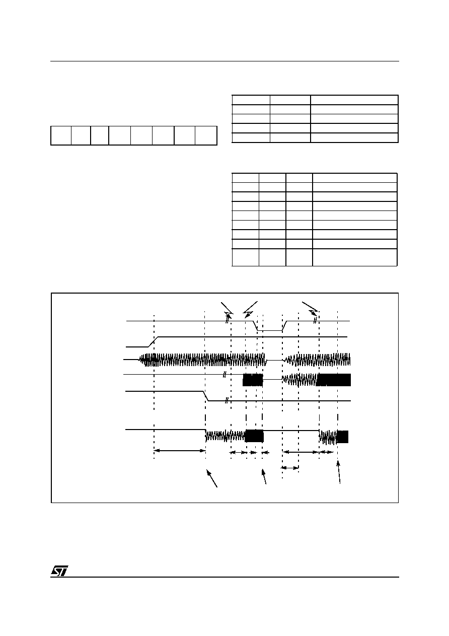
83/230
ST92163 - RESET AND CLOCK CONTROL UNIT (RCCU)
PLL CONFIGURATION REGISTER (PLLCONF)
R246 - Read/Write
Register Page: 55
Reset Value: xx00 x111
Bit 7:6 = Reserved.
Bit 5:4 = MX[1:0]:
PLL
Multiplication Factor
.
Refer to
Table 14
for multiplier settings.
Bit 3 = Reserved.
Bit 2:0 = DX[2:0]:
PLL output clock divider factor.
Refer to
Table 15
for divider settings.
Table 14. PLL Multiplication Factors
Table 15. Divider Configuration
Figure 39. RCCU General Timing
7
0
-
-
MX1
MX0
-
DX2
DX1
DX0
MX1
MX0
CLOCK2 x
1
0
14
0
0
10
1
1
8
0
1
6
DX2
DX1
DX0
CK
0
0
0
PLL CLOCK/1
0
0
1
PLL CLOCK/2
0
1
0
PLL CLOCK/3
0
1
1
PLL CLOCK/4
1
0
0
PLL CLOCK/5
1
0
1
PLL CLOCK/6
1
1
0
PLL CLOCK/7
1
1
1
CLOCK2
(PLL OFF, Reset State)
STOP
Acknowledged
STOP
External
Multiplier
Xtal
INTCLK
Internal
reset
clock
clock
RESET
pin
PLL selected by user
((N-1)*512+510)xT
Xtal
(**)
PLL
Lock-in
time
PLL
Lock-in
time
4 xT
sys
Quartz
start-up
Exit from RESET
510 x T
Xtal
(*)
(*) if DIV2 =1
Switch to
PLL clock
(**) +/- 1 T
Xtal
PLL turned on by user
Xtal/2
PLL
PLL
Xtal/2
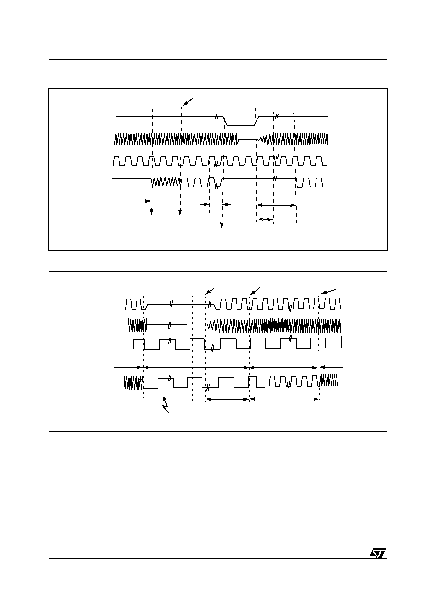
84/230
ST92163 - RESET AND CLOCK CONTROL UNIT (RCCU)
Figure 40. RCCU Timing during STOP (CK_AF System Clock)
Figure 41. Low Power Mode with a Stopped Quartz Oscillator
STOP
Xtal
clock
pin
((N-1)*512+510) x T
Xtal
(**)
4 xT
sys
Quartz
start-up
Exit from
STOP
510 x T
Xtal
(*)
Acknowledged
(*) if DIV2 =1
RC osc
clock
(**) +/- 1 T
Xtal
INTCLK
RESET
CK_AF
selected
CKAF_SEL<-1
INTCLK
WFI state
Multiplier
clock
Xtal
clock
Interrupt
Xtal restart time
PLL Lock-in time
T
sys
=2 xT
Xtal
PLL
l
With:
DIV2=1
RC osc
clock
(T
sys
= T
CK_AF
)
XTSTOP<-0
CSU_CKSEL<-1
CKAF_SEL<-0
PLL
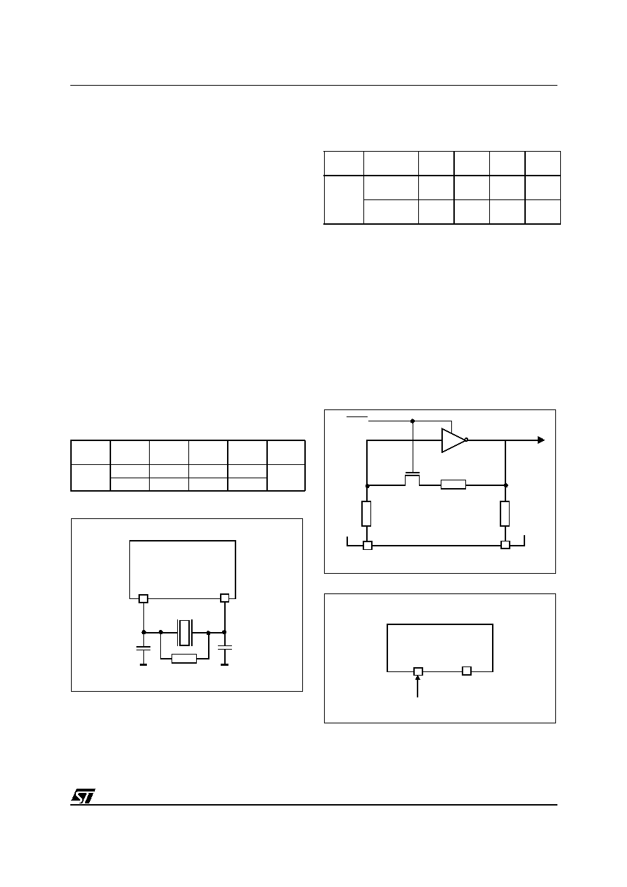
85/230
ST92163 - RESET AND CLOCK CONTROL UNIT (RCCU)
5.5 OSCILLATOR CHARACTERISTICS
The oscillator circuit uses an inverting gate circuit
with tri-state output.
Notes:
Owing to the Q factor required, Ceramic
Resonators may not provide a reliable oscillator
source
.
OSCOUT must not be directly used to drive exter-
nal circuits.
When the oscillator is stopped, OSCOUT goes
high impedance.
In Halt mode, set by means of the
HALT
instruc-
tion, the parallel resistor, R, is disconnected and
the oscillator is disabled, forcing the internal clock,
CLOCK1, to a high level, and OSCOUT to a high
impedance state.
To exit the
HALT
condition and restart the oscilla-
tor, an external RESET pulse is required.
It should be noted that, if the Watchdog function is
enabled, a
HALT
instruction will not disable the os-
cillator. This to avoid stopping the Watchdog if a
HALT
code is executed in error. When this occurs,
the CPU will be reset when the Watchdog times
out or when an external reset is applied.
Table 16. Oscillator Transconductance
Figure 42. Crystal Oscillator
Table 17. Crystal Internal Resistance
Legend:
C
1
, C
2
: Maximum Total Capacitances on pins OSCIN and
OSCOUT (the value includes the external capacitance
tied to the pin CL1 and CL2 plus the parasitic capacitance
of the board and of the device).
Rsmax: The equivalent serial resistor of the crystal.
Note 1: The tables are relative to the fundamental quartz
crystal only (not ceramic resonator).
Note 2: To reduce the parasitic capacitance, it is recom-
mended to place the crystal as close to the ST9 MCU as
possible.
WARNING: At low temperature, frost and humidity might
prevent the correct start-up of the oscillator.
Figure 43. Internal Oscillator Schematic
Figure 44. External Clock
Symbol
Voltage
range
Min
Typ
Max
Unit
gm
4.0-5.5V
0.77
1.5
2.4
mA/V
3.0-4.0V
0.5
0.73
1.47
OSCIN
OSCOUT
C
L1
C
L2
ST9
CRYSTAL CLOCK
VR02116A
1M*
*Recommended for oscillator stability
8 MHz
Symbol Conditions C
1
=C
2
= 56pF
C
1
=C
2
= 47pF
C
1
=C
2
= 33pF
C
1
=C
2
= 22pF
Rsmax
(ohm)
4.0-5.5V
Freq.=8MHz
50
65
120
180
3.0-4.0V
Freq.=8MHz
30
40
70
110
VR02086A
HALT
OSCIN
OSCOUT
R
IN
R
OUT
R
CLOCK1
OSCIN
OSCOUT
CLOCK
INPUT
NC
EXTERNAL CLOCK
VR02116B
ST9
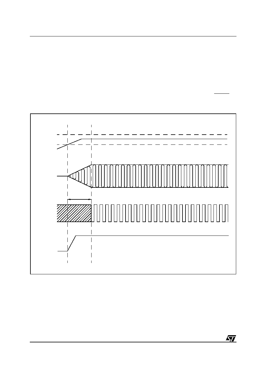
86/230
ST92163 - RESET AND CLOCK CONTROL UNIT (RCCU)
5.6 RESET/STOP MANAGER
The Reset/Stop Manager resets the MCU when
one of the three following events occurs:
≠ A Hardware reset, initiated by a low level on the
Reset pin.
≠ A Software reset, initiated by a HALT instruction
(when enabled).
≠ A Watchdog end of count condition.
The event which caused the last Reset is flagged
in the CLK_FLAG register, by setting the SOF-
TRES or the WDGRES bits respectively; a hard-
ware initiated reset will leave both these bits reset.
The hardware reset overrides all other conditions
and forces the ST9 to the reset state. During Re-
set, the internal registers are set to their reset val-
ues, where these are defined, and the I/O pins are
set to the Bidirectional Weak Pull-up mode.
Reset is asynchronous: as soon as the RESET pin
is driven low, a Reset cycle is initiated.
Figure 45. Oscillator Start-up Sequence and Reset Timing
V
DD
MAX
V
DD
MIN
OSCIN
INTCLK
RESET
OSCOUT
PIN
10ms
VR02085A
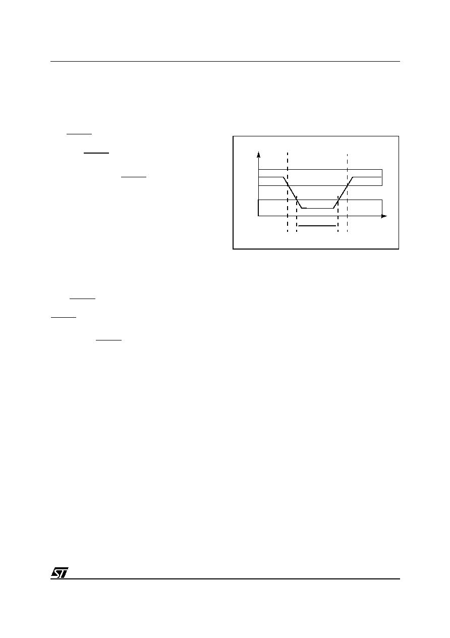
87/230
ST92163 - RESET AND CLOCK CONTROL UNIT (RCCU)
RESET/STOP MANAGER (Cont'd)
The on-chip Timer/Watchdog generates a reset
condition if the Watchdog mode is enabled
(WCR.WDEN cleared, R252 page 0), and if the
programmed period elapses without the specific
code (AAh, 55h) written to the appropriate register.
The RESET input pin is not driven low by the on-
chip reset generated by the Timer/Watchdog.
When the RESET pin goes high again, a delay of 10
ms occurs before exiting the Reset state (+-1
CLOCK1 period, depending on the delay between
the rising edge of the RESET pin and the first rising
edge of CLOCK1).
Subsequently a short Boot rou-
tine is executed from the device internal Boot ROM,
and control then passes to the user program.
The Boot routine sets the device characteristics
and loads the correct values in the Memory Man-
agement Unit's pointer registers, so that these
point to the physical memory areas as mapped in
the specific device. The precise duration of this
short Boot routine varies from device to device,
depending on the Boot ROM contents.
At the end of the Boot routine the Program Coun-
ter will be set to the location specified in the Reset
Vector located in the lowest two bytes of memory.
5.6.1 RESET Pin Timing
To improve the noise immunity of the device, the
RESET pin has a Schmitt trigger input circuit with
hysteresis. In addition, a filter will prevent an un-
wanted reset in case of a single glitch of less than
50 ns on the RESET pin. The device is certain to
reset if a negative pulse of more than 20µs is ap-
plied. When the reset pin goes high again, a delay
of up to 4µs (at 8 MHz.) will elapse before the
RCCU detects this rising front. From this event on,
79870 (about 10 ms at 8 MHz.) oscillator clock cy-
cles (CLOCK1) are counted before exiting the Re-
set state (+-1 CLOCK1 period depending on the
delay between the positive edge the RCCU de-
tects and the first rising edge of CLOCK1)
Figure 46. Recommended Signal to be Applied
on Reset Pin
5.7 STOP MODE
In Stop mode, the Reset/Stop Manager can also
stop all oscillators without resetting the device.
For information on entering and exiting Stop
Mode, refer to the Wake-Up/Interrupt lines man-
agement unit (WUIMU) chapter. In Stop Mode, all
context information is preserved and the internal
clock is frozen in the high state.
On exiting Stop mode, the MCU resumes execu-
tion of the user program after a delay of 255
CLOCK2 periods, an interrupt is generated and
the EX_STP bit in CLK_FLAG is set.
V
RESET
V
CC
0.7 V
CC
0.3 V
CC
20 µs
Minimum
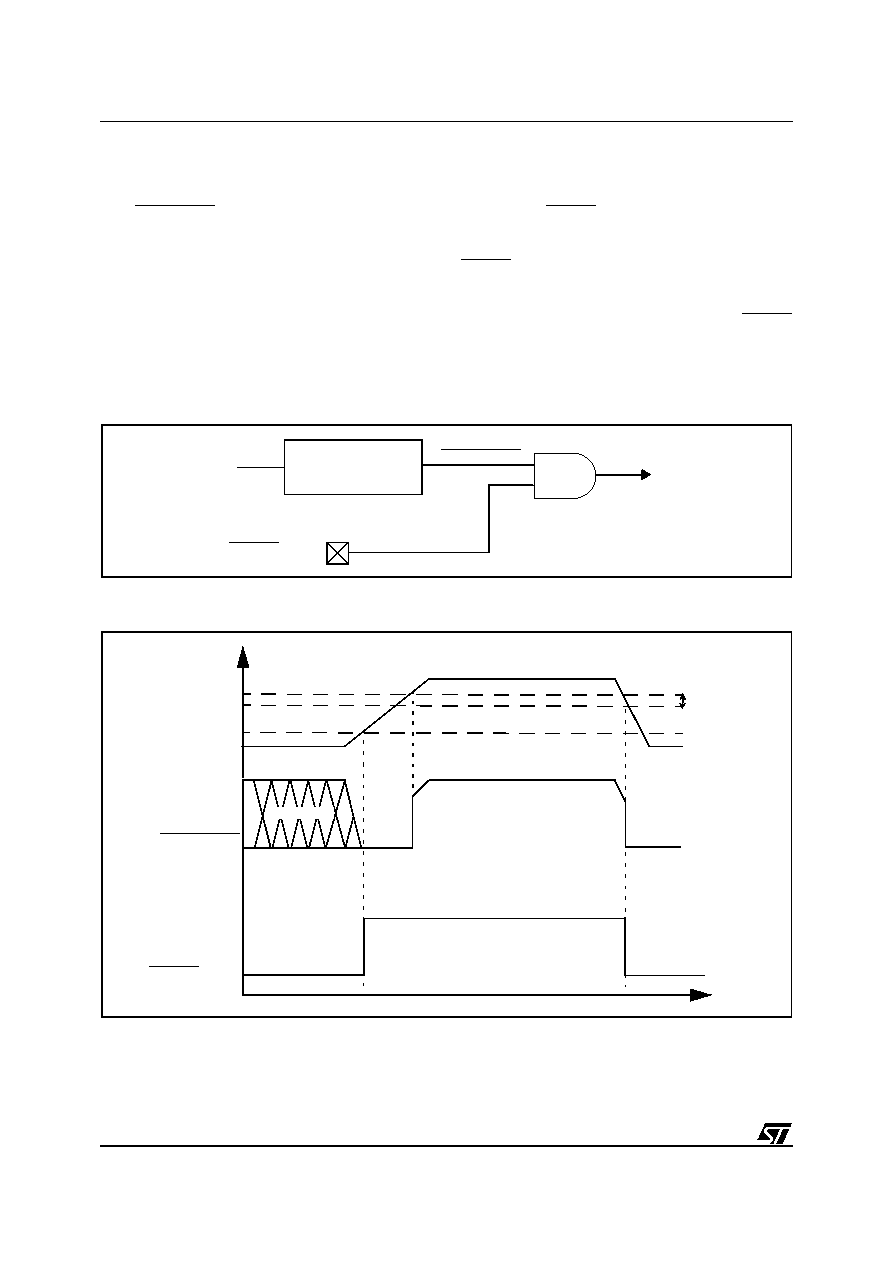
88/230
ST92163 - RESET AND CLOCK CONTROL UNIT (RCCU)
5.8 LOW VOLTAGE DETECTOR (LVD) RESET
The on-chip Low Voltage Detector (LVD) gener-
ates LVDRESET when the supply voltage drops
below a reference value (brown-out protection).
The reference value for the voltage drop is lower
than the reference value for power-up in order to
avoid a parasitic reset when the MCU starts run-
ning and sinks current on the supply (hysteresis).
The LVD circuitry generates a reset when V
DD
is:
≠ Above V
LVDMIN
and below V
IT+
when V
DD
is
rising
≠ Above V
LVDMIN
and below V
IT-
when V
DD
is
falling
Note: At power on, application must ensure that
the external RESET pin is held low until the V
DD
power supply reaches V
LVDMIN
.
Additionally, if V
DD
drops below V
LVDMIN
, a
RESET signal must be generated externally to re-
start the microcontroller.
The Low Voltage Detector circuitry resets only the
MCU and it does not change the external RESET
pin status: no reset signal for an external applica-
tion is generated.
Figure 47. Low Voltage Detector Reset Function
Figure 48. Low Voltage Detector Reset Signal
Note: Refer to the Electrical Characteristics section for the values of V
DD
, V
LVDMIN ,
V
IT+,
V
IT-
and V
HYS
.
Low Voltage
Detector
V
DD
RESET
Internal Reset
(External pin)
LVDRESET
LVDRESET
V
LVDMIN
V
IT+
V
IT-
V
DD
RESET (Ext.)
V
HYS
t
V
Undefined
89/230
ST92163 - RESET AND CLOCK CONTROL UNIT (RCCU)
LOW VOLTAGE DETECTOR (LVD) RESET (Cont'd)
Figure 49
gives an example of an external Power
On Reset circuit for power supplies with very slow
power on ramp.
This circuitry is composed of 1 PNP transistor, 2
resistors and 1 capacitor. It is thus cheaper than
an integrated P.O.R.
For more details, refer to Application note AN1366
Figure 49. Suggested External POR Circuit for applications with very slow V
DD
ramp up
Figure 50. External Connection for RESET pin for applications with fast V
DD
ramp up
RESET
ST92163
C1
V
DD
R1
R2
T1
R1 = 270 Kohms, +/- 2 %
R1 = 1 Mohms, +/- 2 %
C1 = 1 µF, accuracy not important
T1 = BC857, PNP transistor with:
h
fe
gain about 100
V
eb
= 0.55 v , min = 0.5 v, max = 0.6 v
RESET
ST92163
1
µ
F
V
DD
10k
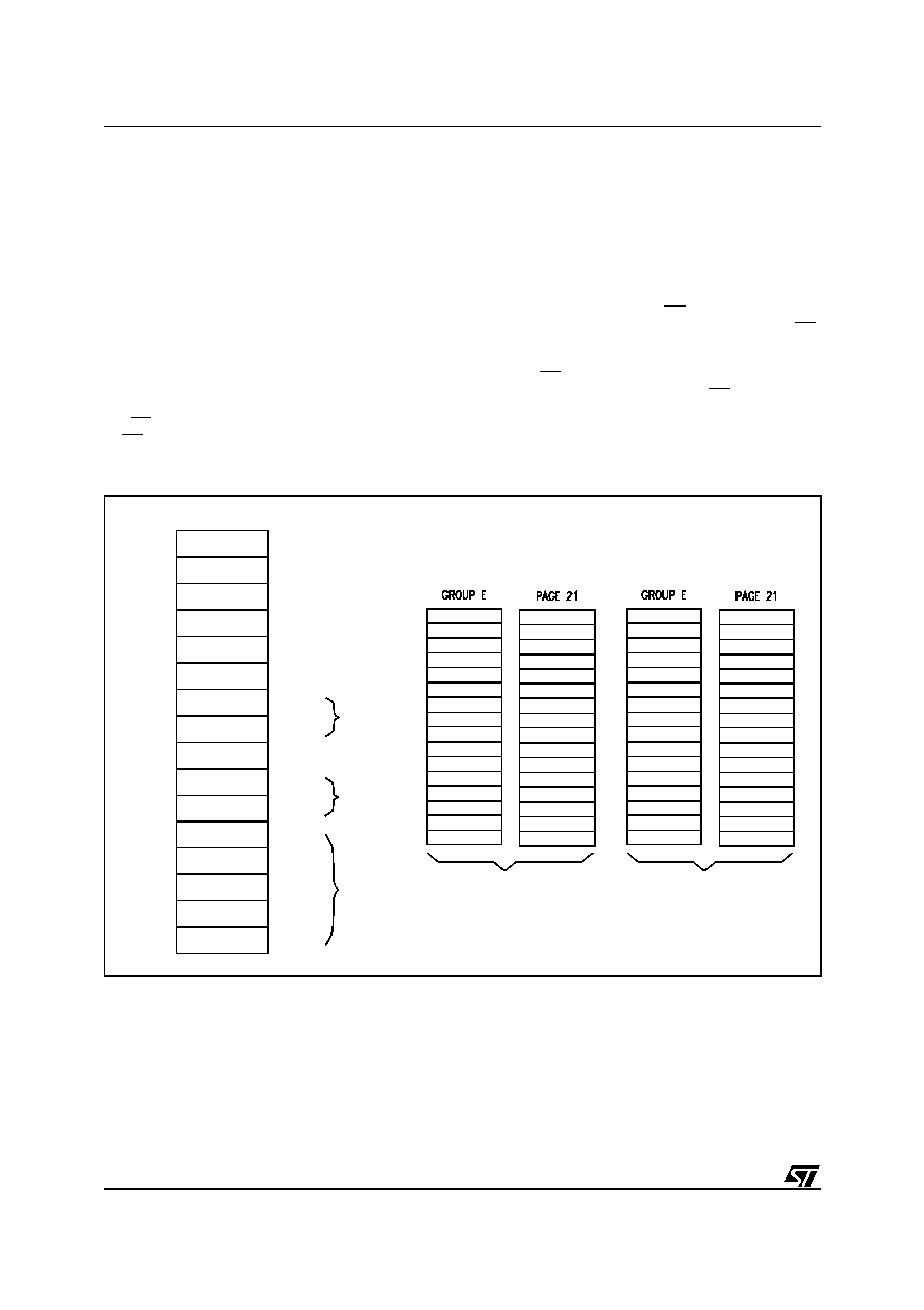
90/230
ST92163 - EXTERNAL MEMORY INTERFACE (EXTMI)
6 EXTERNAL MEMORY INTERFACE (EXTMI)
6.1 INTRODUCTION
The ST9 External Memory Interface uses two reg-
isters (EMR1 and EMR2) to configure external
memory accesses. Some interface signals are
also affected by WCR - R252 Page 0.
If the two registers EMR1 and EMR2 are set to the
proper values, the memory access cycle is similar
to that of the original ST9, with the only exception
that it is composed of just two system clock phas-
es, named T1 and T2.
During phase T1, the memory address is output on
the AS falling edge and is valid on the rising edge
of AS. Port0 and Port 1 maintain the address sta-
ble until the following T1 phase.
During phase T2, two forms of behavior are possi-
ble. If the memory access is a Read cycle, Port 0
pins are released in high-impedance until the next
T1 phase and the data signals are sampled by the
ST9 on the rising edge of DS. If the memory ac-
cess is a Write cycle, on the falling edge of DS,
Port 0 outputs data to be written in the external
memory. Those data signals are valid on the rising
edge of DS and are maintained stable until the
next address is output. Note that DS is pulled low
at the beginning of phase T2 only during an exter-
nal memory access.
Figure 51. Page 21 Registers
n
DMASR
ISR
EMR2
EMR1
CSR
DPR3
DPR2
DPR1
DPR0
R255
R254
R253
R252
R251
R250
R249
R248
R247
R246
R245
R244
R243
R242
R241
R240
FFh
FEh
FDh
FCh
FBh
FAh
F9h
F8h
F7h
F6h
F5h
F4h
F3h
F2h
F1h
F0h
MMU
EXT.MEM
Page 21
MMU
Bit DPRREM=0
SSPL
SSPH
USPL
USPH
MODER
PPR
RP1
RP0
FLAGR
CICR
P5
P4
P3
P2
P1
P0
DMASR
ISR
EMR2
EMR1
CSR
DPR3
DPR2
DPR1
DPR0
Bit DPRREM=1
SSPL
SSPH
USPL
USPH
MODER
PPR
RP1
RP0
FLAGR
CICR
P5
P4
P3
P2
P1
P0
DMASR
ISR
EMR2
EMR1
CSR
DPR3
DPR2
DPR1
DPR0
Relocation of P[3:0] and DPR[3:0] Registers

91/230
ST92163 - EXTERNAL MEMORY INTERFACE (EXTMI)
6.2 EXTERNAL MEMORY SIGNALS
The access to external memory is made using at
least AS, DS, Port 0 and Port 1. RW, DS2, BREQ,
BACK and WAIT signals improve functionality but
are not always present on ST9 devices.
Refer to
Figure 52
6.2.1 AS: Address Strobe
AS (Output, Active low, Tristate) is active during
the System Clock high-level phase of each T1
memory cycle: an AS rising edge indicates that
Memory Address and Read/Write Memory control
signals are valid. AS is released in high-imped-
ance during the bus acknowledge cycle or under
the processor control by setting the HIMP bit
(MODER.0, R235). Depending on the device AS is
available as Alternate Function or as a dedicated
pin.
Under Reset, AS is held high with an internal weak
pull-up.
The behavior of this signal is affected by the MC,
ASAF, ETO, BSZ, LAS[1:0] and UAS[1:0] bits in
the EMR1 or EMR2 registers. Refer to the Regis-
ter description.
6.2.2 DS: Data Strobe
DS (Output, Active low, Tristate) is active during the
internal clock high-level phase of each T2 memory
cycle. During an external memory read cycle, the
data on Port 0 must be valid before the DS rising
edge. During an external memory write cycle, the
data on Port 0 are output on the falling edge of DS
and they are valid on the rising edge of DS. When
the internal memory is accessed DS is kept high
during the whole memory cycle. DS is released in
high-impedance during bus acknowledge cycle or
under processor control by setting the HIMP bit
(MODER.0, R235). Under Reset status, DS is held
high with an internal weak pull-up.
The behavior of this signal is affected by the MC,
DS2EN, and BSZ bits in the EMR1 register. Refer
to the Register description.
6.2.3 DS2: Data Strobe 2
This additional Data Strobe pin (Alternate Function
Output, Active low, Tristate) is available on some
ST9 devices only. It allows two external memories
to be connected to the ST9, the upper memory
block (A21=1 typically RAM) and the lower memo-
ry block (A21=0 typically ROM) without any exter-
nal logic. The selection between the upper and
lower memory blocks depends on the A21 address
pin value.
The upper memory block is controlled by the DS
pin while the lower memory block is controlled by
the DS2 pin. When the internal memory is ad-
dressed, DS2 is kept high during the whole mem-
ory cycle. DS2 is released in high-impedance dur-
ing bus acknowledge cycle or under processor
control by setting the HIMP bit (MODER.0, R235).
DS2 is enabled via software as the Alternate Func-
tion output of the associated I/O port bit (refer to
specific ST9 version to identify the specific port
and pin).
The behavior of this signal is affected by the
DS2EN, and BSZ bits in the EMR1 register. Refer
to the Register description.
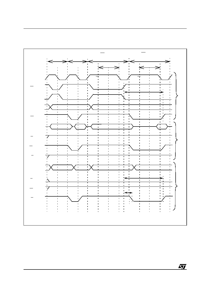
92/230
ST92163 - EXTERNAL MEMORY INTERFACE (EXTMI)
EXTERNAL MEMORY SIGNALS (Cont'd)
Figure 52. External memory Read/Write with and without a programmable wait
n
n
n
n
AS STRETCH
DS STRETCH
ADDRESS
ADDRESS
ADDRESS
ADDRESS
DATA IN
DATA IN
DATA OUT
DATA
T1
T2
T1
T2
TWA
TWD
NO WAIT CYCLE
1 AS WAIT CYCLE
1 DS WAIT CYCLE
ALW
AYS
RE
AD
W
RITE
AS (MC=0)
ALE (MC=1)
P1
DS (MC=0)
P0
MULTIPLEXED
RW (MC=0)
DS (MC=1)
RW (MC=1)
P0
MULTIPLEXED
RW (MC=0)
DS (MC=1)
RW (MC=1)
ADDRESS
ADDRESS
TAVQV
TAVWH
TAVWL
SYSTEM
CLOCK
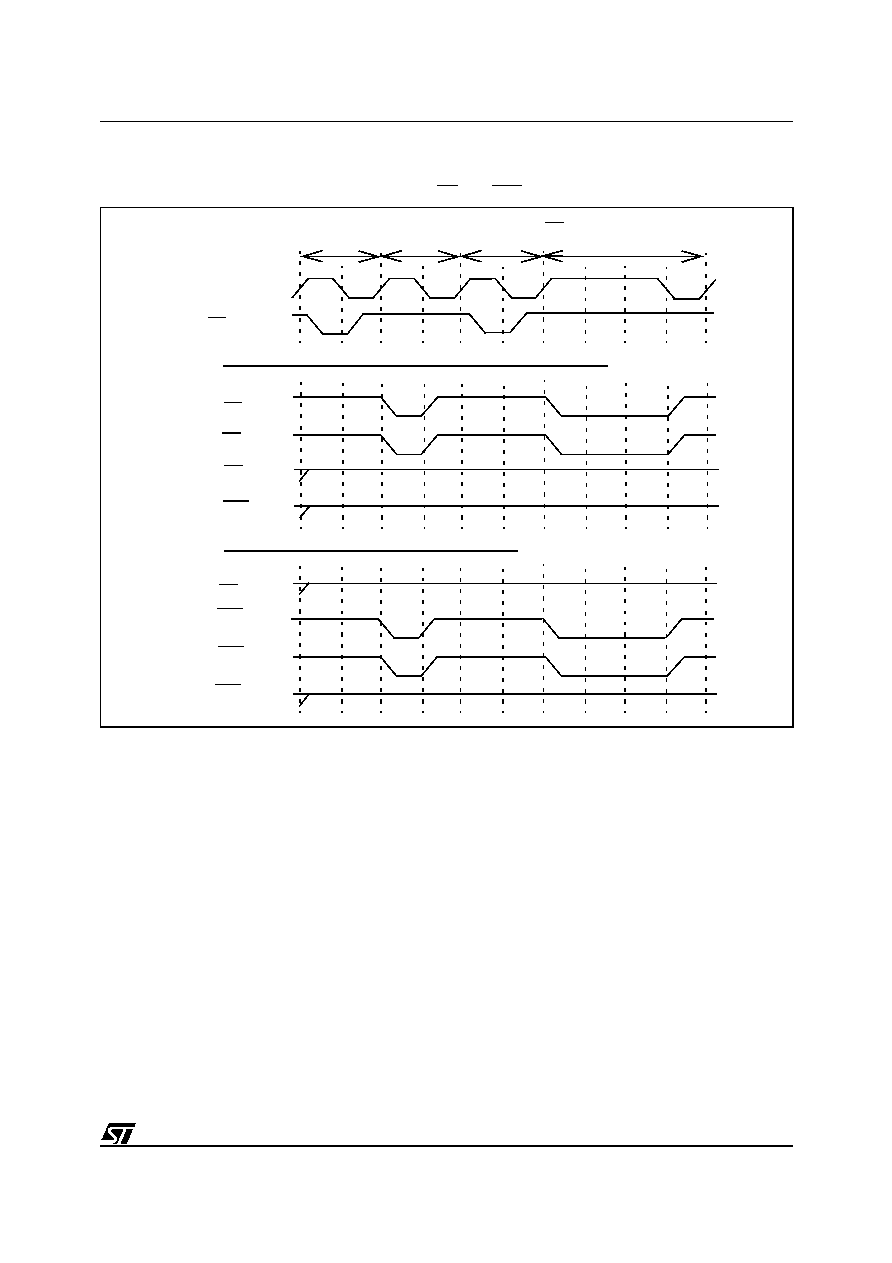
93/230
ST92163 - EXTERNAL MEMORY INTERFACE (EXTMI)
EXTERNAL MEMORY SIGNALS (Cont'd)
Figure 53. Effects of DS2EN on the behavior of DS and DS2
n
n
DS STRETCH
T1
T2
T1
T2
NO WAIT CYCLE
1 DS WAIT CYCLE
SYSTEM
AS (MC=0)
DS2EN=0 OR (DS2EN=1 AND UPPER MEMORY ADDRESSED):
DS2EN=1 AND LOWER MEMORY ADDRESSED:
DS
DS
DS
DS2
(MC=1, READ)
(MC=1, WRITE)
(MC=0)
DS
DS2
(MC=0)
DS2
(MC=1, READ)
DS2
(MC=1, WRITE)
CLOCK
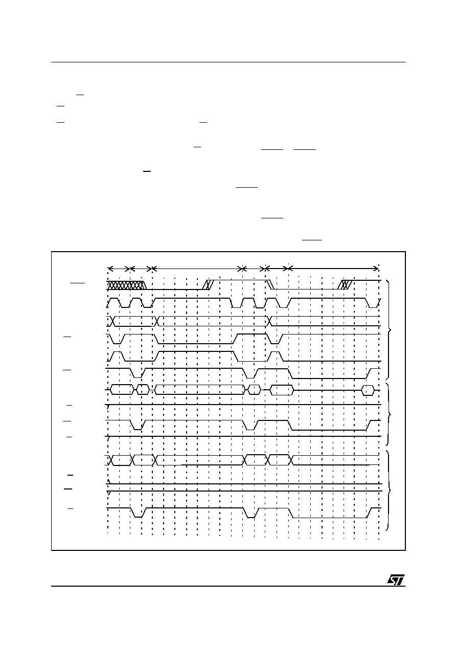
94/230
ST92163 - EXTERNAL MEMORY INTERFACE (EXTMI)
EXTERNAL MEMORY SIGNALS (Cont'd)
6.2.4 RW: Read/Write
RW (Alternate Function Output, Active low,
Tristate) identifies the type of memory cycle:
RW="1" identifies a memory read cycle, RW="0"
identifies a memory write cycle. It is defined at the
beginning of each memory cycle and it remains
stable until the following memory cycle. RW is re-
leased in high-impedance during bus acknowl-
edge cycle or under processor control by setting
the HIMP bit (MODER). RW is enabled via soft-
ware as the Alternate Function output of the asso-
ciated I/O port bit (refer to specific ST9 device to
identify the port and pin). Under Reset status, the
associated bit of the port is set into bidirectional
weak pull-up mode.
Note: On some devices, the internal weak pull-up
is not present. In this case, an external one is
needed.
The behavior of this signal is affected by the MC,
ETO and BSZ bits in the EMR1 register. Refer to
the Register description.
6.2.5 BREQ, BACK: Bus Request, Bus
Acknowledge
Note: These pins are available only on some ST9
devices (see Pin description).
BREQ (Alternate Function Input, Active low) indi-
cates to the ST9 that a bus request has tried or is
trying to gain control of the memory bus. Once en-
abled by setting the BRQEN bit (MODER.1,
R235), BREQ is sampled with the falling edge of
the processor internal clock during phase T2.
n
n
Figure 54. External memory Read/Write sequence with external wait (WAIT pin)
n
T1
T2
T1
T2
ALW
AYS
READ
WR
ITE
SYSTEM
AS (MC=0)
ALE (MC=1)
DS (MC=0)
P0
MULTIPLEXED
RW (MC=0)
DS (MC=1)
RW (MC=1)
P0
MULTIPLEXED
RW (MC=0)
DS (MC=1)
RW (MC=1)
WAIT
P1
T1
T2
ADDRESS
ADD.
ADD.
ADD.
D.OUT
ADDRESS
D.OUT
ADD.
DATA OUT
D.IN
D.IN
D.IN
ADDRESS
ADDRESS
ADDRESS
CLOCK
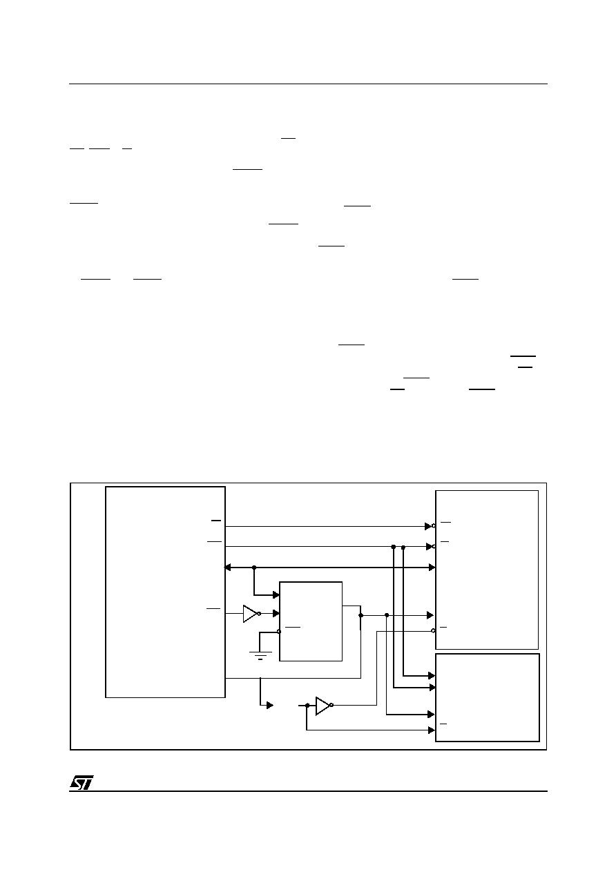
95/230
ST92163 - EXTERNAL MEMORY INTERFACE (EXTMI)
EXTERNAL MEMORY SIGNALS (Cont'd)
Whenever it is sampled low, the System Clock is
stretched and the external memory signals (AS,
DS, DS2, RW, P0 and P1) are released in high-im-
pedance. The external memory interface pins are
driven again by the ST9 as soon as BREQ is sam-
pled high.
BACK (Alternate Function Output, Active low) indi-
cates that the ST9 has relinquished control of the
memory bus in response to a bus request. BREQ
is driven low when the external memory interface
signals are released in high-impedance.
At MCU reset, the bus request function is disabled.
To enable it, configure the I/O port pins assigned
to BREQ and BACK as Alternate Function and set
the BRQEN bit in the MODER register.
6.2.6 PORT 0
If Port 0 (Input/Output, Push-Pull/Open-Drain/
Weak Pull-up) is used as a bit programmable par-
allel I/O port, it has the same features as a regular
port. When set as an Alternate Function, it is used
as the External Memory interface: it outputs the
multiplexed Address 8 LSB: A[7:0] /Data bus
D[7:0].
6.2.7 PORT 1
If Port 1 (Input/Output, Push-Pull/Open-Drain/
Weak Pull-up) is used as a bit programmable par-
allel I/O port, it has the same features as a regular
port. When set as an Alternate Function, it is used
as the external memory interface to provide the 8
MSB of the address A[15:8].
The behavior of the Port 0 and 1 pins is affected by
the BSZ and ETO bits in the EMR1 register. Refer
to the Register description.
6.2.8 WAIT: External Memory Wait
Note: This pin is available only on some ST9 de-
vices (see Pin description).
WAIT (Alternate Function Input, Active low) indi-
cates to the ST9 that the external memory requires
more time to complete the memory access cycle. If
bit EWEN (EIVR) is set, the WAIT signal is sam-
pled with the rising edge of the processor internal
clock during phase T1 or T2 of every memory cy-
cle. If the signal was sampled active, one more in-
ternal clock cycle is added to the memory cycle.
On the rising edge of the added internal clock cy-
cle, WAIT is sampled again to continue or finish
the memory cycle stretching. Note that if WAIT is
sampled active during phase T1 then AS is
stretched, while if WAIT is sampled active during
phase T2 then DS is stretched. WAIT is enabled
via software as the Alternate Function input of the
associated I/O port bit (refer to specific ST9 ver-
sion to identify the specific port and pin). Under
Reset status, the associated bit of the port is set to
the bidirectional weak pull-up mode. Refer to
Fig-
ure 54
Figure 55. Application Example
RAM
32 Kbytes
G
E
A0-A14
A[8:15]
ST9
DS
P1
Q0-Q7
P0
W
RW
D[8:1]
AS
OE
LE
Q[8:1]
A[7:0]/D[7:0]
LATCH
A15
DS
DATA Q[7:0]
A[14:0]
E
ROM
32 Kbytes

96/230
ST92163 - EXTERNAL MEMORY INTERFACE (EXTMI)
6.3 REGISTER DESCRIPTION
EXTERNAL MEMORY REGISTER 1 (EMR1)
R245 - Read/Write
Register Page: 21
Reset value: 1000 0000 (80h)
Bit 7 = Reserved.
Bit 6 = MC:
Mode Control
.
0: AS, DS and RW pins keep the ST9OLD mean-
ing.
1: AS pin becomes ALE, Address Load Enable
(AS inverted); Thus Memory Adress, Read/
Write signals are valid whenever a falling edge
of ALE occurs.
DS becomes OEN, Output ENable: it keeps the
ST9OLD meaning during external read opera-
tions, but is forced to "1" during external write
operations.
RW pin becomes WEN, Write ENable: it follows
the ST9OLD DS meaning during external write
operations, but is forced to "1" during external
read operations.
Bit 5 = DS2EN:
Data Strobe 2 enable
.
0: The DS2 pin is forced to "1" during the whole
memory cycle.
1: If the lower memory block is addressed, the
DS2 pin follows the ST9OLD DS meaning (if
MC=0) or it becomes OEN (if MC=1). The DS
pin is forced to 1 during the whole memory cy-
cle.
If the upper memory block is used, DS2 is forced
to "1" during the whole memory cycle. The DS
pin behaviour is not modified.
Refer to
Figure 53
Bit 4 = ASAF:
Address Strobe as Alternate Func-
tion.
Depending on the device, AS can be either a ded-
icated pin or a port Alternate Function. This bit is
used only in this last case.
0: AS Alternate function disabled.
1: AS Alternate Function enabled.
Bit 2 = ETO:
External toggle.
0: The external memory interface pins (AS, DS,
DS2, RW, Port0, Port1) toggle only if an access
to external memory is performed.
1: When the internal memory protection is dis-
abled (mask option available on some devices
only), the above pins (except DS and DS2 which
never toggle during internal memory accesses)
toggle during both internal and external memory
accesses.
Bit 1 = BSZ:
Bus size.
0: All the I/O ports including the external memory
interface pins use smaller, less noisy output
buffers. This may limit the operation frequency
of the device, unless the clock is slow enough or
sufficient wait states are inserted.
1: All the I/O ports including the external memory
interface pins (AS, DS, DS2, R/W, Port 0, 1) use
larger, more noisy output buffers .
Bit 0 = Reserved.
WARNING: External memory must be correctly
addressed before and after a write operation on
the EMR1 register. For example, if code is fetched
from external memory using the ST9OLD external
memory interface configuration (MC=0), setting
the MC bit will cause the device to behave unpre-
dictably.
7
0
x
MC
DS2EN
ASAF
x
ETO
BSZ
X

97/230
ST92163 - EXTERNAL MEMORY INTERFACE (EXTMI)
REGISTER DESCRIPTION (Cont'd)
EXTERNAL MEMORY REGISTER 2 (EMR2)
R246 - Read/Write
Register Page: 21
Reset value: 0001 1111 (1Fh)
Bit 7 = Reserved.
Bit 6 = ENCSR:
Enable Code Segment Register.
This bit affects the ST9 CPU behavior whenever
an interrupt request is issued.
0: For the duration of the interrupt service routine,
ISR is used instead of CSR, and only the PC
and Flags are pushed. This avoids saving the
CSR on the stack in the event of an interrupt,
thus ensuring a faster interrupt response time. It
is not possible for an interrupt service routine to
perform inter-segment calls or jumps: these in-
structions would update the CSR, which, in this
case, is not used (ISR is used instead). The
code segment size for all interrupt service rou-
tines is thus limited to 64K bytes. This mode en-
sures compatibiliy with the original ST9.
1:If ENCSR is set, ISR is only used to point to the
interrupt vector table and to initialize the CSR at
the beginning of the interrupt service routine: the
old CSR is pushed onto the stack together with
the PC and flags, and CSR is then loaded with
the contents of ISR. In this case,
iret
will also
restore CSR from the stack. This approach al-
lows interrupt service routines to access the en-
tire 4 Mbytes of address space. The drawback is
that the interrupt response time is slightly in-
creased, because of the need to also save CSR
on the stack. Full compatibility with the original
ST9 is lost in this case, because the interrupt
stack frame is different.
Bit 5 = DPRREM:
Data Page Registers remapping
0: The locations of the four MMU (Memory Man-
agement Unit) Data Page Registers (DPR0,
DPR1, DPR2 and DPR3) are in page 21.
1: The four MMU Data Page Registers are
swapped with that of the Data Registers of ports
0-3.
Refer to
Figure 51
Bit 4 = MEMSEL: Memory Selection.
Warning: Must be kept at 1
.
Bit 3:2 = LAS[1:0]:
Lower memory address strobe
stretch
.
These two bits contain the number of wait cycles
(from 0 to 3) to add to the System Clock to stretch
AS during external lower memory block accesses
(MSB of 22-bit internal address=0). The reset val-
ue is 3.
7
0
-
ENCSR DPRREM
MEM
SEL
LAS1
LAS0
UAS1
UAS0

98/230
ST92163 - EXTERNAL MEMORY INTERFACE (EXTMI)
REGISTER DESCRIPTION (Cont'd)
Bit 1:0 = UAS[1:0]:
Upper memory address strobe
stretch
.
These two bits contain the number of wait cycles
(from 0 to 3) to add to the System Clock to stretch
AS during external upper memory block accesses
(MSB of 22-bit internal address=1). The reset val-
ue is 3.
WARNING: The EMR2 register cannot be written
during an interrupt service routine.
WAIT CONTROL REGISTER (WCR)
R252 - Read/Write
Register Page: 0
Reset Value: 0111 1111 (7Fh)
Bit 7 = Reserved, forced by hardware to 0.
Bit 6 = WDGEN:
Watchdog Enable.
For a description of this bit, refer to the Timer/
Watchdog chapter.
WARNING: Clearing this bit has the effect of set-
ting the Timer/Watchdog to Watchdog mode. Un-
less this is desired, it must be set to "1".
Bit 5:3 = UDS[2:0]:
Upper memory data strobe
stretch.
These bits contain the number of INTCLK cycles
to be added automatically to DS for external upper
memory block accesses. UDS = 0 adds no addi-
tional wait cycles. UDS = 7 adds the maximum 7
INTCLK cycles (reset condition).
Bit 2:0 = LDS[2:0]:
Lower memory data strobe
stretch.
These bits contain the number of INTCLK cycles
to be added automatically to DS or DS2 (depend-
ing on the DS2EN bit of the EMR1 register) for ex-
ternal lower memory block accesses. LDS = 0
adds no additional wait cycles, LDS = 7 adds the
maximum 7 INTCLK cycles (reset condition).
Note 1: The number of clock cycles added refers
to INTCLK and NOT to CPUCLK.
Note 2: The distinction between the Upper memo-
ry block and the Lower memory block allows differ-
ent wait cycles between the first 2 Mbytes and the
second 2 Mbytes, and allows 2 different data
strobe signals to be used to access 2 different
memories.
Typically, the RAM will be located above address
0x200000 and the ROM below address
0x1FFFFF, with different access times. No extra
hardware is required as DS is used to access the
upper memory block and DS2 is used to access
the lower memory block.
WARNING:
The reset value of the Wait Control
Register gives the maximum number of Wait cy-
cles for external memory. To get optimum perfor-
mance from the ST9, the user should write the
UDS[2:0] and LDS[2:0] bits to 0, if the external ad-
dressed memories are fast enough.
7
0
0
WDGEN UDS2
UDS1
UDS0
LDS2
LDS1
LDS0
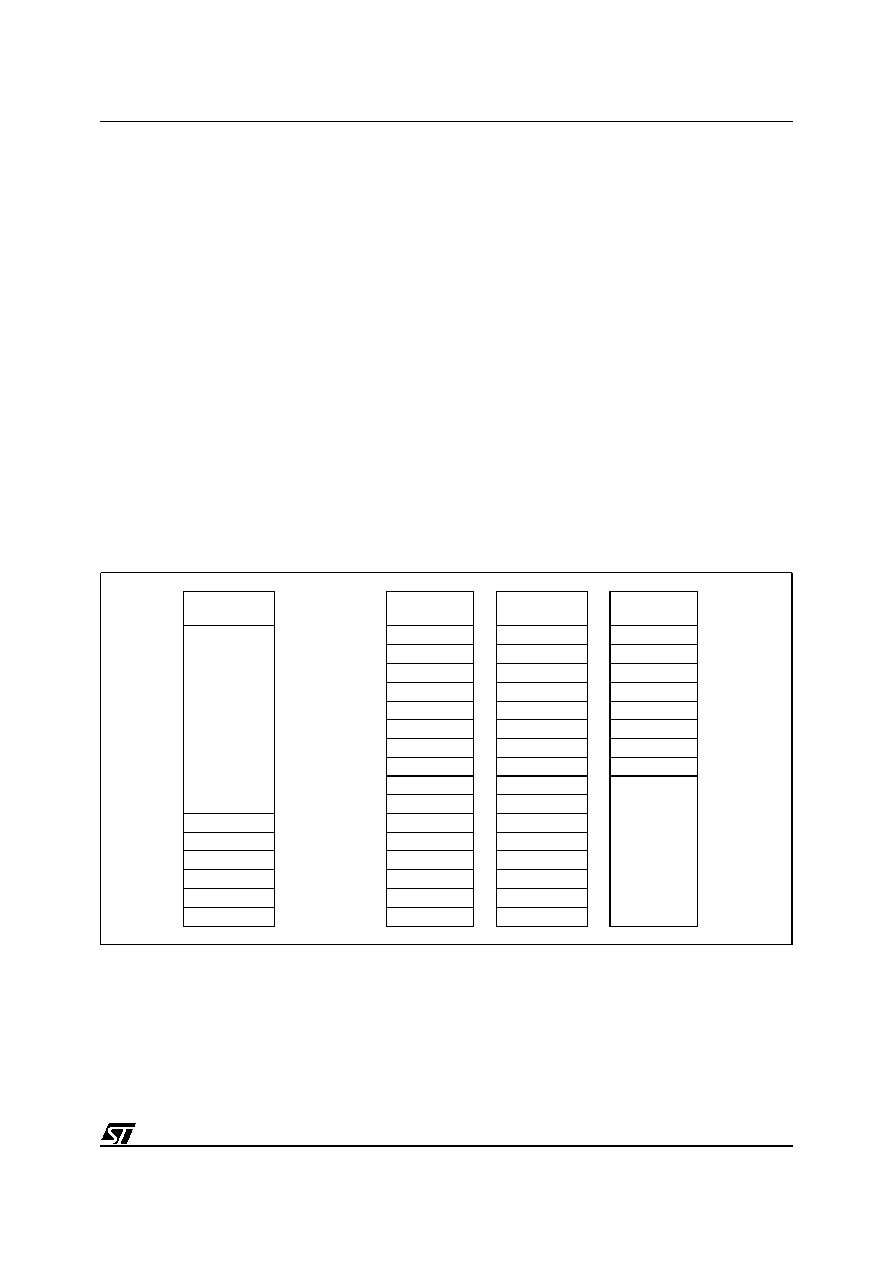
99/230
ST92163 - I/O PORTS
7 I/O PORTS
7.1 INTRODUCTION
ST9 devices feature flexible individually program-
mable multifunctional input/output lines. Refer to
the Pin Description Chapter for specific pin alloca-
tions. These lines, which are logically grouped as
8-bit ports, can be individually programmed to pro-
vide digital input/output and analog input, or to
connect input/output signals to the on-chip periph-
erals as alternate pin functions. All ports can be in-
dividually configured as an input, bi-directional,
output or alternate function. In addition, pull-ups
can be turned off for open-drain operation, and
weak pull-ups can be turned on in their place, to
avoid the need for off-chip resistive pull-ups. Ports
configured as open drain must never have voltage
on the port pin exceeding V
DD
(refer to the Electri-
cal Characteristics section). Depending on the
specific port, input buffers are software selectable
to be TTL or CMOS compatible, however on Sch-
mitt trigger ports, no selection is possible.
7.2 SPECIFIC PORT CONFIGURATIONS
Refer to the Pin Description chapter for a list of the
specific port styles and reset values.
7.3 PORT CONTROL REGISTERS
Each port is associated with a Data register
(PxDR) and three Control registers (PxC0, PxC1,
PxC2). These define the port configuration and al-
low dynamic configuration changes during pro-
gram execution. Port Data and Control registers
are mapped into the Register File as shown in
Fig-
ure 56
. Port Data and Control registers are treated
just like any other general purpose register. There
are no special instructions for port manipulation:
any instruction that can address a register, can ad-
dress the ports. Data can be directly accessed in
the port register, without passing through other
memory or "accumulator" locations.
Figure 56. I/O Register Map
GROUP E
GROUP F
PAGE 2
GROUP F
PAGE 3
GROUP F
PAGE 43
System
Registers
FFh
Reserved
P7DR
P9DR
R255
FEh
P3C2
P7C2
P9C2
R254
FDh
P3C1
P7C1
P9C1
R253
FCh
P3C0
P7C0
P9C0
R252
FBh
Reserved
P6DR
P8DR
R251
FAh
P2C2
P6C2
P8C2
R250
F9h
P2C1
P6C1
P8C1
R249
F8h
P2C0
P6C0
P8C0
R248
F7h
Reserved
Reserved
Reserved
R247
F6h
P1C2
P5C2
R246
E5h
P5DR
R229
F5h
P1C1
P5C1
R245
E4h
P4DR
R228
F4h
P1C0
P5C0
R244
E3h
P3DR
R227
F3h
Reserved
Reserved
R243
E2h
P2DR
R226
F2h
P0C2
P4C2
R242
E1h
P1DR
R225
F1h
P0C1
P4C1
R241
E0h
P0DR
R224
F0h
P0C0
P4C0
R240

100/230
ST92163 - I/O PORTS
PORT CONTROL REGISTERS (Cont'd)
During Reset, ports with weak pull-ups are set in
bidirectional/weak pull-up mode and the output
Data Register is set to FFh. This condition is also
held after Reset, except for Ports 0 and 1 in ROM-
less devices, and can be redefined under software
control.
Bidirectional ports without weak pull-ups are set in
high impedance during reset. To ensure proper
levels during reset, these ports must be externally
connected to either V
DD
or V
SS
through external
pull-up or pull-down resistors.
Other reset conditions may apply in specific ST9
devices.
7.4 INPUT/OUTPUT BIT CONFIGURATION
By programming the control bits PxC0.n and
PxC1.n (see
Figure 57
) it is possible to configure
bit Px.n as Input, Output, Bidirectional or Alternate
Function Output, where X is the number of the I/O
port, and n the bit within the port (n = 0 to 7).
When programmed as input, it is possible to select
the input level as TTL or CMOS compatible by pro-
gramming the relevant PxC2.n control bit.
This option is not available on Schmitt trigger ports.
The output buffer can be programmed as push-
pull or open-drain.
A weak pull-up configuration can be used to avoid
external pull-ups when programmed as bidirec-
tional (except where the weak pull-up option has
been permanently disabled in the pin hardware as-
signment).
Each pin of an I/O port may assume software pro-
grammable Alternate Functions (refer to the de-
vice Pin Description and to Section 7.5). To output
signals from the ST9 peripherals, the port must be
configured as AF OUT. On ST9 devices with A/D
Converter(s), configure the ports used for analog
inputs as AF IN.
The basic structure of the bit Px.n of a general pur-
pose port Px is shown in
Figure 58
.
Independently of the chosen configuration, when
the user addresses the port as the destination reg-
ister of an instruction, the port is written to and the
data is transferred from the internal Data Bus to
the Output Master Latches. When the port is ad-
dressed as the source register of an instruction,
the port is read and the data (stored in the Input
Latch) is transferred to the internal Data Bus.
When Px.n is programmed as an Input:
(See
Figure 59
).
≠ The Output Buffer is forced tristate.
≠ The data present on the I/O pin is sampled into
the Input Latch at the beginning of each instruc-
tion execution.
≠ The data stored in the Output Master Latch is
copied into the Output Slave Latch at the end of
the execution of each instruction. Thus, if bit Px.n
is reconfigured as an Output or Bidirectional, the
data stored in the Output Slave Latch will be re-
flected on the I/O pin.
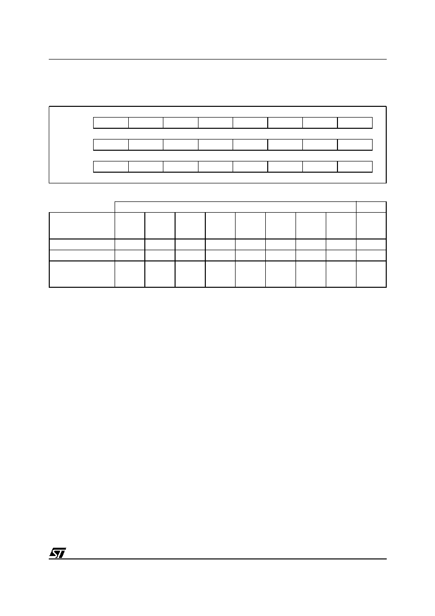
101/230
ST92163 - I/O PORTS
INPUT/OUTPUT BIT CONFIGURATION (Cont'd)
Figure 57. Control Bits
n
Table 18. Port Bit Configuration Table (n = 0, 1... 7; X = port number)
(1)
For A/D Converter inputs.
Legend:
X
= Port
n
= Bit
AF
= Alternate Function
BID
= Bidirectional
CMOS= CMOS Standard Input Levels
HI-Z
= High Impedance
IN
= Input
OD
= Open Drain
OUT = Output
PP
= Push-Pull
TTL
= TTL Standard Input Levels
WP
= Weak Pull-up
Bit 7
Bit n
Bit 0
PxC2
PxC27
PxC2n
PxC20
PxC1
PxC17
PxC1n
PxC10
PxC0
PxC07
PxC0n
PxC00
General Purpose I/O Pins
A/D Pins
PXC2n
PXC1n
PXC0n
0
0
0
1
0
0
0
1
0
1
1
0
0
0
1
1
0
1
0
1
1
1
1
1
1
1
1
PXn Configuration
BID
BID
OUT
OUT
IN
IN
AF OUT
AF OUT
AF IN
PXn Output Type
WP OD
OD
PP
OD
HI-Z
HI-Z
PP
OD
HI-Z
(1)
PXn Input Type
TTL
(or Schmitt
Trigger)
TTL
(or Schmitt
Trigger)
TTL
(or Schmitt
Trigger)
TTL
(or Schmitt
Trigger)
CMOS
(or Schmitt
Trigger)
TTL
(or Schmitt
Trigger)
TTL
(or Schmitt
Trigger)
TTL
(or Schmitt
Trigger)
Analog
Input
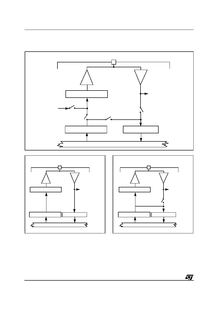
102/230
ST92163 - I/O PORTS
INPUT/OUTPUT BIT CONFIGURATION (Cont'd)
Figure 58. Basic Structure of an I/O Port Pin
Figure 59. Input Configuration
n
n
Figure 60. Output Configuration
n
OUTPUT SLAVE LATCH
OUTPUT MASTER LATCH
INPUT LATCH
INTERNAL DATA BUS
I/O PIN
PUSH-PULL
TRISTATE
OPEN DRAIN
WEAK PULL-UP
FROM
PERIPHERAL
OUTPUT
OUTPUT
INPUT
BIDIRECTIONAL
ALTERNATE
FUNCTION
TO PERIPHERAL
INPUTS AND
TTL / CMOS
(or Schmitt Trigger)
INTERRUPTS
ALTERNATE
FUNCTION
INPUT
OUTPUT
BIDIRECTIONAL
OUTPUT MASTER LATCH
INPUT LATCH
OUTPUT SLAVE LATCH
INTERNAL DATA BUS
I/O PIN
TRISTATE
TO PERIPHERAL
INPUTS AND
TTL / CMOS
(or Schmitt Trigger)
INTERRUPTS
OUTPUT MASTER LATCH
INPUT LATCH
OUTPUT SLAVE LATCH
INTERNAL DATA BUS
I/O PIN
OPEN DRAIN
TTL
(or Schmitt Trigger)
PUSH-PULL
TO PERIPHERAL
INPUTS AND
INTERRUPTS
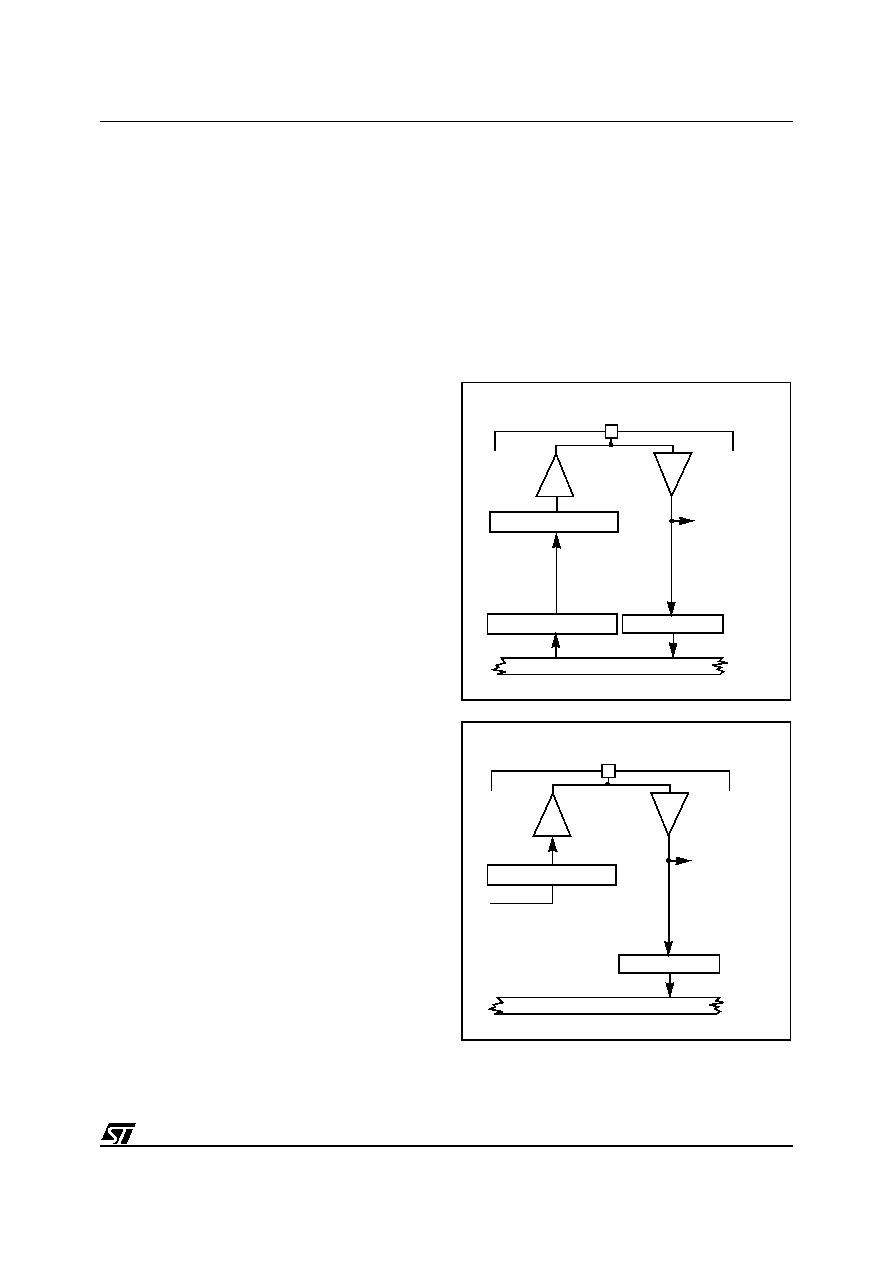
103/230
ST92163 - I/O PORTS
INPUT/OUTPUT BIT CONFIGURATION (Cont'd)
When Px.n is programmed as an Output:
(
Figure 60
)
≠ The Output Buffer is turned on in an Open-drain
or Push-pull configuration.
≠ The data stored in the Output Master Latch is
copied both into the Input Latch and into the Out-
put Slave Latch, driving the I/O pin, at the end of
the execution of the instruction.
When Px.n is programmed as Bidirectional:
(
Figure 61
)
≠ The Output Buffer is turned on in an Open-Drain
or Weak Pull-up configuration (except when dis-
abled in hardware).
≠ The data present on the I/O pin is sampled into
the Input Latch at the beginning of the execution
of the instruction.
≠ The data stored in the Output Master Latch is
copied into the Output Slave Latch, driving the I/
O pin, at the end of the execution of the instruc-
tion.
WARNING: Due to the fact that in bidirectional
mode the external pin is read instead of the output
latch, particular care must be taken with arithme-
tic/logic and Boolean instructions performed on a
bidirectional port pin.
These instructions use a read-modify-write se-
quence, and the result written in the port register
depends on the logical level present on the exter-
nal pin.
This may bring unwanted modifications to the port
output register content.
For example:
Port register content, 0Fh
external port value, 03h
(Bits 3 and 2 are externally forced to 0)
A
bset
instruction on bit 7 will return:
Port register content, 83h
external port value, 83h
(Bits 3 and 2 have been cleared).
To avoid this situation, it is suggested that all oper-
ations on a port, using at least one bit in bidirec-
tional mode, are performed on a copy of the port
register, then transferring the result with a load in-
struction to the I/O port.
When Px.n is programmed as a digital Alter-
nate Function Output:
(
Figure 62
)
≠ The Output Buffer is turned on in an Open-Drain
or Push-Pull configuration.
≠ The data present on the I/O pin is sampled into
the Input Latch at the beginning of the execution
of the instruction.
≠ The signal from an on-chip function is allowed to
load the Output Slave Latch driving the I/O pin.
Signal timing is under control of the alternate
function. If no alternate function is connected to
Px.n, the I/O pin is driven to a high level when in
Push-Pull configuration, and to a high imped-
ance state when in open drain configuration.
Figure 61. Bidirectional Configuration
n
n
Figure 62. Alternate Function Configuration
n
n
n
n
n
n
OUTPUT MASTER LATCH
INPUT LATCH
OUTPUT SLAVE LATCH
INTERNAL DATA BUS
I/O PIN
WEAK PULL-UP
TTL
(or Schmitt Trigger)
OPEN DRAIN
TO PERIPHERAL
INPUTS AND
INTERRUPTS
INPUT LATCH
FROM
INTERNAL DATA BUS
I/O PIN
OPEN DRAIN
TTL
(or Schmitt Trigger)
PUSH-PULL
PERIPHERAL
OUTPUT
TO PERIPHERAL
INPUTS AND
INTERRUPTS
OUTPUT SLAVE LATCH
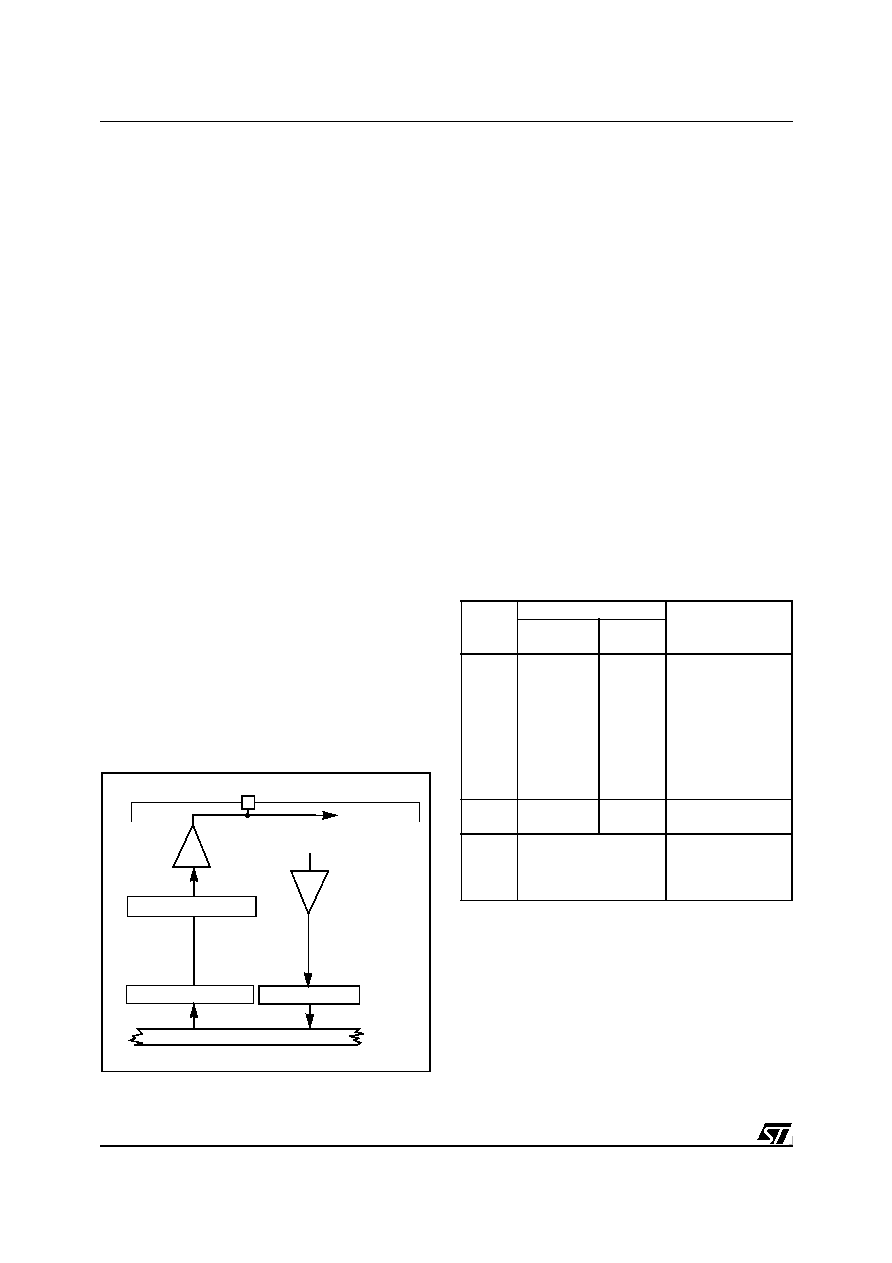
104/230
ST92163 - ALTERNATE FUNCTION ARCHITECTURE
7.5 ALTERNATE FUNCTION ARCHITECTURE
Each I/O pin may be connected to three different
types of internal signal:
≠ Data bus Input/Output
≠ Alternate Function Input
≠ Alternate Function Output
7.5.1 Pin Declared as I/O
A pin declared as I/O, is connected to the I/O buff-
er. This pin may be an Input, an Output, or a bidi-
rectional I/O, depending on the value stored in
(PxC2, PxC1 and PxC0).
7.5.2 Pin Declared as an Alternate Function
Input
A single pin may be directly connected to several
Alternate Function inputs. In this case, the user
must select the required input mode (with the
PxC2, PxC1, PxC0 bits) and enable the selected
Alternate Function in the Control Register of the
peripheral. No specific port configuration is re-
quired to enable an Alternate Function input, since
the input buffer is directly connected to each alter-
nate function module on the shared pin. As more
than one module can use the same input, it is up to
the user software to enable the required module
as necessary. Parallel I/Os remain operational
even when using an Alternate Function input. The
exception to this is when an I/O port bit is perma-
nently assigned by hardware as an A/D bit. In this
case , after software programming of the bit in AF-
OD-TTL, the Alternate function output is forced to
logic level 1. The analog voltage level on the cor-
responding pin is directly input to the A/D (See
Fig-
ure 63
).
Figure 63. A/D Input Configuration
7.5.3 Pin Declared as an Alternate Function
Output
The user must select the AF OUT configuration
using the PxC2, PxC1, PxC0 bits. Several Alter-
nate Function outputs may drive a common pin. In
such case, the Alternate Function output signals
are logically ANDed before driving the common
pin. The user must therefore enable the required
Alternate Function Output by software.
WARNING: When a pin is connected both to an al-
ternate function output and to an alternate function
input, it should be noted that the output signal will
always be present on the alternate function input.
7.6 I/O STATUS AFTER WFI, HALT AND RESET
The status of the I/O ports during the Wait For In-
terrupt, Halt and Reset operational modes is
shown in the following table. The External Memory
Interface ports are shown separately. If only the in-
ternal memory is being used and the ports are act-
ing as I/O, the status is the same as shown for the
other I/O ports.
INPUT LATCH
INTERNAL DATA BUS
I/O PIN
TRISTATE
INPUT
BUFFER
OUTPUT SLAVE LATCH
OUTPUT MASTER LATCH
TOWARDS
A/D CONVERTER
GND
Mode
Ext. Mem - I/O Ports
I/O Ports
P0
P1, P2,
P6, P9
WFI
High Imped-
ance or next
address (de-
pending on
the last
memory op-
eration per-
formed on
Port)
Next
Address
Not Affected (clock
outputs running)
HALT
High Imped-
ance
Next
Address
Not Affected (clock
outputs stopped)
RESET
Alternate function push-
pull (ROMless device)
Bidirectional Weak
Pull-up (High im-
pedance when disa-
bled in hardware).
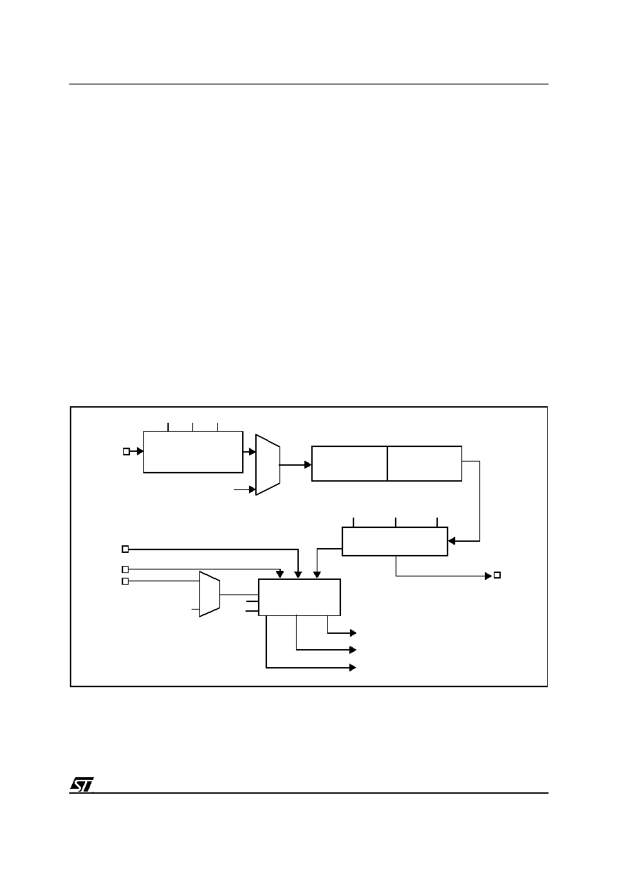
105/230
ST92163 - TIMER/WATCHDOG (WDT)
8 ON-CHIP PERIPHERALS
8.1 TIMER/WATCHDOG (WDT)
Important Note: This chapter is a generic descrip-
tion of the WDT peripheral. However depending
on the ST9 device, some or all of WDT interface
signals described may not be connected to exter-
nal pins. For the list of WDT pins present on the
ST9 device, refer to the device pinout description
in the first section of the data sheet.
8.1.1 Introduction
The Timer/Watchdog (WDT) peripheral consists of
a programmable 16-bit timer and an 8-bit prescal-
er. It can be used, for example, to:
≠ Generate periodic interrupts
≠ Measure input signal pulse widths
≠ Request an interrupt after a set number of events
≠ Generate an output signal waveform
≠ Act as a Watchdog timer to monitor system in-
tegrity
The main WDT registers are:
≠ Control register for the input, output and interrupt
logic blocks (WDTCR)
≠ 16-bit counter register pair (WDTHR, WDTLR)
≠ Prescaler register (WDTPR)
The hardware interface consists of up to five sig-
nals:
≠ WDIN External clock input
≠ WDOUT Square wave or PWM signal output
≠ INT0 External interrupt input
≠ NMI Non-Maskable Interrupt input
≠ HW0SW1 Hardware/Software Watchdog ena-
ble.
Figure 64. Timer/Watchdog Block Diagram
INT0
1
INPUT
&
CLOCK CONTROL LOGIC
INEN INMD1 INMD2
WDTPR
8-BIT PRESCALER
WDTRH, WDTRL
16-BIT
INTCLK/4
WDT
OUTMD
WROUT
OUTPUT CONTROL LOGIC
INTERRUPT
CONTROL LOGIC
END OF
COUNT
RESET
TOP LEVEL INTERRUPT REQUEST
OUTEN
MUX
WDOUT
1
IAOS
TLIS
INTA0 REQUEST
NMI
1
WDGEN
HW0SW1
1
WDIN
1
MUX
DOWNCOUNTER
CLOCK
1
Pin not present on some ST9 devices
.

106/230
ST92163 - TIMER/WATCHDOG (WDT)
TIMER/WATCHDOG (Cont'd)
8.1.2 Functional Description
8.1.2.1 External Signals
The HW0SW1 pin can be used to permanently en-
able Watchdog mode. Refer to section 8.1.3.1 on
page 107.
The WDIN Input pin can be used in one of four
modes:
≠ Event Counter Mode
≠ Gated External Input Mode
≠ Triggerable Input Mode
≠ Retriggerable Input Mode
The WDOUT output pin can be used to generate a
square wave or a Pulse Width Modulated signal.
An interrupt, generated when the WDT is running
as the 16-bit Timer/Counter, can be used as a Top
Level Interrupt or as an interrupt source connected
to channel A0 of the external interrupt structure
(replacing the INT0 interrupt input).
The counter can be driven either by an external
clock, or internally by INTCLK divided by 4.
8.1.2.2 Initialisation
The prescaler (WDTPR) and counter (WDTRL,
WDTRH) registers must be loaded with initial val-
ues before starting the Timer/Counter. If this is not
done, counting will start with reset values.
8.1.2.3 Start/Stop
The ST_SP bit enables downcounting. When this
bit is set, the Timer will start at the beginning of the
following instruction. Resetting this bit stops the
counter.
If the counter is stopped and restarted, counting
will resume from the last value unless a new con-
stant has been entered in the Timer registers
(WDTRL, WDTRH).
A new constant can be written in the WDTRH,
WDTRL, WDTPR registers while the counter is
running. The new value of the WDTRH, WDTRL
registers will be loaded at the next End of Count
(EOC) condition while the new value of the
WDTPR register will be effective immediately.
End of Count is when the counter is 0.
When Watchdog mode is enabled the state of the
ST_SP bit is irrelevant.
8.1.2.4 Single/Continuous Mode
The S_C bit allows selection of single or continu-
ous mode.This Mode bit can be written with the
Timer stopped or running. It is possible to toggle
the S_C bit and start the counter with the same in-
struction.
Single Mode
On reaching the End Of Count condition, the Timer
stops, reloads the constant, and resets the Start/
Stop bit. Software can check the current status by
reading this bit. To restart the Timer, set the Start/
Stop bit.
Note: If the Timer constant has been modified dur-
ing the stop period, it is reloaded at start time.
Continuous Mode
On reaching the End Of Count condition, the coun-
ter automatically reloads the constant and restarts.
It is stopped only if the Start/Stop bit is reset.
8.1.2.5 Input Section
If the Timer/Counter input is enabled (INEN bit) it
can count pulses input on the WDIN pin. Other-
wise it counts the internal clock/4.
For instance, when INTCLK = 24MHz, the End Of
Count rate is:
2.79 seconds for Maximum Count
(Timer Const. = FFFFh, Prescaler Const. = FFh)
166 ns for Minimum Count
(Timer Const. = 0000h, Prescaler Const. = 00h)
The Input pin can be used in one of four modes:
≠ Event Counter Mode
≠ Gated External Input Mode
≠ Triggerable Input Mode
≠ Retriggerable Input Mode
The mode is configurable in the WDTCR.
8.1.2.6 Event Counter Mode
In this mode the Timer is driven by the external
clock applied to the input pin, thus operating as an
event counter. The event is defined as a high to
low transition of the input signal. Spacing between
trailing edges should be at least 8 INTCLK periods
(or 333ns with INTCLK = 24MHz).
Counting starts at the next input event after the
ST_SP bit is set and stops when the ST_SP bit is
reset.

107/230
ST92163 - TIMER/WATCHDOG (WDT)
TIMER/WATCHDOG (Cont'd)
8.1.2.7 Gated Input Mode
This mode can be used for pulse width measure-
ment. The Timer is clocked by INTCLK/4, and is
started and stopped by means of the input pin and
the ST_SP bit. When the input pin is high, the Tim-
er counts. When it is low, counting stops. The
maximum input pin frequency is equivalent to
INTCLK/8.
8.1.2.8 Triggerable Input Mode
The Timer (clocked internally by INTCLK/4) is
started by the following sequence:
≠ setting the Start-Stop bit, followed by
≠ a High to Low transition on the input pin.
To stop the Timer, reset the ST_SP bit.
8.1.2.9 Retriggerable Input Mode
In this mode, the Timer (clocked internally by
INTCLK/4) is started by setting the ST_SP bit. A
High to Low transition on the input pin causes
counting to restart from the initial value. When the
Timer is stopped (ST_SP bit reset), a High to Low
transition of the input pin has no effect.
8.1.2.10 Timer/Counter Output Modes
Output modes are selected by means of the OUT-
EN (Output Enable) and OUTMD (Output Mode)
bits of the WDTCR register.
No Output Mode
(OUTEN = "0")
The output is disabled and the corresponding pin
is set high, in order to allow other alternate func-
tions to use the I/O pin.
Square Wave Output Mode
(OUTEN = "1", OUTMD = "0")
The Timer outputs a signal with a frequency equal
to half the End of Count repetition rate on the WD-
OUT pin. With an INTCLK frequency of 20MHz,
this allows a square wave signal to be generated
whose period can range from 400ns to 6.7 sec-
onds.
Pulse Width Modulated Output Mode
(OUTEN = "1", OUTMD = "1")
The state of the WROUT bit is transferred to the
output pin (WDOUT) at the End of Count, and is
held until the next End of Count condition. The
user can thus generate PWM signals by modifying
the status of the WROUT pin between End of
Count events, based on software counters decre-
mented by the Timer Watchdog interrupt.
8.1.3 Watchdog Timer Operation
This mode is used to detect the occurrence of a
software fault, usually generated by external inter-
ference or by unforeseen logical conditions, which
causes the application program to abandon its
normal sequence of operation. The Watchdog,
when enabled, resets the MCU, unless the pro-
gram executes the correct write sequence before
expiry of the programmed time period. The appli-
cation program must be designed so as to correct-
ly write to the WDTLR Watchdog register at regu-
lar intervals during all phases of normal operation.
8.1.3.1 Hardware Watchdog/Software
Watchdog
The HW0SW1 pin (when available) selects Hard-
ware Watchdog or Software Watchdog.
If HW0SW1 is held low:
≠ The Watchdog is enabled by hardware immedi-
ately after an external reset. (Note: Software re-
set or Watchdog reset have no effect on the
Watchdog enable status).
≠ The initial counter value (FFFFh) cannot be mod-
ified, however software can change the prescaler
value on the fly.
≠ The WDGEN bit has no effect. (Note: it is not
forced low).
If HW0SW1 is held high, or is not present:
≠ The Watchdog can be enabled by resetting the
WDGEN bit.
8.1.3.2 Starting the Watchdog
In Watchdog mode the Timer is clocked by
INTCLK/4.
If the Watchdog is software enabled, the time base
must be written in the timer registers before enter-
ing Watchdog mode by resetting the WDGEN bit.
Once reset, this bit cannot be changed by soft-
ware.
If the Watchdog is hardware enabled, the time
base is fixed by the reset value of the registers.
Resetting WDGEN causes the counter to start, re-
gardless of the value of the Start-Stop bit.
In Watchdog mode, only the Prescaler Constant
may be modified.
If the End of Count condition is reached a System
Reset is generated.
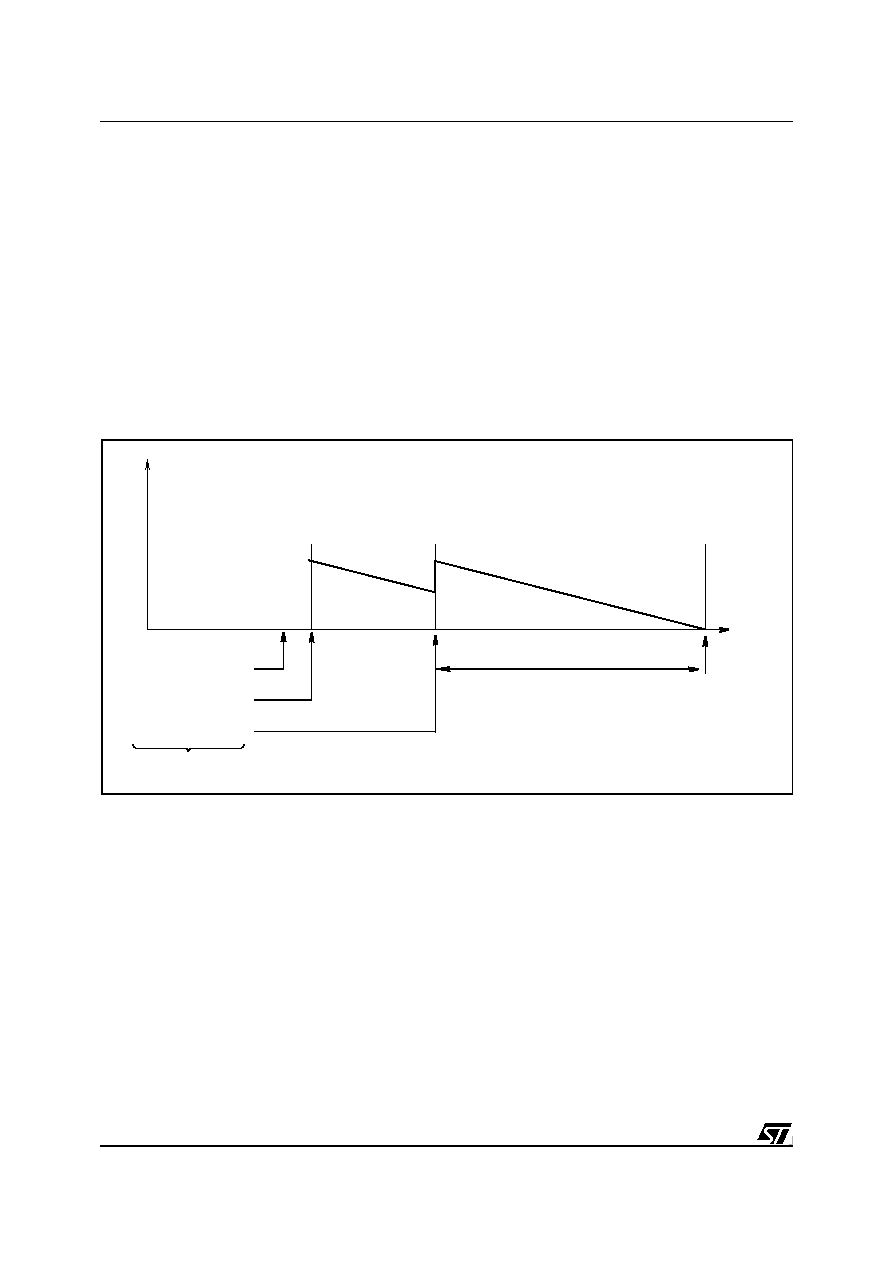
108/230
ST92163 - TIMER/WATCHDOG (WDT)
TIMER/WATCHDOG (Cont'd)
8.1.3.3 Preventing Watchdog System Reset
In order to prevent a system reset, the sequence
AAh, 55h must be written to WDTLR (Watchdog
Timer Low Register). Once 55h has been written,
the Timer reloads the constant and counting re-
starts from the preset value.
To reload the counter, the two writing operations
must be performed sequentially without inserting
other instructions that modify the value of the
WDTLR register between the writing operations.
The maximum allowed time between two reloads
of the counter depends on the Watchdog timeout
period.
8.1.3.4 Non-Stop Operation
In Watchdog Mode, a
Halt
instruction is regarded
as illegal. Execution of the
Halt
instruction stops
further execution by the CPU and interrupt ac-
knowledgment, but does not stop INTCLK, CPU-
CLK or the Watchdog Timer, which will cause a
System Reset when the End of Count condition is
reached. Furthermore, ST_SP, S_C and the Input
Mode selection bits are ignored. Hence, regard-
less of their status, the counter always runs in
Continuous Mode, driven by the internal clock.
The Output mode should not be enabled, since in
this context it is meaningless.
Figure 65. Watchdog Timer Mode
TIMER START COUNTING
WRITE WDTRH,WDTRL
WD EN=0
WRITE AAh,55h
INTO WDTRL
RESET
SOFTWARE FAIL
(E.G. INFINITE LOOP)
OR PERIPHERAL FAIL
VA00220
PRODUCE
COUNT RELOAD
VALUE
COUNT
G
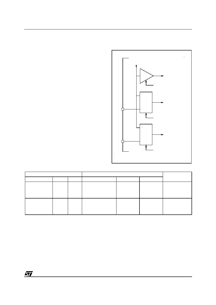
109/230
ST92163 - TIMER/WATCHDOG (WDT)
TIMER/WATCHDOG (Cont'd)
8.1.4 WDT Interrupts
The Timer/Watchdog issues an interrupt request
at every End of Count, when this feature is ena-
bled.
A pair of control bits, IA0S (EIVR.1, Interrupt A0 se-
lection bit) and TLIS (EIVR.2, Top Level Input Se-
lection bit) allow the selection of 2 interrupt sources
(Timer/Watchdog End of Count, or External Pin)
handled in two different ways, as a Top Level Non
Maskable Interrupt (Software Reset), or as a
source for channel A0 of the external interrupt logic.
A block diagram of the interrupt logic is given in
Figure 66
.
Note: Software traps can be generated by setting
the appropriate interrupt pending bit.
Table 19
below, shows all the possible configura-
tions of interrupt/reset sources which relate to the
Timer/Watchdog.
A reset caused by the watchdog will set bit 6,
WDGRES of R242 - Page 55 (Clock Flag Regis-
ter). See
section CLOCK CONTROL REGIS-
TERS
.
Figure 66. Interrupt Sources
Table 19. Interrupt Configuration
Legend:
WDG = Watchdog function
SW TRAP = Software Trap
Note: If IA0S and TLIS = 0 (enabling the Watchdog EOC as interrupt source for both Top Level and INTA0
interrupts), only the INTA0 interrupt is taken into account.
TIMER WATCHDOG
RESET
WDGEN (WCR.6)
INTA0 REQUEST
IA0S (EIVR.1)
MUX
0
1
INT0
MUX
0
1
TOP LEVEL
INTERRUPT REQUEST
VA00293
TLIS (EIVR.2)
NMI
Control Bits
Enabled Sources
Operating Mode
WDGEN
IA0S
TLIS
Reset
INTA0
Top Level
0
0
0
0
0
0
1
1
0
1
0
1
WDG/Ext Reset
WDG/Ext Reset
WDG/Ext Reset
WDG/Ext Reset
SW TRAP
SW TRAP
Ext Pin
Ext Pin
SW TRAP
Ext Pin
SW TRAP
Ext Pin
Watchdog
Watchdog
Watchdog
Watchdog
1
1
1
1
0
0
1
1
0
1
0
1
Ext Reset
Ext Reset
Ext Reset
Ext Reset
Timer
Timer
Ext Pin
Ext Pin
Timer
Ext Pin
Timer
Ext Pin
Timer
Timer
Timer
Timer
110/230
ST92163 - TIMER/WATCHDOG (WDT)
TIMER/WATCHDOG (Cont'd)
8.1.5 Register Description
The Timer/Watchdog is associated with 4 registers
mapped into Group F, Page 0 of the Register File.
WDTHR: Timer/Watchdog High Register
WDTLR: Timer/Watchdog Low Register
WDTPR: Timer/Watchdog Prescaler Register
WDTCR: Timer/Watchdog Control Register
Three additional control bits are mapped in the fol-
lowing registers on Page 0:
Watchdog Mode Enable, (WCR.6)
Top Level Interrupt Selection, (EIVR.2)
Interrupt A0 Channel Selection, (EIVR.1)
Note: The registers containing these bits also con-
tain other functions. Only the bits relevant to the
operation of the Timer/Watchdog are shown here.
Counter Register
This 16-bit register (WDTLR, WDTHR) is used to
load the 16-bit counter value. The registers can be
read or written "on the fly".
TIMER/WATCHDOG HIGH REGISTER (WDTHR)
R248 - Read/Write
Register Page: 0
Reset value: 1111 1111 (FFh)
Bits
7:0 = R[15:8]
Counter Most Significant Bits
.
TIMER/WATCHDOG LOW REGISTER (WDTLR)
R249 - Read/Write
Register Page: 0
Reset value: 1111 1111b (FFh)
Bits
7:0 = R[7:0]
Counter Least Significant Bits.
TIMER/WATCHDOG PRESCALER REGISTER
(WDTPR)
R250 - Read/Write
Register Page: 0
Reset value: 1111 1111 (FFh)
Bits 7:0 = PR[7:0]
Prescaler value.
A programmable value from 1 (00h) to 256 (FFh).
Warning
:
In order to prevent incorrect operation of
the Timer/Watchdog, the prescaler (WDTPR) and
counter (WDTRL, WDTRH) registers must be ini-
tialised before starting the Timer/Watchdog. If this
is not done, counting will start with the reset (un-in-
itialised) values.
WATCHDOG TIMER CONTROL REGISTER
(WDTCR)
R251- Read/Write
Register Page: 0
Reset value: 0001 0010 (12h)
Bit
7 = ST_SP:
Start/Stop Bit
.
This bit is set and cleared by software.
0: Stop counting
1: Start counting (see Warning above)
Bit 6 = S_C:
Single/Continuous
.
This bit is set and cleared by software.
0: Continuous Mode
1: Single Mode
Bits 5:4 = INMD[1:2]:
Input mode selection bits
.
These bits select the input mode:
7
0
R15
R14
R13
R12
R11
R10
R9
R8
7
0
R7
R6
R5
R4
R3
R2
R1
R0
7
0
PR7
PR6
PR5
PR4
PR3
PR2
PR1
PR0
7
0
ST_SP
S_C
INMD1
INMD2
INEN
OUTMD
WROUT
OUTEN
INMD1
INMD2
INPUT MODE
0
0
Event Counter
0
1
Gated Input (Reset value)
1
0
Triggerable Input
1
1
Retriggerable Input

111/230
ST92163 - TIMER/WATCHDOG (WDT)
TIMER/WATCHDOG (Cont'd)
Bit 3 = INEN:
Input Enable
.
This bit is set and cleared by software.
0: Disable input section
1: Enable input section
Bit 2 = OUTMD:
Output Mode.
This bit is set and cleared by software.
0: The output is toggled at every End of Count
1: The value of the WROUT bit is transferred to the
output pin on every End Of Count if OUTEN=1.
Bit 1 = WROUT:
Write Out
.
The status of this bit is transferred to the Output
pin when OUTMD is set; it is user definable to al-
low PWM output (on Reset WROUT is set).
Bit 0 = OUTEN:
Output Enable bit
.
This bit is set and cleared by software.
0: Disable output
1: Enable output
WAIT CONTROL REGISTER (WCR)
R252 - Read/Write
Register Page: 0
Reset value: 0111 1111 (7Fh)
Bit 6 = WDGEN:
Watchdog Enable
(active low).
Resetting this bit via software enters the Watch-
dog mode. Once reset, it cannot be set anymore
by the user program. At System Reset, the Watch-
dog mode is disabled.
Note: This bit is ignored if the Hardware Watchdog
option is enabled by pin HW0SW1 (if available).
EXTERNAL INTERRUPT VECTOR REGISTER
(EIVR)
R246 - Read/Write
Register Page: 0
Reset value: xxxx 0110 (x6h)
Bit 2 = TLIS:
Top Level Input Selection
.
This bit is set and cleared by software.
0: Watchdog End of Count is TL interrupt source
1: NMI is TL interrupt source
Bit 1 = IA0S:
Interrupt Channel A0 Selection.
This bit is set and cleared by software.
0: Watchdog End of Count is INTA0 source
1: External Interrupt pin is INTA0 source
Warning
:
To avoid spurious interrupt requests,
the IA0S bit should be accessed only when the in-
terrupt logic is disabled (i.e. after the DI instruc-
tion). It is also necessary to clear any possible in-
terrupt pending requests on channel A0 before en-
abling this interrupt channel. A delay instruction
(e.g. a NOP instruction) must be inserted between
the reset of the interrupt pending bit and the IA0S
write instruction.
Other bits are described in the Interrupt section.
7
0
x
WDGEN
x
x
x
x
x
x
7
0
x
x
x
x
x
TLIS
IA0S
x
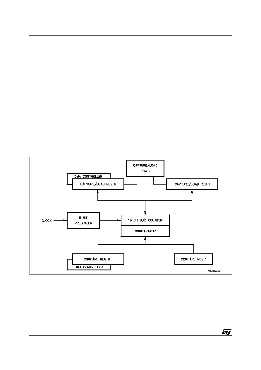
112/230
ST92163 - MULTIFUNCTION TIMER (MFT)
8.2 MULTIFUNCTION TIMER (MFT)
8.2.1 Introduction
The Multifunction Timer (MFT) peripheral offers
powerful timing capabilities and features 12 oper-
ating modes, including automatic PWM generation
and frequency measurement.
The MFT comprises a 16-bit Up/Down counter
driven by an 8-bit programmable prescaler. The in-
put clock may be INTCLK/3 or an external source.
The timer features two 16-bit Comparison Regis-
ters, and two 16-bit Capture/Load/Reload Regis-
ters. Two input pins and two alternate function out-
put pins are available.
Several functional configurations are possible, for
instance:
≠ 2 input captures on separate external lines, and
2 independent output compare functions with the
counter in free-running mode, or 1 output com-
pare at a fixed repetition rate.
≠ 1 input capture, 1 counter reload and 2 inde-
pendent output compares.
≠ 2 alternate autoreloads and 2 independent out-
put compares.
≠ 2 alternate captures on the same external line
and 2 independent output compares at a fixed
repetition rate.
When two MFTs are present in an ST9 device, a
combined operating mode is available.
An internal On-Chip Event signal can be used on
some devices to control other on-chip peripherals.
The two external inputs may be individually pro-
grammed to detect any of the following:
≠ rising edges
≠ falling edges
≠ both rising and falling edges
Figure 67. MFT Simplified Block Diagram
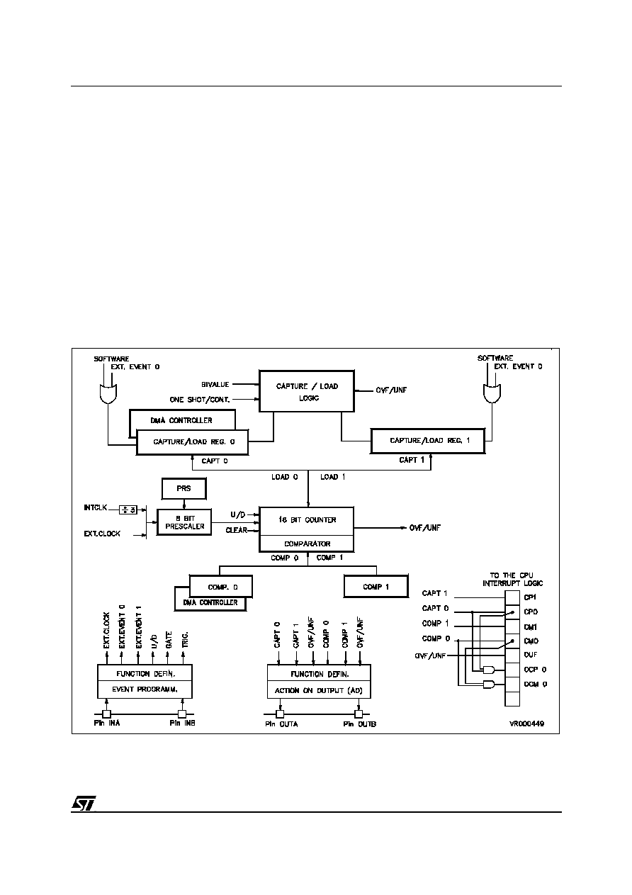
113/230
ST92163 - MULTIFUNCTION TIMER (MFT)
MULTIFUNCTION TIMER (Cont'd)
The configuration of each input is programmed in
the Input Control Register.
Each of the two output pins can be driven from any
of three possible sources:
≠ Compare Register 0 logic
≠ Compare Register 1 logic
≠ Overflow/Underflow logic
Each of these three sources can cause one of the
following four actions, independently, on each of
the two outputs:
≠ Nop, Set, Reset, Toggle
In addition, an additional On-Chip Event signal can
be generated by two of the three sources men-
tioned above, i.e. Over/Underflow event and Com-
pare 0 event. This signal can be used internally to
synchronise another on-chip peripheral. Five
maskable interrupt sources referring to an End Of
Count condition, 2 input captures and 2 output
compares, can generate 3 different interrupt re-
quests (with hardware fixed priority), pointing to 3
interrupt routine vectors.
Two independent DMA channels are available for
rapid data transfer operations. Each DMA request
(associated with a capture on the REG0R register,
or with a compare on the CMP0R register) has pri-
ority over an interrupt request generated by the
same source.
A SWAP mode is also available to allow high
speed continuous transfers (see Interrupt and
DMA chapter).
Figure 68. Detailed Block Diagram

114/230
ST92163 - MULTIFUNCTION TIMER (MFT)
MULTIFUNCTION TIMER (Cont'd)
8.2.2 Functional Description
The MFT operating modes are selected by pro-
gramming the Timer Control Register (TCR) and
the Timer Mode Register (TMR).
8.2.2.1 Trigger Events
A trigger event may be generated by software (by
setting either the CP0 or the CP1 bits in the
T_FLAGR register) or by an external source which
may be programmed to respond to the rising edge,
the falling edge or both by programming bits A0-
A1 and B0-B1 in the T_ICR register. This trigger
event can be used to perform a capture or a load,
depending on the Timer mode (configured using
the bits in
Table 4
).
An event on the TxINA input or setting the CP0 bit
triggers a capture to, or a load from the REG0R
register (except in Bicapture mode, see
Section
0.1.2.11
).
An event on the TxINB input or setting the CP1 bit
triggers a capture to, or a load from the REG1R
register.
In addition, in the special case of "Load from
REG0R and monitor on REG1R", it is possible to
use the TxINB input as a trigger for REG0R."
8.2.2.2 One Shot Mode
When the counter generates an overflow (in up-
count mode), or an underflow (in down-count
mode), that is to say when an End Of Count condi-
tion is reached, the counter stops and no counter
reload occurs. The counter may only be restarted
by an external trigger on TxINA or B or a by soft-
ware trigger on CP0 only. One Shot Mode is en-
tered by setting the CO bit in TMR.
8.2.2.3 Continuous Mode
Whenever the counter reaches an End Of Count
condition, the counting sequence is automatically
restarted and the counter is reloaded from REG0R
(or from REG1R, when selected in Biload Mode).
Continuous Mode is entered by resetting the C0 bit
in TMR.
8.2.2.4 Triggered And Retriggered Modes
A triggered event may be generated by software
(by setting either the CP0 or the CP1 bit in the
T_FLAGR register), or by an external source
which may be programmed to respond to the rising
edge, the falling edge or both, by programming
bits A0-A1 and B0-B1 in T_ICR.
In One Shot and Triggered Mode, every trigger
event arriving before an End Of Count, is masked.
In One Shot and Retriggered Mode, every trigger
received while the counter is running, automatical-
ly reloads the counter from REG0R. Triggered/Re-
triggered Mode is set by the REN bit in TMR.
The TxINA input refers to REG0R and the TxINB
input refers to REG1R.
WARNING. If the Triggered Mode is selected
when the counter is in Continuous Mode, every
trigger is disabled, it is not therefore possible to
synchronise the counting cycle by hardware or
software.
8.2.2.5 Gated Mode
In this mode, counting takes place only when the
external gate input is at a logic low level. The se-
lection of TxINA or TxINB as the gate input is
made by programming the IN0-IN3 bits in T_ICR.
8.2.2.6 Capture Mode
The REG0R and REG1R registers may be inde-
pendently set in Capture Mode by setting RM0 or
RM1 in TMR, so that a capture of the current count
value can be performed either on REG0R or on
REG1R, initiated by software (by setting CP0 or
CP1 in the T_FLAGR register) or by an event on
the external input pins.
WARNING. Care should be taken when two soft-
ware captures are to be performed on the same
register. In this case, at least one instruction must
be present between the first CP0/CP1 bit set and
the subsequent CP0/CP1 bit reset instructions.
8.2.2.7 Up/Down Mode
The counter can count up or down depending on
the state of the UDC bit (Up/Down Count) in TCR,
or on the configuration of the external input pins,
which have priority over UDC (see Input pin as-
signment in T_ICR). The UDCS bit returns the
counter up/down current status (see also the Up/
Down Autodiscrimination mode in the Input Pin
Assignment Section).

115/230
ST92163 - MULTIFUNCTION TIMER (MFT)
MULTIFUNCTION TIMER (Cont'd)
8.2.2.8 Free Running Mode
The timer counts continuously (in Up or Down
mode) and the counter value simply overflows or
underflows through FFFFh or zero; there is no End
Of Count condition as such, and no reloading
takes place. This mode is automatically selected
either in Bi-capture mode or by setting register
REG0R for a Capture function (Continuous mode
must also be set). In Autoclear mode, free running
operation can be selected, with the possibility of
choosing a maximum count value less than 2
16
before overflow or underflow (see Autoclear
mode).
8.2.2.9 Monitor Mode
When the RM1 bit in TMR is reset, and the timer is
not in Bi-value mode, REG1R acts as a monitor,
duplicating the current up or down counter con-
tents, thus allowing the counter to be read "on the
fly".
8.2.2.10 Autoclear Mode
A clear command forces the counter either to
0000h or to FFFFh, depending on whether up-
counting or downcounting is selected. The counter
reset may be obtained either directly, through the
CCL bit in TCR, or by entering the Autoclear
Mode, through the CCP0 and CCMP0 bits in TCR.
Every capture performed on REG0R (if CCP0 is
set), or every successful compare performed by
CMP0R (if CCMP0 is set), clears the counter and
reloads the prescaler.
The Clear On Capture mode allows direct meas-
urement of delta time between successive cap-
tures on REG0R, while the Clear On Compare
mode allows free running with the possibility of
choosing a maximum count value before overflow
or underflow which is less than 2
16
(see Free Run-
ning Mode).
8.2.2.11 Bi-value Mode
Depending on the value of the RM0 bit in TMR, the
Bi-load Mode (RM0 reset) or the Bi-capture Mode
(RM0 set) can be selected as illustrated in
Figure 1
below:
Table 20. Bi-value Modes
A) Biload Mode
The Bi-load Mode is entered by selecting the Bi-
value Mode (BM set in TMR) and programming
REG0R as a reload register (RM0 reset in TMR).
At any End Of Count, counter reloading is per-
formed alternately from REG0R and REG1R, (a
low level for BM bit always sets REG0R as the cur-
rent register, so that, after a Low to High transition
of BM bit, the first reload is always from REG0R).
TMR bits
Timer
Operating Modes
RM0
RM1
BM
0
1
X
X
1
1
Bi-Load mode
Bi-Capture Mode
116/230
ST92163 - MULTIFUNCTION TIMER (MFT)
MULTIFUNCTION TIMER (Cont'd)
Every software or external trigger event on
REG0R performs a reload from REG0R resetting
the Biload cycle. In One Shot mode (reload initiat-
ed by software or by an external trigger), reloading
is always from REG0R.
B) Bicapture Mode
The Bicapture Mode is entered by selecting the Bi-
value Mode (the BM bit in TMR is set) and by pro-
gramming REG0R as a capture register (the RM0
bit in TMR is set).
Interrupt generation can be configured as an AND
or OR function of the two Capture events. This is
configured by the A0 bit in the T_FLAGR register.
Every capture event, software simulated (by set-
ting the CP0 flag) or coming directly from the TxI-
NA input line, captures the current counter value
alternately into REG0R and REG1R. When the
BM bit is reset, REG0R is the current register, so
that the first capture, after resetting the BM bit, is
always into REG0R.
8.2.2.12 Parallel Mode
When two MFTs are present on an ST9 device,
the parallel mode is entered when the ECK bit in
the TMR register of Timer 1 is set. The Timer 1
prescaler input is internally connected to the Timer
0 prescaler output. Timer 0 prescaler input is con-
nected to the system clock line.
By loading the Prescaler Register of Timer 1 with
the value 00h the two timers (Timer 0 and Timer 1)
are driven by the same frequency in parallel mode.
In this mode the clock frequency may be divided
by a factor in the range from 1 to 2
16
.
8.2.2.13 Autodiscriminator Mode
The phase difference sign of two overlapping puls-
es (respectively on TxINB and TxINA) generates a
one step up/down count, so that the up/down con-
trol and the counter clock are both external. The
setting of the UDC bit in the TCR register has no
effect in this configuration.
Figure 69. Parallel Mode Description
PRESCALER 0
PRESCALER 1
MFT1
INTCLK/3
Note: MFT 1 is not available on all devices. Refer to
COUNTER
block diagram and register map.
the device
MFT0
COUNTER

117/230
ST92163 - MULTIFUNCTION TIMER (MFT)
MULTIFUNCTION TIMER (Cont'd)
8.2.3 Input Pin Assignment
The two external inputs (TxINA and TxINB) of the
timer can be individually configured to catch a par-
ticular external event (i.e. rising edge, falling edge,
or both rising and falling edges) by programming
the two relevant bits (A0, A1 and B0, B1) for each
input in the external Input Control Register
(T_ICR).
The 16 different functional modes of the two exter-
nal inputs can be selected by programming bits
IN0 - IN3 of the T_ICR, as illustrated in
Figure 2
Table 21. Input Pin Function
Some choices relating to the external input pin as-
signment are defined in conjunction with the RM0
and RM1 bits in TMR.
For input pin assignment codes which use the in-
put pins as Trigger Inputs (except for code 1010,
Trigger Up:Trigger Down), the following conditions
apply:
≠ a trigger signal on the TxINA input pin performs
an U/D counter load if RM0 is reset, or an exter-
nal capture if RM0 is set.
≠ a trigger signal on the TxINB input pin always
performs an external capture on REG1R. The
TxINB input pin is disabled when the Bivalue
Mode is set.
Note: For proper operation of the External Input
pins, the following must be observed:
≠ the minimum external clock/trigger pulse width
must not be less than the system clock (INTCLK)
period if the input pin is programmed as rising or
falling edge sensitive.
≠ the minimum external clock/trigger pulse width
must not be less than the prescaler clock period
(INTCLK/3) if the input pin is programmed as ris-
ing and falling edge sensitive (valid also in Auto
discrimination mode).
≠ the minimum delay between two clock/trigger
pulse active edges must be greater than the
prescaler clock period (INTCLK/3), while the
minimum delay between two consecutive clock/
trigger pulses must be greater than the system
clock (INTCLK) period.
≠ the minimum gate pulse width must be at least
twice the prescaler clock period (INTCLK/3).
≠ in Autodiscrimination mode, the minimum delay
between the input pin A pulse edge and the edge
of the input pin B pulse, must be at least equal to
the system clock (INTCLK) period.
≠ if a number, N, of external pulses must be count-
ed using a Compare Register in External Clock
mode, then the Compare Register must be load-
ed with the value [X +/- (N-1)], where X is the
starting counter value and the sign is chosen de-
pending on whether Up or Down count mode is
selected.
I C Reg.
IN3-IN0 bits
TxINA Input
Function
TxINB Input
Function
0000
0001
0010
0011
0100
0101
0110
0111
1000
1001
1010
1011
1100
1101
1110
1111
not used
not used
Gate
Gate
not used
Trigger
Gate
Trigger
Clock Up
Up/Down
Trigger Up
Up/Down
Autodiscr.
Trigger
Ext. Clock
Trigger
not used
Trigger
not used
Trigger
Ext. Clock
not used
Ext. Clock
Trigger
Clock Down
Ext. Clock
Trigger Down
not used
Autodiscr.
Ext. Clock
Trigger
Gate
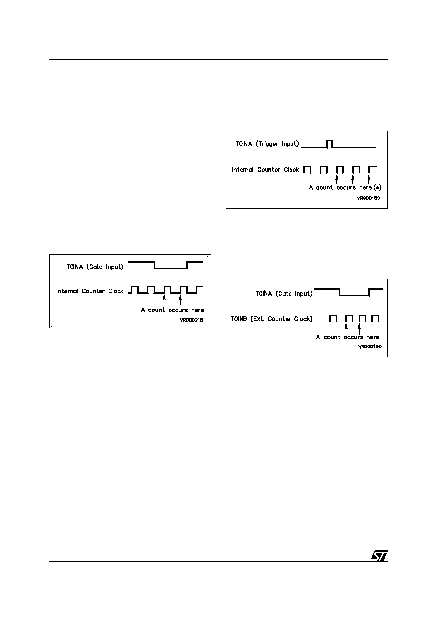
118/230
ST92163 - MULTIFUNCTION TIMER (MFT)
MULTIFUNCTION TIMER (Cont'd)
8.2.3.1 TxINA = I/O - TxINB = I/O
Input pins A and B are not used by the Timer. The
counter clock is internally generated and the up/
down selection may be made only by software via
the UDC (Software Up/Down) bit in the TCR regis-
ter.
8.2.3.2 TxINA = I/O - TxINB = Trigger
The signal applied to input pin B acts as a trigger
signal on REG1R register. The prescaler clock is
internally generated and the up/down selection
may be made only by software via the UDC (Soft-
ware Up/Down) bit in the TCR register.
8.2.3.3 TxINA = Gate - TxINB = I/O
The signal applied to input pin A acts as a gate sig-
nal for the internal clock (i.e. the counter runs only
when the gate signal is at a low level). The counter
clock is internally generated and the up/down con-
trol may be made only by software via the UDC
(Software Up/Down) bit in the TCR register.
8.2.3.4 TxINA = Gate - TxINB = Trigger
Both input pins A and B are connected to the timer,
with the resulting effect of combining the actions
relating to the previously described configurations.
8.2.3.5 TxINA = I/O - TxINB = Ext. Clock
The signal applied to input pin B is used as the ex-
ternal clock for the prescaler. The up/down selec-
tion may be made only by software via the UDC
(Software Up/Down) bit in the TCR register.
8.2.3.6 TxINA = Trigger - TxINB = I/O
The signal applied to input pin A acts as a trigger
for REG0R, initiating the action for which the reg-
ister was programmed (i.e. a reload or capture).
The prescaler clock is internally generated and the
up/down selection may be made only by software
via the UDC (Software Up/Down) bit in the TCR
register.
(*) The timer is in One shot mode and REGOR in
Reload mode
8.2.3.7 TxINA = Gate - TxINB = Ext. Clock
The signal applied to input pin B, gated by the sig-
nal applied to input pin A, acts as external clock for
the prescaler. The up/down control may be made
only by software action through the UDC bit in the
TCR register.
8.2.3.8 TxINA = Trigger - TxINB = Trigger
The signal applied to input pin A (or B) acts as trig-
ger signal for REG0R (or REG1R), initiating the
action for which the register has been pro-
grammed. The counter clock is internally generat-
ed and the up/down selection may be made only
by software via the UDC (Software Up/Down) bit in
the TCR register.
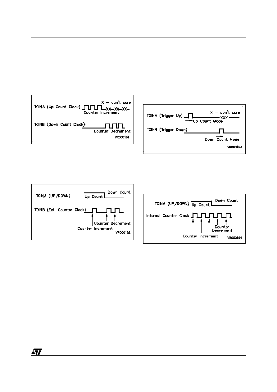
119/230
ST92163 - MULTIFUNCTION TIMER (MFT)
MULTIFUNCTION TIMER (Cont'd)
8.2.3.9 TxINA = Clock Up - TxINB = Clock Down
The edge received on input pin A (or B) performs a
one step up (or down) count, so that the counter
clock and the up/down control are external. Setting
the UDC bit in the TCR register has no effect in
this configuration, and input pin B has priority on
input pin A.
8.2.3.10 TxINA = Up/Down - TxINB = Ext Clock
An High (or Low) level applied to input pin A sets
the counter in the up (or down) count mode, while
the signal applied to input pin B is used as clock for
the prescaler. Setting the UDC bit in the TCR reg-
ister has no effect in this configuration.
8.2.3.11 TxINA = Trigger Up - TxINB = Trigger
Down
Up/down control is performed through both input
pins A and B. A edge on input pin A sets the up
count mode, while a edge on input pin B (which
has priority on input pin A) sets the down count
mode. The counter clock is internally generated,
and setting the UDC bit in the TCR register has no
effect in this configuration.
8.2.3.12 TxINA = Up/Down - TxINB = I/O
An High (or Low) level of the signal applied on in-
put pin A sets the counter in the up (or down) count
mode. The counter clock is internally generated.
Setting the UDC bit in the TCR register has no ef-
fect in this configuration.
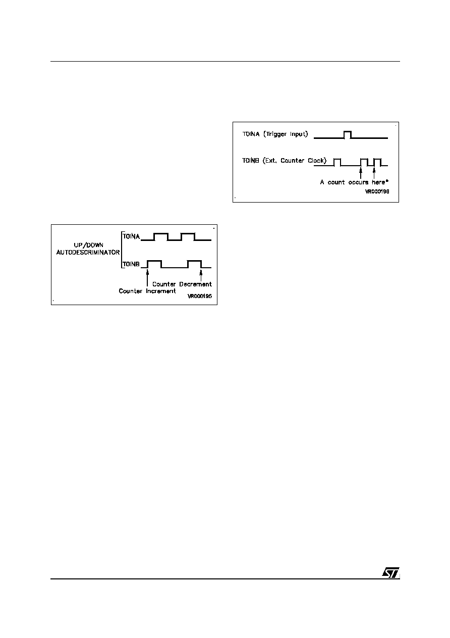
120/230
ST92163 - MULTIFUNCTION TIMER (MFT)
MULTIFUNCTION TIMER (Cont'd)
8.2.3.13 Autodiscrimination Mode
The phase between two pulses (respectively on in-
put pin B and input pin A) generates a one step up
(or down) count, so that the up/down control and
the counter clock are both external. Thus, if the ris-
ing edge of TxINB arrives when TxINA is at a low
level, the timer is incremented (no action if the ris-
ing edge of TxINB arrives when TxINA is at a high
level). If the falling edge of TxINB arrives when
TxINA is at a low level, the timer is decremented
(no action if the falling edge of TxINB arrives when
TxINA is at a high level).
Setting the UDC bit in the TCR register has no ef-
fect in this configuration.
8.2.3.14 TxINA = Trigger - TxINB = Ext. Clock
The signal applied to input pin A acts as a trigger
signal on REG0R, initiating the action for which the
register was programmed (i.e. a reload or cap-
ture), while the signal applied to input pin B is used
as the clock for the prescaler.
(*) The timer is in One shot mode and REG0R in
reload mode
8.2.3.15 TxINA = Ext. Clock - TxINB = Trigger
The signal applied to input pin B acts as a trigger,
performing a capture on REG1R, while the signal
applied to input pin A is used as the clock for the
prescaler.
8.2.3.16 TxINA = Trigger - TxINB = Gate
The signal applied to input pin A acts as a trigger
signal on REG0R, initiating the action for which the
register was programmed (i.e. a reload or cap-
ture), while the signal applied to input pin B acts as
a gate signal for the internal clock (i.e. the counter
runs only when the gate signal is at a low level).
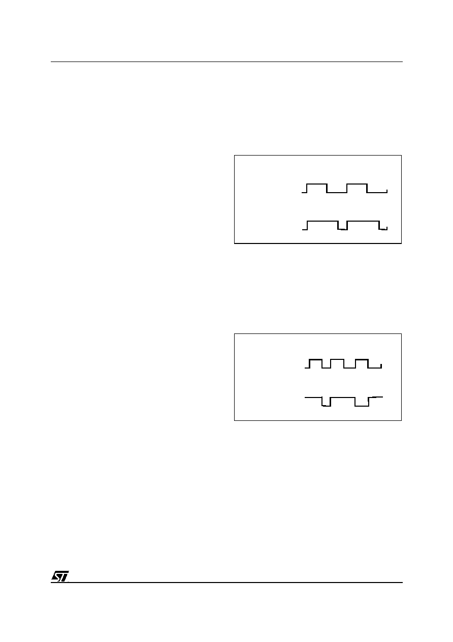
121/230
ST92163 - MULTIFUNCTION TIMER (MFT)
MULTIFUNCTION TIMER (Cont'd)
8.2.4 Output Pin Assignment
Two external outputs are available when pro-
grammed as Alternate Function Outputs of the I/O
pins.
Two registers Output A Control Register (OACR)
and Output B Control Register (OBCR) define the
driver for the outputs and the actions to be per-
formed.
Each of the two output pins can be driven from any
of the three possible sources:
≠ Compare Register 0 event logic
≠ Compare Register 1 event logic
≠ Overflow/Underflow event logic.
Each of these three sources can cause one of the
following four actions on any of the two outputs:
≠ Nop
≠ Set
≠ Reset
≠ Toggle
Furthermore an On Chip Event signal can be driv-
en by two of the three sources: the Over/Under-
flow event and Compare 0 event by programming
the CEV bit of the OACR register and the OEV bit
of OBCR register respectively. This signal can be
used internally to synchronise another on-chip pe-
ripheral.
Output Waveforms
Depending on the programming of OACR and OB-
CR, the following example waveforms can be gen-
erated on TxOUTA and TxOUTB pins.
For a configuration where TxOUTA is driven by the
Over/Underflow (OUF) and the Compare 0 event
(CM0), and TxOUTB is driven by the Over/Under-
flow and Compare 1 event (CM1):
OACR is programmed with TxOUTA preset to "0",
OUF sets TxOUTA, CM0 resets TxOUTA and
CM1 does not affect the output.
OBCR is programmed with TxOUTB preset to "0",
OUF sets TxOUTB, CM1 resets TxOUTB while
CM0 does not affect the output.
For a configuration where TxOUTA is driven by the
Over/Underflow, by Compare 0 and by Compare
1; TxOUTB is driven by both Compare 0 and Com-
pare 1. OACR is programmed with TxOUTA pre-
set to "0". OUF toggles Output 0, as do CM0 and
CM1. OBCR is programmed with TxOUTB preset
to "1". OUF does not affect the output; CM0 resets
TxOUTB and CM1 sets it.
OACR = [101100X0]
OBCR = [111000X0]
T0OUTA
T0OUTB
OUF
COMP1
OUF
COMP1
OUF COMP0 OUF COMP0
OACR = [010101X0]
OBCR = [100011X1]
T0OUTA
T0OUTB
COMP1 COMP1
OUF
OUF
COMP0
COMP0
COMP0
COMP0
COMP1 COMP1
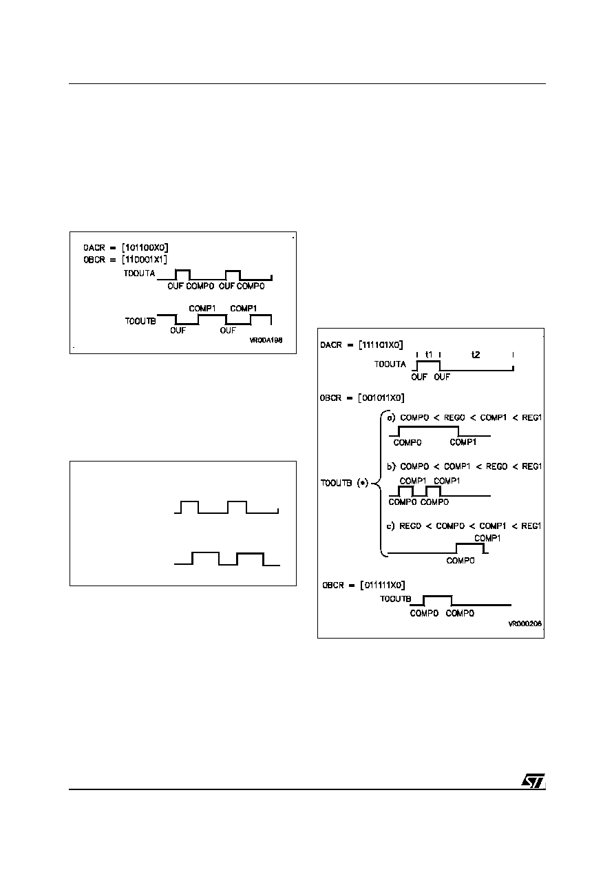
122/230
ST92163 - MULTIFUNCTION TIMER (MFT)
MULTIFUNCTION TIMER (Cont'd)
For a configuration where TxOUTA is driven by the
Over/Underflow and by Compare 0, and TxOUTB
is driven by the Over/Underflow and by Compare
1. OACR is programmed with TxOUTA preset to
"0". OUF sets TxOUTA while CM0 resets it, and
CM1 has no effect. OBCR is programmed with Tx-
OUTB preset to "1". OUF toggles TxOUTB, CM1
sets it and CM0 has no effect.
For a configuration where TxOUTA is driven by the
Over/Underflow and by Compare 0, and TxOUTB
is driven by Compare 0 and 1. OACR is pro-
grammed with TxOUTA preset to "0". OUF sets
TxOUTA, CM0 resets it and CM1 has no effect.
OBCR is programmed with TxOUTB preset to "0".
OUF has no effect, CM0 sets TxOUTB and CM1
toggles it.
Output Waveform Samples In Biload Mode
TxOUTA is programmed to monitor the two time
intervals, t1 and t2, of the Biload Mode, while Tx-
OUTB is independent of the Over/Underflow and
is driven by the different values of Compare 0 and
Compare 1. OACR is programmed with TxOUTA
preset to "0". OUF toggles the output and CM0 and
CM1 do not affect TxOUTA. OBCR is programmed
with TxOUTB preset to "0". OUF has no effect,
while CM1 resets TxOUTB and CM0 sets it.
Depending on the CM1/CM0 values, three differ-
ent sample waveforms have been drawn based on
the above mentioned configuration of OBCR. In
the last case, with a different programmed value of
OBCR, only Compare 0 drives TxOUTB, toggling
the output.
Note (*) Depending on the CMP1R/CMP0R values
OACR = [101100X0]
OBCR = [000111X0]
T0OUTA
T0OUTB
OUF
OUF
COMP0
COMP0
COMP0
COMP0
COMP1
COMP1

123/230
ST92163 - MULTIFUNCTION TIMER (MFT)
MULTIFUNCTION TIMER (Cont'd)
8.2.5 Interrupt and DMA
8.2.5.1 Timer Interrupt
The timer has 5 different Interrupt sources, be-
longing to 3 independent groups, which are as-
signed to the following Interrupt vectors:
Table 22. Timer Interrupt Structure
The three least significant bits of the vector pointer
address represent the relative priority assigned to
each group, where 000 represents the highest pri-
ority level. These relative priorities are fixed by
hardware, according to the source which gener-
ates the interrupt request. The 5 most significant
bits represent the general priority and are pro-
grammed by the user in the Interrupt Vector Reg-
ister (T_IVR).
Each source can be masked by a dedicated bit in
the Interrupt/DMA Mask Register (IDMR) of each
timer, as well as by a global mask enable bit (ID-
MR.7) which masks all interrupts.
If an interrupt request (CM0 or CP0) is present be-
fore the corresponding pending bit is reset, an
overrun condition occurs. This condition is flagged
in two dedicated overrun bits, relating to the
Comp0 and Capt0 sources, in the Timer Flag Reg-
ister (T_FLAGR).
8.2.5.2 Timer DMA
Two Independent DMA channels, associated with
Comp0 and Capt0 respectively, allow DMA trans-
fers from Register File or Memory to the Comp0
Register, and from the Capt0 Register to Register
File or Memory). If DMA is enabled, the Capt0 and
Comp0 interrupts are generated by the corre-
sponding DMA End of Block event. Their priority is
set by hardware as follows:
≠ Compare 0 Destination
--
Lower Priority
≠ Capture 0 Source
--
Higher Priority
The two DMA request sources are independently
maskable by the CP0D and CM0D DMA Mask bits
in the IDMR register.
The two DMA End of Block interrupts are inde-
pendently enabled by the CP0I and CM0I Interrupt
mask bits in the IDMR register.
8.2.5.3 DMA Pointers
The 6 programmable most significant bits of the
DMA Counter Pointer Register (DCPR) and of the
DMA Address Pointer Register (DAPR) are com-
mon to both channels (Comp0 and Capt0). The
Comp0 and Capt0 Address Pointers are mapped
as a pair in the Register File, as are the Comp0
and Capt0 DMA Counter pair.
In order to specify either the Capt0 or the Comp0
pointers, according to the channel being serviced,
the Timer resets address bit 1 for CAPT0 and sets
it for COMP0, when the D0 bit in the DCPR regis-
ter is equal to zero (Word address in Register
File). In this case (transfers between peripheral
registers and memory), the pointers are split into
two groups of adjacent Address and Counter pairs
respectively.
For peripheral register to register transfers (select-
ed by programming "1" into bit 0 of the DCPR reg-
ister), only one pair of pointers is required, and the
pointers are mapped into one group of adjacent
positions.
The DMA Address Pointer Register (DAPR) is not
used in this case, but must be considered re-
served.
Figure 70. Pointer Mapping for Transfers
between Registers and Memory
Interrupt Source
Vector Address
COMP 0
COMP 1
xxxx x110
CAPT 0
CAPT 1
xxxx x100
Overflow/Underflow
xxxx x000
Register File
Address
Pointers
Comp0 16 bit
Addr Pointer
YYYYYY11(l)
YYYYYY10(h)
Capt0 16 bit
Addr Pointer
YYYYYY01(l)
YYYYYY00(h)
DMA
Counters
Comp0 DMA
16 bit Counter
XXXXXX11(l)
XXXXXX10(h)
Capt0 DMA
16 bit Counter
XXXXXX01(l)
XXXXXX00(h)

124/230
ST92163 - MULTIFUNCTION TIMER (MFT)
MULTIFUNCTION TIMER (Cont'd)
Figure 71. Pointer Mapping for Register to
Register Transfers
8.2.5.4 DMA Transaction Priorities
Each Timer DMA transaction is a 16-bit operation,
therefore two bytes must be transferred sequen-
tially, by means of two DMA transfers. In order to
speed up each word transfer, the second byte
transfer is executed by automatically forcing the
peripheral priority to the highest level (000), re-
gardless of the previously set level. It is then re-
stored to its original value after executing the
transfer. Thus, once a request is being serviced,
its hardware priority is kept at the highest level re-
gardless of the other Timer internal sources, i.e.
once a Comp0 request is being serviced, it main-
tains a higher priority, even if a Capt0 request oc-
curs between the two byte transfers.
8.2.5.5 DMA Swap Mode
After a complete data table transfer, the transac-
tion counter is reset and an End Of Block (EOB)
condition occurs, the block transfer is completed.
The End Of Block Interrupt routine must at this
point reload both address and counter pointers of
the channel referred to by the End Of Block inter-
rupt source, if the application requires a continu-
ous high speed data flow. This procedure causes
speed limitations because of the time required for
the reload routine.
The SWAP feature overcomes this drawback, al-
lowing high speed continuous transfers. Bit 2 of
the DMA Counter Pointer Register (DCPR) and of
the DMA Address Pointer Register (DAPR), tog-
gles after every End Of Block condition, alternately
providing odd and even address (D2-D7) for the
pair of pointers, thus pointing to an updated pair,
after a block has been completely transferred. This
allows the User to update or read the first block
and to update the pointer values while the second
is being transferred. These two toggle bits are soft-
ware writable and readable, mapped in DCPR bit 2
for the CM0 channel, and in DAPR bit 2 for the
CP0 channel (though a DMA event on a channel,
in Swap mode, modifies a field in DAPR and
DCPR common to both channels, the DAPR/
DCPR content used in the transfer is always the bit
related to the correct channel).
SWAP mode can be enabled by the SWEN bit in
the IDCR Register.
WARNING
:
Enabling SWAP mode affects both
channels (CM0 and CP0).
Register File
8 bit Counter
XXXXXX11
Compare 0
8 bit Addr Pointer
XXXXXX10
8 bit Counter
XXXXXX01
Capture 0
8 bit Addr Pointer
XXXXXX00

125/230
ST92163 - MULTIFUNCTION TIMER (MFT)
MULTIFUNCTION TIMER (Cont'd)
8.2.5.6 DMA End Of Block Interrupt Routine
An interrupt request is generated after each block
transfer (EOB) and its priority is the same as that
assigned in the usual interrupt request, for the two
channels. As a consequence, they will be serviced
only when no DMA request occurs, and will be
subject to a possible OUF Interrupt request, which
has higher priority.
The following is a typical EOB procedure (with
swap mode enabled):
≠ Test Toggle bit and Jump.
≠ Reload Pointers (odd or even depending on tog-
gle bit status).
≠ Reset EOB bit: this bit must be reset only after
the old pair of pointers has been restored, so
that, if a new EOB condition occurs, the next pair
of pointers is ready for swapping.
≠ Verify the software protection condition (see
Section 0.1.5.7
).
≠ Read the corresponding Overrun bit: this con-
firms that no DMA request has been lost in the
meantime.
≠ Reset the corresponding pending bit.
≠ Reenable DMA with the corresponding DMA
mask bit (must always be done after resetting
the pending bit)
≠ Return.
WARNING: The EOB bits are read/write only for
test purposes. Writing a logical "1" by software
(when the SWEN bit is set) will cause a spurious
interrupt request. These bits are normally only re-
set by software.
8.2.5.7 DMA Software Protection
A second EOB condition may occur before the first
EOB routine is completed, this would cause a not
yet updated pointer pair to be addressed, with con-
sequent overwriting of memory. To prevent these
errors, a protection mechanism is provided, such
that the attempted setting of the EOB bit before it
has been reset by software will cause the DMA
mask on that channel to be reset (DMA disabled),
thus blocking any further DMA operation. As
shown above, this mask bit should always be
checked in each EOB routine, to ensure that all
DMA transfers are properly served.
8.2.6 Register Description
Note: In the register description on the following
pages, register and page numbers are given using
the example of Timer 0. On devices with more
than one timer, refer to the device register map for
the adresses and page numbers.
126/230
ST92163 - MULTIFUNCTION TIMER (MFT)
MULTIFUNCTION TIMER (Cont'd)
CAPTURE LOAD 0 HIGH REGISTER (REG0HR)
R240 - Read/Write
Register Page: 10
Reset value: undefined
This register is used to capture values from the
Up/Down counter or load preset values (MSB).
CAPTURE LOAD 0 LOW REGISTER (REG0LR)
R241 - Read/Write
Register Page: 10
Reset value: undefined
This register is used to capture values from the
Up/Down counter or load preset values (LSB).
CAPTURE LOAD 1 HIGH REGISTER (REG1HR)
R242 - Read/Write
Register Page: 10
Reset value: undefined
This register is used to capture values from the
Up/Down counter or load preset values (MSB).
CAPTURE LOAD 1 LOW REGISTER (REG1LR)
R243 - Read/Write
Register Page: 10
Reset value: undefined
This register is used to capture values from the
Up/Down counter or load preset values (LSB).
COMPARE 0 HIGH REGISTER (CMP0HR)
R244 - Read/Write
Register Page: 10
Reset value: 0000 0000 (00h)
This register is used to store the MSB of the 16-bit
value to be compared to the Up/Down counter
content.
COMPARE 0 LOW REGISTER (CMP0LR)
R245 - Read/Write
Register Page: 10
Reset value: 0000 0000 (00h)
This register is used to store the LSB of the 16-bit
value to be compared to the Up/Down counter
content.
COMPARE 1 HIGH REGISTER (CMP1HR)
R246 - Read/Write
Register Page: 10
Reset value: 0000 0000 (00h)
This register is used to store the MSB of the 16-bit
value to be compared to the Up/Down counter
content.
COMPARE 1 LOW REGISTER (CMP1LR)
R247 - Read/Write
Register Page: 10
Reset value: 0000 0000 (00h)
This register is used to store the LSB of the 16-bit
value to be compared to the Up/Down counter
content.
7
0
R15
R14
R13
R12
R11
R10
R9
R8
7
0
R7
R6
R5
R4
R3
R2
R1
R0
7
0
R15
R14
R13
R12
R11
R10
R9
R8
7
0
R7
R6
R5
R4
R3
R2
R1
R0
7
0
R15
R14
R13
R12
R11
R10
R9
R8
7
0
R7
R6
R5
R4
R3
R2
R1
R0
7
0
R15
R14
R13
R12
R11
R10
R9
R8
7
0
R7
R6
R5
R4
R3
R2
R1
R0

127/230
ST92163 - MULTIFUNCTION TIMER (MFT)
MULTIFUNCTION TIMER (Cont'd)
TIMER CONTROL REGISTER (TCR)
R248 - Read/Write
Register Page: 10
Reset value: 0000 0000 (00h)
Bit 7 = CEN:
Counter enable
.
This bit is ANDed with the Global Counter Enable
bit (GCEN) in the CICR register (R230). The
GCEN bit is set after the Reset cycle.
0: Stop the counter and prescaler
1: Start the counter and prescaler (without reload).
Note: Even if CEN=0, capture and loading will
take place on a trigger event.
Bit 6 = CCP0:
Clear on capture
.
0: No effect
1: Clear the counter and reload the prescaler on a
REG0R or REG1R capture event
Bit 5 = CCMP0:
Clear on Compare
.
0: No effect
1: Clear the counter and reload the prescaler on a
CMP0R compare event
Bit 4 = CCL:
Counter clear
.
This bit is reset by hardware after being set by
software (this bit always returns "0" when read).
0: No effect
1: Clear the counter without generating an inter-
rupt request
Bit 3 = UDC:
Up/Down software selection
.
If the direction of the counter is not fixed by hard-
ware (TxINA and/or TxINB pins, see par. 10.3) it
can be controlled by software using the UDC bit.
0: Down counting
1: Up counting
Bit 2 = UDCS:
Up/Down count status
.
This bit is read only and indicates the direction of
the counter.
0: Down counting
1: Up counting
Bit 1 = OF0:
OVF/UNF state
.
This bit is read only.
0: No overflow or underflow occurred
1: Overflow or underflow occurred during a Cap-
ture on Register 0
Bit 0 = CS
Counter Status
.
This bit is read only and indicates the status of the
counter.
0: Counter halted
1: Counter running
7
0
CEN
CCP
0
CCMP
0
CCL
UDC
UDC
S
OF0
CS
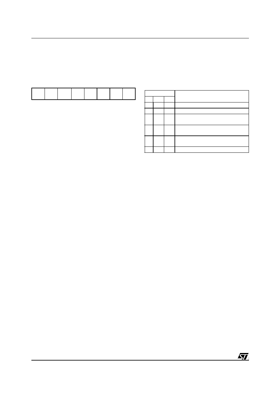
128/230
ST92163 - MULTIFUNCTION TIMER (MFT)
MULTIFUNCTION TIMER (Cont'd)
TIMER MODE REGISTER (TMR)
R249 - Read/Write
Register Page: 10
Reset value: 0000 0000 (00h)
Bit 7 = OE1:
Output 1 enable.
0: Disable the Output 1 (TxOUTB pin) and force it
high.
1: Enable the Output 1 (TxOUTB pin)
The relevant I/O bit must also be set to Alternate
Function
Bit 6 = OE0:
Output 0 enable.
0: Disable the Output 0 (TxOUTA pin) and force it
high
1: Enable the Output 0 (TxOUTA pin).
The relevant I/O bit must also be set to Alternate
Function
Bit 5 = BM:
Bivalu
e
mode
.
This bit works together with the RM1 and RM0 bits
to select the timer operating mode (see
Table 4
).
0: Disable bivalue mode
1: Enable bivalue mode
Bit 4 = RM1:
REG1R mode
.
This bit works together with the BM and RM0 bits
to select the timer operating mode. Refer to
Table
4
.
Note: This bit has no effect when the Bivalue
Mode is enabled (BM=1).
Bit 3 = RM0:
REG0R mode
.
This bit works together with the BM and RM1 bits
to select the timer operating mode. Refer to
Table
4
.
Table 23. Timer Operating Modes
Bit 2 = ECK
Timer clock control
.
0: The prescaler clock source is selected depend-
ing on the IN0 - IN3 bits in the T_ICR register
1: Enter Parallel mode (for Timer 1 and Timer 3
only, no effect for Timer 0 and 2). See
Section
0.1.2.12
.
Bit 1 = REN:
Retrigger mode
.
0: Enable retriggerable mode
1: Disable retriggerable mode
Bit 0 = CO:
Continous/One shot mode
.
0: Continuous mode (with autoreload on End of
Count condition)
1: One shot mode
7
0
OE1
OE0
BM
RM1
RM0
ECK
REN
C0
TMR Bits
Timer Operating Modes
BM RM1 RM0
1
x
0
Biload mode
1
x
1
Bicapture mode
0
0
0
Load from REG0R and Monitor on
REG1R
0
1
0
Load from REG0R and Capture on
REG1R
0
0
1
Capture on REG0R and Monitor on
REG1R
0
1
1
Capture on REG0R and REG1R
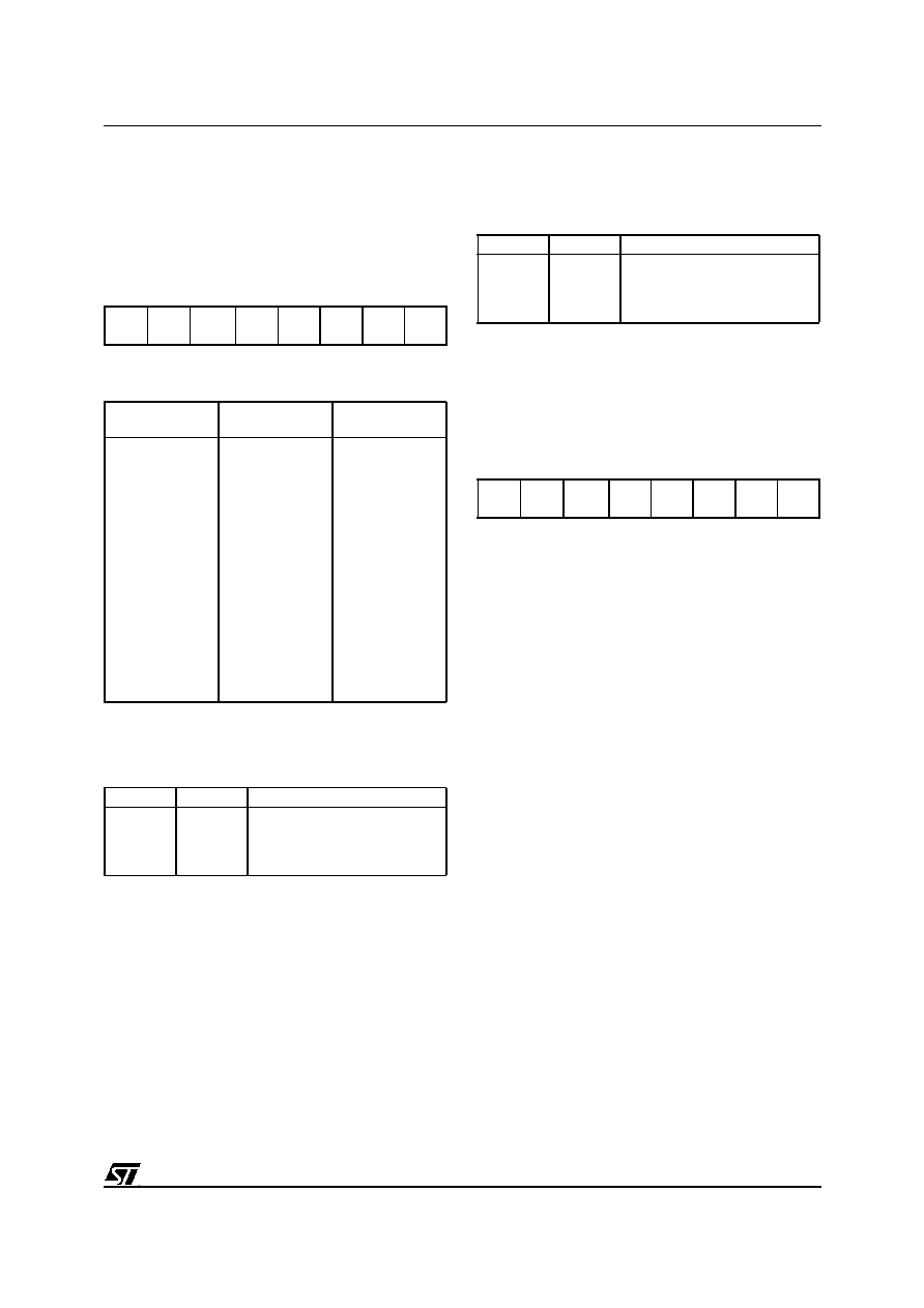
129/230
ST92163 - MULTIFUNCTION TIMER (MFT)
MULTIFUNCTION TIMER (Cont'd)
EXTERNAL INPUT CONTROL REGISTER
(T_ICR)
R250 - Read/Write
Register Page: 10
Reset value: 0000 0000 (00h)
Bits 7:4 = IN[3:0]:
Input pin function.
These bits are set and cleared by software.
Bits 3:2 = A[0:1]:
TxINA Pin event
.
These bits are set and cleared by software.
Bits 1:0 = B[0:1]:
TxINB Pin event
.
These bits are set and cleared by software.
PRESCALER REGISTER (PRSR)
R251 - Read/Write
Register Page: 10
Reset value: 0000 0000 (00h)
This register holds the preset value for the 8-bit
prescaler. The PRSR content may be modified at
any time, but it will be loaded into the prescaler at
the following prescaler underflow, or as a conse-
quence of a counter reload (either by software or
upon external request).
Following a RESET condition, the prescaler is au-
tomatically loaded with 00h, so that the prescaler
divides by 1 and the maximum counter clock is
generated (Crystal oscillator clock frequency divid-
ed by 6 when MODER.5 = DIV2 bit is set).
The binary value programmed in the PRSR regis-
ter is equal to the divider value minus one. For ex-
ample, loading PRSR with 24 causes the prescal-
er to divide by 25.
7
0
IN3
IN2
IN1
IN0
A0
A1
B0
B1
IN[3:0] bits
TxINA
Pin Function
TxINB Input
Pin Function
0000
0001
0010
0011
0100
0101
0110
0111
1000
1001
1010
1011
1100
1101
1110
1111
not used
not used
Gate
Gate
not used
Trigger
Gate
Trigger
Clock Up
Up/Down
Trigger Up
Up/Down
Autodiscr.
Trigger
Ext. Clock
Trigger
not used
Trigger
not used
Trigger
Ext. Clock
not used
Ext. Clock
Trigger
Clock Down
Ext. Clock
Trigger Down
not used
Autodiscr.
Ext. Clock
Trigger
Gate
A0
A1
TxINA Pin Event
0
0
1
1
0
1
0
1
No operation
Falling edge sensitive
Rising edge sensitive
Rising and falling edges
B0
B1
TxINB Pin Event
0
0
1
1
0
1
0
1
No operation
Falling edge sensitive
Rising edge sensitive
Rising and falling edges
7
0
P7
P6
P5
P4
P3
P2
P1
P0

130/230
ST92163 - MULTIFUNCTION TIMER (MFT)
MULTIFUNCTION TIMER (Cont'd)
OUTPUT A CONTROL REGISTER (OACR)
R252 - Read/Write
Register Page: 10
Reset value: 0000 0000
Bits 7:6 = C0E[0:1]:
COMP0
action bits
.
These bits are set and cleared by software. They
configure the action to be performed on the Tx-
OUTA pin when a successful compare of the
CMP0R register occurs. Refer to
Table 5
for the
list of actions that can be configured.
Bits 5:4 = C1E[0:1]:
COMP1 action bits
.
These bits are set and cleared by software. They
configure the action to be performed on the Tx-
OUTA pin when a successful compare of the
CMP1R register occurs. Refer to
Table 5
for the
list of actions that can be configured.
Bits 3:2 = OUE[0:1]:
OVF/UNF action bits
.
These bits are set and cleared by software. They
configure the action to be performed on the Tx-
OUTA pin when an Overflow or Underflow of the
U/D counter occurs. Refer to
Table 5
for the list of
actions that can be configured.
Table 24. Output A Action Bits
Notes:
≠ xx stands for C0, C1 or OU.
≠ Whenever more than one event occurs simulta-
neously, Action bit 0 will be the result of ANDing
Action bit 0 of all simultaneous events and Action
bit 1 will be the result of ANDing Action bit 1 of all
simultaneous events.
Bit 1 = CEV:
On-Chip event on CMP0R
.
This bit is set and cleared by software.
0: No action
1: A successful compare on CMP0R activates the
on-chip event signal (a single pulse is generat-
ed)
Bit 0 = OP:
TxOUTA preset value
.
This bit is set and cleared by software and by hard-
ware. The value of this bit is the preset value of the
TxOUTA pin. Reading this bit returns the current
state of the TxOUTA pin (useful when it is selected
in toggle mode).
7
0
C0E0 C0E1 C1E0 C1E1 OUE0 OUE1 CEV 0P
xxE0
xxE1
Action on TxOUTA pin when an xx
event occurs
0
0
Set
0
1
Toggle
1
0
Reset
1
1
NOP

131/230
ST92163 - MULTIFUNCTION TIMER (MFT)
MULTIFUNCTION TIMER (Cont'd)
OUTPUT B CONTROL REGISTER (OBCR)
R253 - Read/Write
Register Page: 10
Reset value: 0000 0000 (00h)
Bits 7:6 = C0E[0:1]:
COMP0
Action Bits
.
These bits are set and cleared by software. They
configure the type of action to be performed on the
TxOUTB output pin when successful compare of
the CMP0R register occurs. Refer to
Table 6
for
the list of actions that can be configured.
Bits 5:4 = C0E[0:1]:
COMP1 Action Bits
.
These bits are set and cleared by software. They
configure the type of action to be performed on the
TxOUTB output pin when a successful compare of
the CMP1R register occurs. Refer to
Table 6
for
the list of actions that can be configured.
Bits 3:2 = OUE[0:1]:
OVF/UNF Action Bits
.
These bits are set and cleared by software.They
configure the type of action to be performed on the
TxOUTB output pin when an Overflow or Under-
flow on the U/D counter occurs. Refer to
Table 6
for the list of actions that can be configured.
Table 25. Output B Action Bits
Notes:
≠ xx stands for C0, C1 or OU.
≠ Whenever more than one event occurs simulta-
neously, Action Bit 0 will be the result of ANDing
Action Bit 0 of all simultaneous events and Action
Bit 1 will be the result of ANDing Action Bit 1 of
all simultaneous events.
Bit 1 = OEV:
On-Chip event on OVF/UNF
.
This bit is set and cleared by software.
0: No action
1: An underflow/overflow activates the on-chip
event signal (a single pulse is generated)
Bit 0 = OP:
TxOUTB preset value
.
This bit is set and cleared by software and by hard-
ware. The value of this bit is the preset value of the
TxOUTB pin. Reading this bit returns the current
state of the TxOUTB pin (useful when it is selected
in toggle mode).
7
0
C0E0 C0E1 C1E0 C1E1 OUE0 OUE1 OEV 0P
xxE0
xxE1
Action on the TxOUTB pin when an
xx event occurs
0
0
Set
0
1
Toggle
1
0
Reset
1
1
NOP

132/230
ST92163 - MULTIFUNCTION TIMER (MFT)
MULTIFUNCTION TIMER (Cont'd)
FLAG REGISTER (T_FLAGR)
R254 - Read/Write
Register Page: 10
Reset value: 0000 0000 (00h)
Bit
7 = CP0:
Capture 0 flag.
This bit is set by hardware after a capture on
REG0R register. An interrupt is generated de-
pending on the value of the GTIEN, CP0I bits in
the IDMR register and the A0 bit in the T_FLAGR
register. The CP0 bit must be cleared by software.
Setting by software acts as a software load/cap-
ture to/from the REG0R register.
0: No Capture 0 event
1: Capture 0 event occurred
Bit 6 = CP1:
Capture 1 flag
.
This bit is set by hardware after a capture on
REG1R register. An interrupt is generated de-
pending on the value of the GTIEN, CP0I bits in
the IDMR register and the A0 bit in the T_FLAGR
register. The CP1 bit must be cleared by software.
Setting by software acts as a capture event on the
REG1R register, except when in Bicapture mode.
0: No Capture 1 event
1: Capture 1 event occurred
Bit 5 = CM0:
Compare 0 flag
.
This bit is set by hardware after a successful com-
pare on the CMP0R register. An interrupt is gener-
ated if the GTIEN and CM0I bits in the IDMR reg-
ister are set. The CM0 bit is cleared by software.
0: No Compare 0 event
1: Compare 0 event occurred
Bit 4 = CM1:
Compare 1 flag.
This bit is set after a successful compare on
CMP1R register. An interrupt is generated if the
GTIEN and CM1I bits in the IDMR register are set.
The CM1 bit is cleared by software.
0: No Compare 1 event
1: Compare 1 event occurred
Bit 3 = OUF:
Overflow/Underflow
.
This bit is set by hardware after a counter Over/
Underflow condition. An interrupt is generated if
GTIEN and OUI=1 in the IDMR register. The OUF
bit is cleared by software.
0: No counter overflow/underflow
1: Counter overflow/underflow
Bit 2 = OCP0:
Overrun on Capture 0.
This bit is set by hardware when more than one
INT/DMA requests occur before the CP0 flag is
cleared by software or whenever a capture is sim-
ulated by setting the CP0 flag by software. The
OCP0 flag is cleared by software.
0: No capture 0 overrun
1: Capture 0 overrun
Bit 1 = OCM0:
Overrun on compare 0.
This bit is set by hardware when more than one
INT/DMA requests occur before the CM0 flag is
cleared by software.The OCM0 flag is cleared by
software.
0: No compare 0 overrun
1: Compare 0 overrun
Bit 0 = A0:
Capture interrupt function
.
This bit is set and cleared by software.
0: Configure the capture interrupt as an OR func-
tion of REG0R/REG1R captures
1: Configure the capture interrupt as an AND func-
tion of REG0R/REG1R captures
Note: When A0 is set, both CP0I and CP1I in the
IDMR register must be set to enable both capture
interrupts.
7
0
CP0
CP1
CM0
CM1
OUF
OCP
0
OCM
0
A0

133/230
ST92163 - MULTIFUNCTION TIMER (MFT)
MULTIFUNCTION TIMER (Cont'd)
INTERRUPT/DMA MASK REGISTER (IDMR)
R255 - Read/Write
Register Page: 10
Reset value: 0000 0000 (00h)
Bit
7 = GTIEN:
Global timer interrupt enable
.
This bit is set and cleared by software.
0: Disable all Timer interrupts
1: Enable all timer Timer Interrupts from enabled
sources
Bit 6 = CP0D:
Capture 0 DMA mask.
This bit is set by software to enable a Capt0 DMA
transfer and cleared by hardware at the end of the
block transfer.
0: Disable capture on REG0R DMA
1: Enable capture on REG0R DMA
Bit 5 = CP0I:
Capture 0 interrupt mask
.
0: Disable capture on REG0R interrupt
1: Enable capture on REG0R interrupt (or Capt0
DMA End of Block interrupt if CP0D=1)
Bit 4 = CP1I:
Capture 1 interrupt mask
.
This bit is set and cleared by software.
0: Disable capture on REG1R interrupt
1: Enable capture on REG1R interrupt
Bit 3 = CM0D:
Compare 0 DMA mask.
This bit is set by software to enable a Comp0 DMA
transfer and cleared by hardware at the end of the
block transfer.
0: Disable compare on CMP0R DMA
1: Enable compare on CMP0R DMA
Bit 2 = CM0I:
Compare 0 Interrupt mask
.
This bit is set and cleared by software.
0: Disable compare on CMP0R interrupt
1: Enable compare on CMP0R interrupt (or
Comp0 DMA End of Block interrupt if CM0D=1)
Bit 1 = CM1I:
Compare 1 Interrupt mask
.
This bit is set and cleared by software.
0: Disable compare on CMP1R interrupt
1: Enable compare on CMP1R interrupt
Bit 0 = OUI:
Overflow/Underflow interrupt mask
.
This bit is set and cleared by software.
0: Disable Overflow/Underflow interrupt
1: Enable Overflow/Underflow interrupt
DMA COUNTER POINTER REGISTER (DCPR)
R240 - Read/Write
Register Page: 9
Reset value: undefined
Bits
7:2 = DCP[7:2]:
MSBs of DMA counter regis-
ter address.
These are the most significant bits of the DMA
counter register address programmable by soft-
ware. The DCP2 bit may also be toggled by hard-
ware if the Timer DMA section for the Compare 0
channel is configured in Swap mode.
Bit 1 = DMA-SRCE:
DMA source selection.
This bit is set and cleared by hardware.
0: DMA source is a Capture on REG0R register
1: DMA destination is a Compare on CMP0R reg-
ister
Bit 0 = REG/MEM:
DMA area selection
.
This bit is set and cleared by software. It selects
the source and destination of the DMA area
0: DMA from/to memory
1: DMA from/to Register File
7
0
GT-
IEN
CP0D CP0I
CP1I
CM0
D
CM0I CM1I
OUI
7
0
DCP7 DCP6 DCP5 DCP4 DCP3 DCP2
DMA
SRCE
REG/
MEM
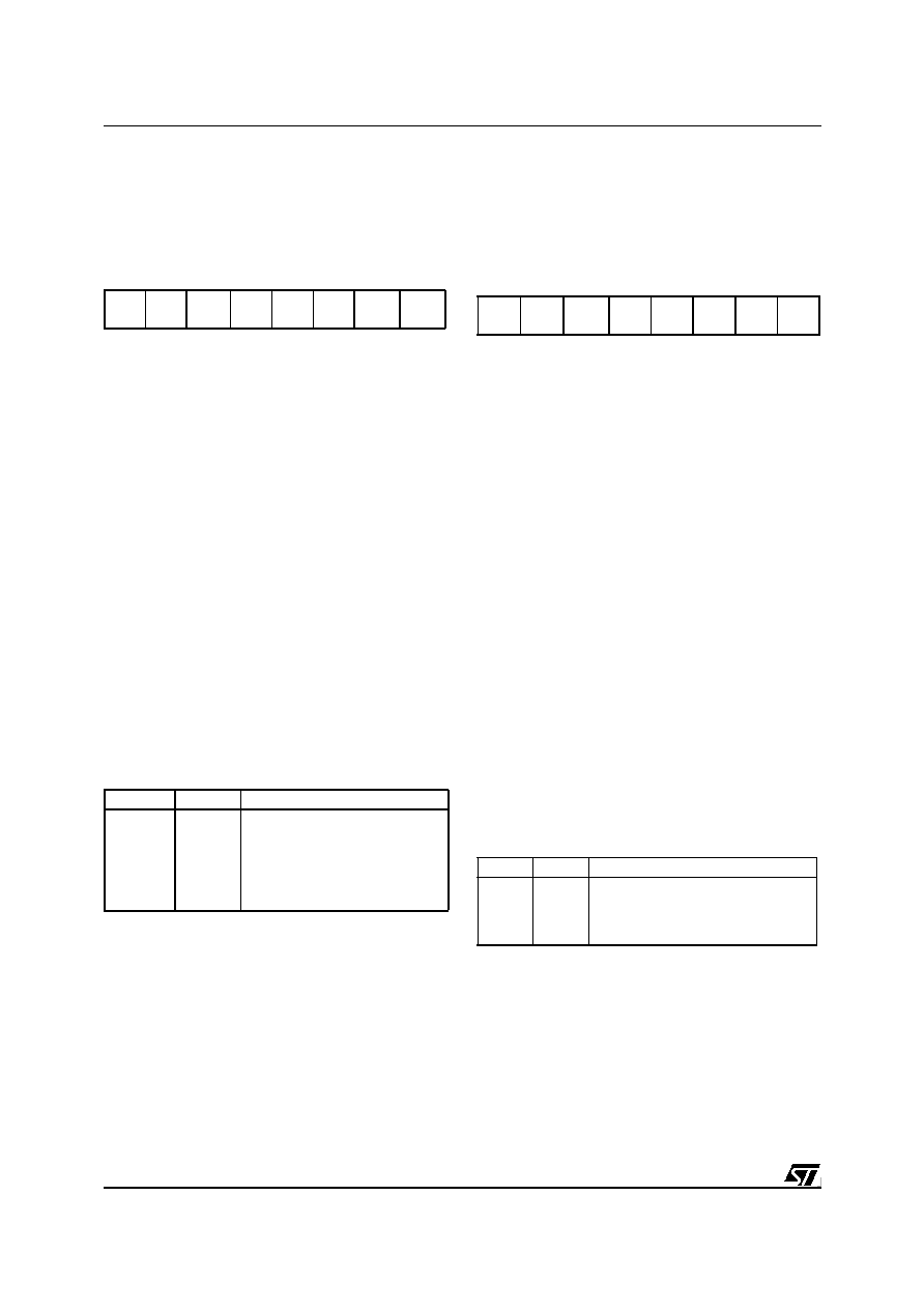
134/230
ST92163 - MULTIFUNCTION TIMER (MFT)
MULTIFUNCTION TIMER (Cont'd)
DMA ADDRESS POINTER REGISTER (DAPR)
R241 - Read/Write
Register Page: 9
Reset value: undefined
Bits
7:2 = DAP[7:2]:
MSB of DMA address regis-
ter location.
These are the most significant bits of the DMA ad-
dress register location programmable by software.
The DAP2 bit may also be toggled by hardware if
the Timer DMA section for the Compare 0 channel
is configured in Swap mode.
Note: During a DMA transfer with the Register
File, the DAPR is not used; however, in Swap
mode, DAP2 is used to point to the correct table.
Bit 1 = DMA-SRCE:
DMA source selection.
This bit is fixed by hardware.
0: DMA source is a Capture on REG0R register
1: DMA destination is a Compare on the CMP0R
register
Bit 0 = PRG/DAT:
DMA memory selection
.
This bit is set and cleared by software. It is only
meaningful if DCPR.REG/MEM=0.
0: The ISR register is used to extend the address
of data transferred by DMA (see MMU chapter).
1: The DMASR register is used to extend the ad-
dress of data transferred by DMA (see MMU
chapter).
INTERRUPT VECTOR REGISTER (T_IVR)
R242 - Read/Write
Register Page: 9
Reset value: xxxx xxx0
This register is used as a vector, pointing to the
16-bit interrupt vectors in memory which contain
the starting addresses of the three interrupt sub-
routines managed by each timer.
Only one Interrupt Vector Register is available for
each timer, and it is able to manage three interrupt
groups, because the 3 least significant bits are
fixed by hardware depending on the group which
generated the interrupt request.
In order to determine which request generated the
interrupt within a group, the T_FLAGR register can
be used to check the relevant interrupt source.
Bits
7:3 = V[4:0]:
MSB of the vector address.
These bits are user programmable and contain the
five most significant bits of the Timer interrupt vec-
tor addresses in memory. In any case, an 8-bit ad-
dress can be used to indicate the Timer interrupt
vector locations, because they are within the first
256 memory locations (see Interrupt and DMA
chapters).
Bits 2:1 = W[1:0]:
Vector address bits.
These bits are equivalent to bit 1 and bit 2 of the
Timer interrupt vector addresses in memory. They
are fixed by hardware, depending on the group of
sources which generated the interrupt request as
follows:.
Bit 0 = This bit is forced by hardware to 0.
7
0
DAP
7
DAP
6
DAP5 DAP4 DAP3 DAP2
DMA
SRCE
PRG
/DAT
REG/MEM PRG/DAT
DMA Source/Destination
0
0
1
1
0
1
0
1
ISR register used to address
memory
DMASR
register used to address
memory
Register file
Register file
7
0
V4
V3
V2
V1
V0
W1
W0
0
W1
W0
Interrupt Source
0
0
1
1
0
1
0
1
Overflow/Underflow even interrupt
Not available
Capture event interrupt
Compare event interrupt

135/230
ST92163 - MULTIFUNCTION TIMER (MFT)
MULTIFUNCTION TIMER (Cont'd)
INTERRUPT/DMA CONTROL REGISTER
(IDCR)
R243 - Read/Write
Register Page: 9
Reset value: 1100 0111 (C7h)
Bit 7 = CPE:
Capture 0 EOB
.
This bit is set by hardware when the End Of Block
condition is reached during a Capture 0 DMA op-
eration with the Swap mode enabled. When Swap
mode is disabled (SWEN bit = "0"), the CPE bit is
forced to 1 by hardware.
0: No end of block condition
1: Capture 0 End of block
Bit 6 = CME:
Compare 0 EOB
.
This bit is set by hardware when the End Of Block
condition is reached during a Compare 0 DMA op-
eration with the Swap mode enabled. When the
Swap mode is disabled (SWEN bit = "0"), the CME
bit is forced to 1 by hardware.
0: No end of block condition
1: Compare 0 End of block
Bit 5 = DCTS:
DMA capture transfer source
.
This bit is set and cleared by software. It selects
the source of the DMA operation related to the
channel associated with the Capture 0.
Note: The I/O port source is available only on spe-
cific devices.
0: REG0R register
1: I/O port.
Bit 4 = DCTD:
DMA compare transfer destination
.
This bit is set and cleared by software. It selects
the destination of the DMA operation related to the
channel associated with Compare 0.
Note: The I/O port destination is available only on
specific devices.
0: CMP0R register
1: I/O port
Bit 3 = SWEN:
Swap function enable
.
This bit is set and cleared by software.
0: Disable Swap mode
1: Enable Swap mode for both DMA channels.
Bits 2:0 = PL[2:0]:
Interrupt/DMA priority level
.
With these three bits it is possible to select the In-
terrupt and DMA priority level of each timer, as one
of eight levels (see Interrupt/DMA chapter).
I/O CONNECTION REGISTER (IOCR)
R248 - Read/Write
Register Page: 9
Reset value: 1111 1100 (FCh)
Bits
7:2 = not used.
Bit 1 = SC1:
Select connection odd.
This bit is set and cleared by software. It selects if
the TxOUTA and TxINA pins for Timer 1 and Timer
3 are connected on-chip or not.
0: T1OUTA / T1INA and T3OUTA/ T3INA uncon-
nected
1: T1OUTA connected internally to T1INA and
T3OUTA connected internally to T3INA
Bit 0 = SC0:
Select connection even.
This bit is set and cleared by software. It selects if
the TxOUTA and TxINA pins for Timer 0 and Timer
2 are connected on-chip or not.
0: T0OUTA / T0INA and T2OUTA/ T2INA uncon-
nected
1: T0OUTA connected internally to T0INA and
T2OUTA connected internally to T2INA
Note: Timer 1 and 2 are available only on some
devices. Refer to the device block diagram and
register map.
7
0
CPE
CME DCTS
DCT
D
SWE
N
PL2
PL1
PL0
7
0
SC1
SC0
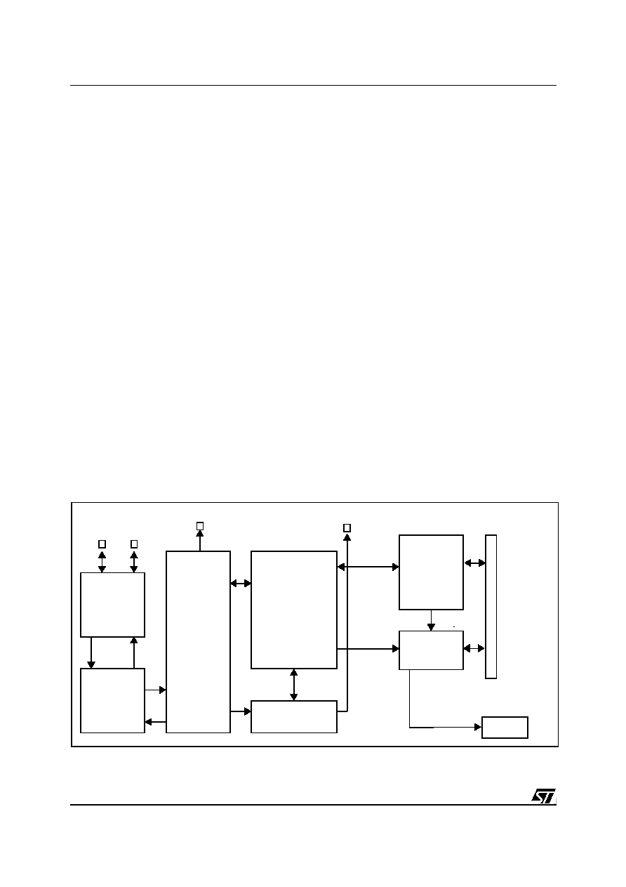
136/230
ST92163 - USB PERIPHERAL (USB)
8.3 USB PERIPHERAL (USB)
8.3.1 Introduction
The USB Peripheral provides a full-speed function
interface between the USB bus and the ST9 mi-
crocontroller.
8.3.2 Main Features
s
USB Specification Version 1.1 Compliant
s
Supports 8 device addresses
s
16 software configurable endpoints supporting:
∑
All USB transfer types (control, interrupt, bulk, and
isochronous)
∑
Burst-DMA transfers to up to 1K bytes RAM buffers
s
USB Suspend/Resume operations
s
On-Chip 3.3V Regulator
s
On-Chip USB Transceiver
s
Special functions on alternate output pins:
∑
USB upstream port Output Enable signal (USBOE)
∑
Start-Of-Frame pulse (SOFP)
s
Two bit-mirror registers
8.3.3 Functional Description
The USB interface is composed of the following
blocks (see
Figure 72
)
s
SIE (Serial Interface Engine): implementing
USB protocol layer (for a detailed description of
USB protocol refer to chapter 7, 8 of the
"Universal Serial Bus Specification"). The
functions of this block include: synchronisation
pattern recognition, bit-stuffing, CRC generation
and checking, PID verification/generation and
handshake evaluation. It must interface with
USB bus on one side and with the ST9 core on
the other side.
s
ST9 interface: this block is connected between
the SIE and the ST9 microcontroller. Its purpose
is to handle specific endpoint registers and
provide interrupt and DMA servicing to the SIE.
The unit transfers data from or to the memory,
and uses the Register File to save/load pointer
and counter values without CPU intervention,
taking control of the ST9 buses (Burst-DMA
interface). The ST9 Interface unit uses
interrupts to require attention from the
microcontroller at the end of data transmission/
reception, and to flag error conditions.
s
Port Interface: this block contains the logic
related to the USB physical port. The port
interface also handles the resume detection.
s
Frame Timer: its function is to monitor the Start-
of-Frame (SOF) timing points. It detects a global
suspend (from the host) when no USB traffic
has been seen for 3 ms. It also generates the
SOFP output for any external device requiring
Start-of-Frame synchronization.
s
Port transceiver: containing differential and
single-ended receivers and slew rate controlled
output buffers.
Figure 72. Block Diagram
Full-Speed
DP0
DM0
SOF Timer
SIE
Endpoint
Logic and
DMA
Controller
Registers
S
T
9 bu
s
Burst
USBOE
SOFP
+
3.3 V
Transceiver
regulator
Interface
Port
Interrupt
Controller
WUIMU
LP_SUSP
WKUP15

137/230
ST92163 - USB PERIPHERAL (USB)
USB INTERFACE (Cont'd)
8.3.3.1 DMA transfer
DMA descriptors for each endpoint, located in the
ST9 register file, indicate where the related mem-
ory buffer is located in RAM, how large the allocat-
ed buffer is and how many bytes must be transmit-
ted. When a data transfer takes place, the USB-FS
buffering data loaded in an internal 8 byte long
FIFO buffer, and performing Burst-DMA transfers
as appropriate. Then, if needed, the proper hand-
shake answer is generated or expected, according
to the direction of the transfer. At the end of the
transaction, an interrupt is generated: using status
registers and different interrupt vectors, the micro-
controller can determine which endpoint was
served, which type of transaction took place, if er-
rors occurred (bit stuffing, format, CRC, protocol,
missing ACK, over/underrun, etc...).
8.3.3.2 Structure and usage of DMA buffers
Each endpoint has two DMA buffers (one for trans-
mission and the other for reception) whose size
may be up to 1023 bytes each. They can be
placed anywhere in memory (internally or exter-
nally).
For each endpoint, eight Register File locations
are used:
ADDRn_TH and ADDRn_TL: These registers
point to the starting address of the memory buffer
containing the data to be transmitted by endpoint
n
at the next IN token addressed to it.
COUNTn_TL and COUNTn_TH: These registers
contain the number of bytes to be transmitted by
endpoint
n
at the next IN token addressed to it.
ADDRn_RL and ADDRn_RH: These registers
point to the starting address of the memory buffer
which will contain the data received by endpoint
n
at the next OUT/SETUP token addressed to it.
COUNTn_RL and COUNTn_RH: These registers
contain the allocated buffer size for endpoint
n
re-
ception, setting the maximum number of bytes the
related endpoint can receive with the next OUT/
SETUP transaction.
Other register locations related to unsupported
transfer directions or unused endpoints, are avail-
able to the user. Isochronous endpoints have a
special way of handling DMA buffers.
The relationship between register file locations
and memory buffer areas is depicted in
Figure 73
.
Each DMA buffer is used starting from the bottom,
either during reception or transmission.
The USB interface never changes the contents of
memory locations adjacent to the DMA memory
buffers; even if a packet bigger than the allocated
buffer length is received (buffer overrun condition)
the data will be copied in memory only up to the
last available location.
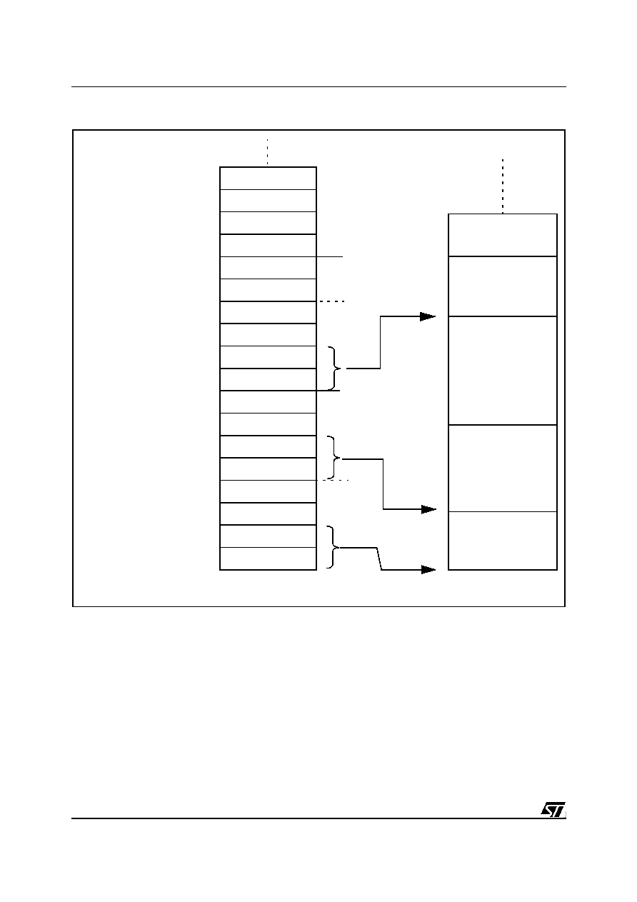
138/230
ST92163 - USB PERIPHERAL (USB)
Figure 73. DMA buffers and related register file locations
8.3.3.3 Interrupt modes
Two interrupt modes are available: single vector,
where the application software has to poll the USB
registers to determine which event required its at-
tention, and multi-vector, where a specific interrupt
vector is used for each endpoint. Special support
is offered to isochronous transfers, implementing a
swapped DMA buffer usage.
8.3.3.4 Suspend mode
The unit can be placed in low-power mode (SUS-
PEND mode), by writing in a control register. At
this time, all static power dissipation is avoided,
except for the generation of the 3.3V supply for the
external pull-up resistor. The detection of activity
at the USB inputs while in low-power mode wakes
the device up asynchronously. A special interrupt
source, ESUSP, is connected directly to a wake-
up line so as to allow the ST9 to exit from HALT
condition.
ADDR0_TH
ADDR0_TL
R0
COUNT0_TH
COUNT0_TL
ADDR0_RH
ADDR0_RL
COUNT0_RH
COUNT0_RL
ADDR1_TH
ADDR1_TL
COUNT1_TH
COUNT1_TL
ADDR1_RH
ADDR1_RL
COUNT1_RH
COUNT1_RL
R1
R2
R3
R4
R5
R6
R7
R8
R9
R10
R11
R12
R13
R14
R15
ADDR2_TH
ADDR2_TL
R16
R17
REGISTER FILE LOCATIONS
TRANSMISSION
BUFFER FOR
ENDPOINT 0
RECEPTION
BUFFER FOR
ENDPOINT 0
TRANSMISSION
BUFFER FOR
ENDPOINT 1
MEMORY AREA
Register File

139/230
ST92163 - USB PERIPHERAL (USB)
USB INTERFACE (Cont'd)
Procedure for entering Suspend Mode
1. Set the TIM_SUSP bit in the USBCTLR register
(bit 6 of R252 in page 15) to suspend the digital
part of the USB cell.
2. Clear both the Wake-up Pending Registers
WUPRH & WUPRL (R254 & R255 in page 57)
to flush all pending wakeup events.
3. Set the LP_SUSP bit in the USBCTLR register
(bit 1 of R252 in page 15) to put the USB cell in
Low Power Suspend mode.
4. Set the ID1S and WKUP-INT bits in the WUC-
TRL register (bit 0 & 1 of R249 in page 57) to
enable the interrupt from the wakeup lines.
5. Write the stop sequence 1, 0, 1 to the STOP bit
of the WUCTRL (bit 2 of R249 in page 57) to
enter stop mode. This stop sequence has to be
executed as continuous sequence of write
instructions without any other register read/
write instructions within the sequence.
6. Insert at least 3 NOP instructions after the stop
sequence in step 5 to allow the MCU clock to
stop.
7. Read the WKCTRL register.
If the STOP bit (bit 2) is 0, it means that the
MCU was stopped and is being woken up by an
external event.
If the STOP bit (bit 2) is 1, it means that the
stop sequence in step 5 was broken by an inter-
rupt or DMA request. In this case, step 5 has to
be executed again until the MCU is stopped.
Procedure for quitting Suspend Mode
There are two ways to wake up the ST9 from Stop
mode: USB bus activity or signal triggering on the
external wakeup lines.
≠ If the MCU is woken up by USB bus activity, an
"End of Suspend" interrupt is generated if it is en-
abled.
≠ If the MCU is woken up by one of the external
wakeup lines, an INTD1 interrupt is generated if
the INTD1 interrupt is enabled and the WKUP-
INT bit in the WUCTRL register (bit 0 of R249 in
page 57) is set.
≠ After the MCU is woken up, wait until the LOCK
bit in the CLK_FLAG register (bit 2 of R242 in
page 55) is at 1 to ensure that the clock PLL is
locked. Then set the CSU_CKSEL bit in the
CLK_FLAG register if it is necessary, since this
bit is cleared by hardware when the MCU stops.
≠ Check the bits in the Wake-up Pending Regis-
ters WU_WUPRH & WU_WUPRL to determine
which pin has woken up the MCU. Then clear the
Wake-up Pending Registers.
Procedure for sending the remote wakeup
(RESUME) signal
After the MCU has been woken up by one of the
external wakeup lines and the source of this wake-
up event is identified, the application may send a
remote wakeup (RESUME) signal using the fol-
lowing procedure:
1. To ensure that the host enables the remote
wakeup feature:
2. Clear the LP_SUSP bit in the USBCTLR regis-
ter (bit 1 of R252 in page 15) to power up the
USB transceiver. Do not clear the TIM_SUSP
bit in the USBCTLR register if an "End of Sus-
pend" interrupt is expected later.
3. Set the RESUME bit in the USBCTLR (bit 3 of
R252 in page 15) to send the RESUME signal.
4. Clear the RESUME bit after 1 to 15 ms, to
ensure that the RESUME signal lasts long
enough.
5. Clear the ESUSP bit in the USBISTR register
(bit 4 of R249 in page 15), since an "End of
Suspend" interrupt is generated by setting
RESUME bit falsely.
6. An "End of Suspend" interrupt will be generated
when the bus activity is resumed by the host, if
the TIM_SUSP bit is not cleared in step 2.
Note: To reduce power consumption during Stop
mode, set as many I/O ports as possible to open
drain output mode and set all ports to 0.

140/230
ST92163 - USB PERIPHERAL (USB)
Example code for Entering Suspend Mode
void Stop_MCU()
{
// Go to the loop to ensure the MCU goes to STOP
do {
spp(0);
EIPR = 0x0;// Clear pending bits
spp(15);
CTLR |= CTR_TIM_SUSP;// Stop USB digital part
spp(57);
WU_WUPRH = 0; // Clear pending bits
WU_WUPRL = 0;
spp(15);
CTLR |= CTR_LP_SUSP;// Stop USB transceiver
spp(57);
WU_CTLR = 0x07;// Set STOP, IDS1 and WKUP-INT bits
WU_CTLR = 0x03;// Set IDS1 and WKUP-INT bit
WU_CTLR = 0x07;// Set STOP, IDS1 and WKUP-INT bits
NOP; NOP; NOP; NOP;
spp(57);
} while (WU_CTLR & 0x04);
}
Example code for sending a RESUME signal
void Remotewakeup()
{
spp(15);
CTLR &= ~CTRLP_SUSP;// Power on the USB transceiver
CTLR |= CTR_RESUME;// Send the RESUME signal
Delay between 1-15ms to keep the RESUME signal
CTLR &= ~CTR_RESUME;// Stop sending RESUME signal
ISTR &= ~INT_ESUSP;// Clear the wrong ESUSP
}

141/230
ST92163 - USB PERIPHERAL (USB)
USB INTERFACE (Cont'd)
8.3.4 Register Description
USB registers can be divided into three groups:
≠ Common registers (page 15): interrupt registers
and USB control registers.
≠ Function and endpoint registers (pages 15, 4
and 5 depending on how many
endpoints are im-
plemented): USB function addresses and end-
point status/configurations.
≠ Extra registers (page 60): device configuration.
8.3.4.1 Common registers
These registers affect all endpoints in the USB in-
terface. They are all mapped in the same ST9 reg-
ister page (page number 15).
The USB interface implements vectorized inter-
rupts: through a vector table it is possible to auto-
matically identify the starting address of each In-
terrupt Service Routine. The vector table contains
the 16-bit addresses pointing to each of the inter-
rupt service routines related to the CTR interrupt
for each endpoint. Other two 8-bit locations are
used to store the address of the service routine
handling the interrupts described in the USBISTR
register. When an interrupt request is acknowl-
edged, the USBIVR register provides a vector
pointing to the location in the vector table, contain-
ing the start address of the interrupt service rou-
tine related to the serviced interrupt.
INTERRUPT VECTOR REGISTER (USBIVR)
R248 - Read/Write
Register page: 15
Reset Value: xxxx xxx0 (xxh)
This register may be used in two different ways de-
pending on the value of the SDNAV bit in the
CTRL register.
≠ If SDNAV bit = 1, Bits 7:1 are user programmable
(bit 0 is fixed to 0). The software writes the ad-
dress of a vector pointing to a single interrupt
routine. The application program has to select
the routine related to the pending interrupts using
the USBISTR and CTRINF registers.
≠ If SDNAV = 0, this register is used as a vector
pointing to the 16-bit interrupt vectors in program
memory containing the start addresses of the in-
terrupt service routines related to the occurred
interrupt. If several interrupts are simultaneously
pending, hardware writes in this register the in-
terrupt routine address related to the highest pri-
ority pending interrupt.
In this case the meaning of each bit is:
Bits 7:6 = A[1:0]:
Vector table Address.
These two bits are user programmable and they
contain the two most significant bits of the interrupt
vector table. This allows the user to define the in-
terrupt vector table position inside the first 256 lo-
cations of program memory at 64 bytes boundary.
Bit 5 = CTRO:
Correct Transfer interrupt occurred
.
0: No CTR interrupt pending
1: One of the interrupt flags in the USBISTR regis-
ter is pending
Note: If several interrupts are simultaneously
pending, hardware writes this bit according to their
relative priorities as listed below starting from the
highest priority one to the lowest priority one:
≠
DMA Over/Underrun (see
Table 26
and USBIS-
TR register description)
≠ Correct Transfer on isochronous endpoints (see
EPnRA register description)
≠ Correct Transfer on non-isochronous endpoints
(see EPnRA register description)
≠
Notification events (see
Table 26
and USBISTR
register description).
Bits 4:1 = V[3:1]:
Endpoint Vector
.
If CTRO = 1, these bits are written by hardware to
specify the endpoint identifier which has generat-
ed the CTR interrupt request.
If several CTR interrupts are pending, hardware
writes the endpoint identifier related to the end-
point with the highest priority. Endpoint priority is
defined according to the following rule: endpoint 0
has the highest priority, then endpoint 1 follows
and so on up to the highest endpoint register pair
(EP15) with the lowest priority.
If CTRO = 0, these bits are fixed to 1. In this case
only one interrupt vector is used for all the inter-
rupts defined in the USBISTR register.
7
0
A1
A0
CTRO
V3
V2
V1
V0
0
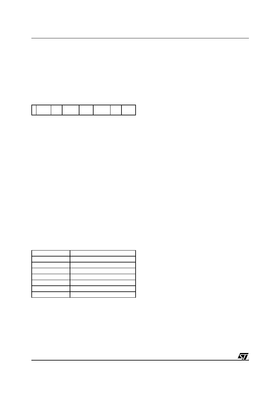
142/230
ST92163 - USB PERIPHERAL (USB)
USB INTERFACE (Cont'd)
Bit 0 = Reserved. This bit is fixed by hardware at 0.
INTERRUPT STATUS REGISTER (USBISTR)
R249 - Read/Write
Register page: 15
Reset Value: 0000 0000 (00h)
Each bit is set by hardware when the related event
occurs.
If one of these bits is set, the hardware clears the
CTRO bit and sets the V[3:0] bits in the USBIVR
register. In this way the USBIVR register will point
to the interrupt vector containing the address of
the service routine related to these interrupt sourc-
es. If several bits are set only a single interrupt will
be generated.
Note: to avoid spurious clearing of some bits, it is
recommended to clear them with a load instruction
where all bits which must not be altered are set to
1, and all bits to be cleared are set to 0. Read-
modify-write instructions like AND, XOR,... are to
be avoided: consider the case of clearing bit 0 of
USBISTR with an AND instruction, when only bit 7
of USBISTR is at 1 and the others at 0. First the
microcontroller reads the content of USBISTR
(=10h), then it clears bit 7 and writes the result
(=00h) in USBISTR. If between the read and the
write operations another bit were set by hardware
(e.g. bit 5), writing 00h would clear it before the mi-
croprocessor has the time to service the event.
Table 26. Classification of Interrupt Sources:
Bit 7 = Reserved. This bit is fixed by hardware at 0.
Bit 6 = DOVR:
DMA over/underrun
.
ST9 processor has not been able to answer a
DMA request in time and the USB FIFO buffer is
full or empty depending on the transfer direction
(reception or transmission).
The USB handles this event in the following way:
during reception the ACK handshake packet is not
sent, during transmission a bit-stuffing error is
forced on the transmitted stream. In both cases
the host will retry the transaction. The DOVR inter-
rupt should never occur during normal operations.
Bit 5 = ERR:
Error
.
One of the errors listed below has occurred:
≠ NANS: No answer. The timeout for a host re-
sponse has expired.
≠ CRC: CRC error. One of the received CRCs, ei-
ther in the token or in the data, was wrong.
≠ BST: Bit Stuffing error. A bit stuffing error was
detected anywhere in the PID, data, and/or CRC.
≠ FVIO: Framing format violation. A nonstandard
frame was received (EOP not in the right place,
wrong token sequence, etc.).
≠ BUFOVR: Buffer overrun. A packet longer than
the allocated DMA buffer has been received.
7
0
0
DOVR
ERR
ESUSP
SUSP
RESET
SOF
ESOF
Interrupt
Class
DOVR
DMA Over/Underrun event
ERR
Notification event
ESUSP
Notification event
SUSP
Notification event
RESET
Notification event
SOF
Notification event
ESOF
Notification event

143/230
ST92163 - USB PERIPHERAL (USB)
USB INTERFACE (Cont'd)
Bit 4 = ESUSP:
End Suspend mode
.
0: No activity detected during Suspend mode
1: USB activity is detected that wakes up the USB
interface during suspend mode.
Note: This event asynchronously clears the
LP_SUSP bit in the USBCTLR register and acti-
vates the WKUP15 internal wake-up line to notify
the WUIMU (if STOP_CK_EN=1 in the
DEVCONF1 register)
Bit 3 = SUSP
Suspend mode request
.
0: No Suspend mode request
1: No USB traffic has been received for 3 ms.
Note: The suspend condition check is enabled im-
mediately after any USB reset and is disabled by
hardware when suspend mode is active
(LP_SUSP = 1) until the end of resume sequence.
Bit 2 = RESET:
USB Reset request
.
0: No USB Reset received.
1: USB Reset received.
Note: Device address and endpoint registers are
reset by an USB reset.
Bit 1 = SOF:
Start Of Frame
.
0: No SOF packet received.
1: SOF packet received.
Bit 0 = ESOF:
Expected Start Of Frame
.
0: No SOF packet missed
1: SOF packet is expected but not received.
INTERRUPT MASK REGISTER (USBIMR)
R250 - Read/Write
Register page: 15
Reset Value: 0000 0000 (00h)
This register contains mask bits for all interrupt
condition bits included in the USBISTR register.
Whenever one of the USBIMR bits is 1, if the cor-
responding USBISTR bit is 1, an interrupt request
is generated. For an explanation of each bit, refer
to the USBISTR register description.
INTERRUPT PRIORITY REGISTER (USBIPR)
R251- Read/Write
Register page: 15
Reset Value: 0xxx 0xxx (xxh)
Bit 7 = IEE:
Isochronous Endpoint Enable
.
Set by software to enable Isochronous Endpoints.
This also enables CTR interrupts related to iso-
chronous endpoints and DMA overrun interrupts.
0: Isochronous endpoints disabled
1: Isochronous endpoints enabled
Bits 6:4 = PIECE[2:0]:
Priority level on Iso-
chronous Endpoint and DMA Over/Underrun
.
Set by software to define the priority level of the is-
ochronous endpoint CTR events (0 is the highest
priority).
Bit 3 = NIEE:
Non-Isochronous Endpoint Enable
.
Set by software to enable Non-Isochronous End-
points. This also enables CTR interrupts related to
non-isochronous (bulk, control, interrupt) end-
points.
0: Non-Isochronous endpoints disabled
1: Non-Isochronous endpoints enabled
Bits 2:0 = PNIEN[2:0]:
Priority level of Non Iso-
chronous Endpoints and Notification.
Set by software to define the priority level of non-
isochronous endpoint (bulk, control, interrupt)
CTR events. 0 is the highest priority.
7
0
0
DOVR
M
ERR
M
ESUSP
M
SUSP
M
RESET
M
SOF
M
ESOF
M
7
0
IEE
PIECE
2
PIECE
1
PIECE
0
NIEE
PNIEN
2
PNIEN
1
PNIEN
0
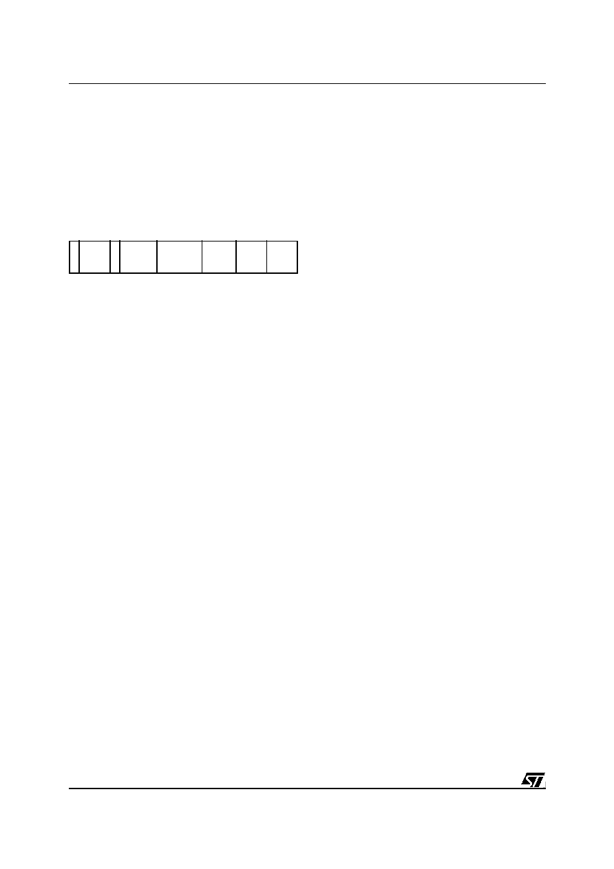
144/230
ST92163 - USB PERIPHERAL (USB)
USB INTERFACE (Cont'd)
Interrupt sources are classified according to the
following table
CONTROL REGISTER (USBCTLR)
R252 - Read/Write
Register page: 15
Reset Value: 0001 0101 (15h)
Bit 7 = Reserved. This bit is fixed by hardware at 0.
Bit 6 = TIM_SUSP:
Timed Suspend
.
Set by software when the SUSP interrupt is re-
ceived to enter "timed-suspend" state.
0: Timed suspend inactive
1: Timed suspend active. The USB interface oper-
ates as in suspend mode but clocks and static
power dissipation in the analog transceiver are
not stopped.
Bit 5 = Reserved.
Bit 4 = SDNAV:
Single/Multiple Vector Selection
.
This bit is set by software to select the single or
multiple interrupt vector mode .
0: Multiple interrupt vector mode
1: Single interrupt vector mode
See USBIVR register description for detailed infor-
mation.
Bit 3 = RESUME:
Resume request
.
Set by software to send a Resume signal to the
host.
0: Resume signal not forced on USB data lines.
1: Resume signal forced on USB data lines.
Bit 2 = PDWN:
Power Down
.
Set by software to turn off the 3.3V on-chip voltage
regulator that supplies the external pull-up resistor
and the transceiver.
Note: As a consequence the voltage on both USB
root port signal lines will drift to 0V because of the
pull-down resistors in the upstream USB host or
hub, generating a disconnect indication. At least 2
µ
s are required until the 3.3V supply falls within
specifications after this bit is cleared, depending
on the value of the external bypass capacitor.
Bit 1 = LP_SUSP:
Low-power suspend
.
Set by software to put the USB interface in "low-
power suspend" state. This condition should be
entered while in "timed suspend" state
(TIM_SUSP=1).
0: Low-power suspend inactive
1: Low-power suspend active
Bit 0 = FRES:
Force USB Reset
.
Set by software to force a reset of the USB inter-
face, just like a RESET signal on the USB. The
USB interface is held in RESET state until soft-
ware clears this bit, and a "USB-RESET" interrupt
is generated, if enabled.
0: Reset not forced
1: USB interface reset forced
7
0
0
TIM_
SUSP
0
SDNAV
RESUME
PDWN
LP_
SUSP
FRES

145/230
ST92163 - USB PERIPHERAL (USB)
USB INTERFACE (Cont'd)
CTR INTERRUPT FLAGS (CTRINF)
R253 - Read/Write
Register page: 15
Reset Value: 00xx xxx0 (xxh)
Note: This register is used only when the SDNAV
bit is 1.
Bit 7:6 = Reserved. These bits are fixed by hard-
ware at 0.
Bit 5 = INTO:
Interrupt occurred
.
Set by hardware when SDNAV = 1 in the same
way as the CTRO bit in USBIVR register is set
when SDNAV = 0.
Bit 4:1 = ENID[3:0]:
Endpoint identifier
.
Set by hardware when SDNAV = 1 in the same
way as V[3:0] bits in USBIVR register are set when
SDNAV = 0.
Bit 0 = Reserved. This bit is fixed by hardware at 0.
FRAME NUMBER REGISTER HIGH (FNRH)
R254 - Read-only
Register page: 15
Reset Value: 0000 0xxx (0xh)
Bit 7 = RXDP.
Set/cleared by hardware to indicate D+ upstream
port data line status.
Bit 6 = RXDM.
Set/cleared by hardware to indicate D- upstream
port data line status.
Bit 5 = LCK:
Locked
.
Set by hardware when at least two consecutive
SOF packets have been received after the end of
a USB reset condition or after the end of a USB
resume sequence.
0: Frame timer not locked
1: Frame timer locked
Note: Once locked, the frame timer remains in this
state until a USB reset or USB suspend event oc-
curs.
Bits 4:3 = LSOF[1:0]:
Lost SOF
.
Set by hardware when an ESOF interrupt is gener-
ated, counting the number of consecutive SOF
packets lost. On reception of a SOF packet, these
bits are cleared.
Bits 2:0 = FN[10:8]:
Frame Number bits 10:8
.
These bits contain the most significant bits of the
Frame number received with the last received
SOF packet. These bits are updated when a SOF
interrupt is generated.
FRAME NUMBER REGISTER LOW (FNRL)
R255 - Read-only
Register page: 15
Reset Value: xxxx xxxx (xxh)
Bits 7:0 = FN[7:0]:
Frame Number bits 7:0
.
Set by hardware, this register contains the least
significant bits of the 11-bit frame number con-
tained in the last received SOF packet. The 3 re-
maining most significant bits are stored in the
FNRH register. This register is updated when a
SOF interrupt is generated.
8.3.4.2 Device and Endpoint specific Registers
For each function a DADDR register is available to
store the device address and for each endpoint a
pair of EPnR registers is available to store end-
point specific information.
7
0
0
0
INTO
ENID3 ENID2 ENID1 ENID0
0
7
0
RXDP RXDM
LCK
LSOF1 LSOF0 FN10
FN9
FN8
7
0
FN7
FN6
FN5
FN4
FN3
FN2
FN1
FN0

146/230
ST92163 - USB PERIPHERAL (USB)
USB INTERFACE (Cont'd)
DEVICE n ADDRESS (DADDRn)
R240 to R247 - Read/Write
Register page: 15
Reset Value: 0000 0000 (00h)
Note: This register is also reset when a USB reset
is received from the USB bus or forced through bit
FRES in the USBCTLR register.
Bit 7 = EF:
Enable Function
.
Set by software to enable the USB function whose
address is contained in the following ADD[6:0]
bits.
0: Function disabled
1: Function enabled
Bits 6:0 = ADD[6:0]:
Device Address
.
Software must write into these bits the USB device
address assigned by the host PC during the enu-
meration.
ENDPOINT n REGISTER A (EPnRA)
(TRANSMISSION)
R240-R254 (even)
Read/Write
Register pages: 4 & 5
Reset value: 0000 0000 (00h)
These registers are used for controlling data trans-
mission. They are also reset when a USB reset is
received or forced through the FRES bit in the US-
BCTLR register.
Note: The CTR bits are not affected by a USB re-
set
Each endpoint has its EPnRA register where n is
the endpoint identifier in the range 0 to 15.
Bit 7 = CTR:
Correct Transfer
.
Set by hardware when a transaction is successful-
ly completed on this endpoint; software can only
clear this bit.
0: No correct transfer occurred
1: Correct transfer occurred
Note: A transaction ended with a NAK or STALL
handshake does not set this bit, since no data is
actually transferred, as in the case of protocol er-
rors or data toggle mismatches. The CTR bit is
also used to perform flow control: while CTR=1, a
valid endpoint answers NAK to every transaction
addressed to it (except SETUP requests which are
simply ignored) until the application software ac-
knowledges the CTR event, resetting this bit. This
does not apply to isochronous endpoints where no
handshake phase is used.
Bit 6 = DTOG_TX:
Data Toggle, for transmission
transfers
.
If the endpoint is non-isochronous, this bit contains
the required value of the data toggle bit
(0=DATA0, 1=DATA1) for the next data packet to
be transmitted. Hardware toggles this bit when the
ACK handshake is received from the USB host,
following a data packet transmission. If the end-
point is defined as a control one, hardware sets
this bit to 1 on reception of a SETUP PID ad-
dressed to this endpoint.
If the endpoint is isochronous, this bit is used to
support DMA buffer swapping since no data tog-
gling is used for this sort of endpoint and only
DATA0 packet are transmitted. Hardware toggles
this bit just after the end of data packet transmis-
sion, since no handshake is used for isochronous
transfers.
Note: this bit can be also written by software to in-
itialize it (mandatory when the endpoint is not a
control endpoint) or to force specific data toggle/
DMA buffer usage.
7
0
EF
ADD6
ADD5
ADD4
ADD3
ADD2
ADD1
ADD0
7
0
CTR
DTOG_
TX
STAT_
TX1
STAT_
TX0
PIDR1 PIDR0
CEP
ISO

147/230
ST92163 - USB PERIPHERAL (USB)
USB INTERFACE (Cont'd)
Bit 5:4 = STAT_TX [1:0]
Status bits, for transmis-
sion transfers
.
These bits contain the information about the end-
point status, which are listed below:
Table 27. Transmission status encoding
These bits are written by software, but hardware
sets the STAT_TX bits to NAK when a correct
transfer has occurred (CTR=1) related to a IN or
SETUP (control only) transaction addressed to
this endpoint, waiting for the software to prepare
the next set of data to be transmitted. If the end-
point is defined as isochronous, its status can be
only "VALID" or "DISABLED" so no hardware
change of the endpoint status will take place after
a successful transaction.
Bits 3:2 = PIDR[1:0]:
PID Received
.
These bits are read-only and contain the two most
significant bits of the PID field of the last token PID
addressed to this endpoint.
These bits are kept frozen while CTR bit is at 1.
The USB standard defines PIDR bits as in the fol-
lowing table:
Table 28. PID encoding
Bit 1 = CEP:
Control Endpoint
.
Software must set this bit to configure this end-
point as a control endpoint.
0: Non-control endpoint
1: Control endpoint
Notes: If a control endpoint is defined as NAK in
the receive direction, the USB interface will not an-
swer, when a SETUP transaction is received.
If the control endpoint is defined as STALL in the
receive direction, then the SETUP packet will be
accepted anyway, transferring data and issuing
the CTR interrupt.
Bit 0 = ISO:
Isochronous endpoint
.
Software must set this bit to configure this end-
point as an isochronous endpoint.
0: Not an isochronous endpoint
1:isochronous endpoint
Note: Since isochronous transfer has no hand-
shake phase, the only legal values for the
STAT_RX/STAT_TX bit pairs are `00' (Disabled)
and `11' (Valid), any other value will produce re-
sults not compliant to the USB standard. Iso-
chronous endpoints implement double-buffering,
using both `transmission' and `reception' memory
areas to manage buffer swapping on each suc-
cessful transaction.
The memory buffer that is currently used by the
USB interface is defined by the DTOG bit corre-
sponding to the endpoint direction (DTOG_RX in
EPnRB for `reception' isochronous endpoints,
DTOG_TX in EPnRA for `transmission' iso-
chronous endpoints) according to the following ta-
ble:
Table 29. Isochronous memory buffers usage
Since the swapped buffer management requires
the usage of all 8 Register File locations hosting
the address pointer and the length of the allocated
memory buffers, isochronous endpoints are forced
to be unidirectional so it is not possible to enable
an isochronous endpoint both for transmission and
reception.
STAT_TX
[1:0]
Meaning
00
DISABLED: all transmission requests ad-
dressed to this endpoint are ignored.
01
STALL: the endpoint is stalled and all trans-
mission requests result in a STALL hand-
shake.
10
NAK: the endpoint is NAKed and all trans-
mission requests result in a NAK hand-
shake.
11
VALID: this endpoint is enabled for trans-
mission.
PIDR[1:0]
PID
00
OUT
10
IN
11
SETUP
DTOG bit
value
DMA buffer used by
USB Interface
DMA buffer used by
application
software
0
ADDRn_T /
COUNTn_T register
file locations.
ADDRn_R /
COUNTn_R register
file locations.
1
ADDRn_R /
COUNTn_R register
file locations.
ADDRn_T /
COUNTn_T register
file locations.
148/230
ST92163 - USB PERIPHERAL (USB)
USB INTERFACE (Cont'd)
ENDPOINT n REGISTER B (EPnRB)
(RECEPTION)
R241-R255 (odd) - Read/Write
Register pages: 4 & 5
Reset value: 0000 0000 (00h)
These registers are used for controlling data re-
ception. They are also reset when a USB reset is
received from the USB bus or forced through bit
FRES in the USBCTLR register. Each endpoint
has its EPnRB register where n is the endpoint
identifier in the range 0 to 15.
Bit 7 = ST_OUT
Status out
.
This bit is set by software to indicate that a status
out transaction is expected: in this case all OUT
transactions containing more than zero data bytes
are answered STALL instead of ACK. This bit may
be used to improve the robustness of the applica-
tion to protocol errors during control transfers and
its usage is intended on control endpoints only.
When ST_OUT is reset, OUT transactions can
have any number of bytes, as needed.
Bit 6 = DTOG_RX:
Data Toggle, for reception
transfers
.
If the endpoint is non-isochronous, this bit contains
the expected value of the data toggle bit
(0=DATA0, 1=DATA1) for the next data packet to
be received. Hardware toggles this bit when the
ACK handshake is sent to the USB host, following
a data packet reception with a matching data PID
value. If the endpoint is defined as a control end-
point, hardware resets this bit on reception of a
SETUP PID addressed to this endpoint.
If the endpoint is isochronous, this bit is used to
support DMA buffer swapping since no data tog-
gling is used for this sort of endpoint and only
DATA0 packets are received. Hardware toggles
this bit just after the end of data packet reception,
since no handshake is used for isochronous trans-
fers.
Note: this bit can be also written by software to in-
itialize it (mandatory when the endpoint is not a
control endpoint) or to force a specific data toggle/
DMA buffer usage.
Bit 5:4 = STAT_RX [1:0]
Status bits, for reception
transfers
.
These bits contain the information about the end-
point status, as listed below:
Table 30. Reception status encoding
These bits are written by software, but hardware
sets the STAT_RX bits to NAK when a correct
transfer has occurred (CTR=1) related to a OUT or
SETUP (control only) transaction addressed to
this endpoint, so software has time to interpret the
received data before acknowledging a new trans-
action.
If the endpoint is defined as isochronous, its status
can be only "VALID" or "DISABLED" so no hard-
ware change of the endpoint status will take place
after a successful transaction.
Bit 3:0 = EnA[3:0]
Endpoint n Address, bits 3-0.
Software must write in this field the 4-bit address
used to identify the transactions directed to this
endpoint. A value must be written before enabling
the corresponding endpoint.
7
0
ST_OU
T
DTOG_
RX
STAT_
RX1
STAT_
RX0
EnA3
EnA2
EnA1
EnA0
STAT_TX
[1:0]
Meaning
00
DISABLED: all reception requests ad-
dressed to this endpoint are ignored.
01
STALL: the endpoint is stalled and all re-
ception requests result in a STALL hand-
shake.
10
NAK: the endpoint is naked and all recep-
tion requests result in a NAK handshake.
11
VALID: this endpoint is enabled for recep-
tion.
149/230
ST92163 - USB PERIPHERAL (USB)
USB INTERFACE (Cont'd)
8.3.4.3 Miscellaneous Registers
These registers contain device configuration pa-
rameters or optional functions of USB interface.
DEVICE CONFIGURATION 1 (DEVCONF1)
R244 - Read/Write
Register page: 60
Reset value: 0000 1111 (0Fh)
This register contains device configuration data
that should be written by the software at the begin-
ning of the application program and should never
be changed during normal operations.
Bit 7:6 = Reserved. This bit is fixed by hardware at
0.
Bit 6 = Reserved. Must be kept at 0.
Bit 5 = USBOE_EN:
USBOE Signal Enable
.
Set by software to enable the alternate output
function connected to the upstream output enable
signal.
1: USBOE signal output enabled
0: USBOE signal output disabled
Bit 4 = Reserved.
Bits 3:0 = Reserved. These bits are fixed by hard-
ware at 1.
DEVICE CONFIGURATION 2 (DEVCONF2)
R245 - Read/Write
Register page: 60
Reset value: 0000 0000 (00h)
This register contains device configuration data
that should be written by the software at the begin-
ning of the application program and should never
be changed during normal operations.
Bits 7:2 = Reserved. These bits must be always
written to 0.
Bit 1 = LVD_DISABLE:
Low Voltage Detector Dis-
able
Set by the software to disable the generation of
the device reset signal by the LVD.
1: LVD disabled
0: LVD enabled
If this bit is at 0, an internal reset can be issued
both by the external RESET pin and the LVD when
it detects a low supply voltage; if this bit is at 1 only
the external pad can start a device reset.
Note: this bit can be only set to 1 by software, writ-
ing 0 has no effect and the LVD can be re-enabled
only using a device reset.
7
0
0
-
USBOE
_EN
LS_
DEVICE
1
1
1
1
7
0
0
0
0
0
0
0
LVD_
DISABLE
SOFP_
ENABLE

150/230
ST92163 - USB PERIPHERAL (USB)
USB INTERFACE (Cont'd)
Bit 0 = SOFP_ENABLE:
Start-Of-Frame Pulse
Enable.
Set by software to enable the use of the USBSOF
alternate output function.
1: USBSOF alternate function enabled
0: USBSOF output disabled
USBSOF outputs a 333.33 ns long pulse at each
frame start (actually 10 bits before the SOF packet
expected start). This pulse is not generated until
two SOF packets are received after any USB reset
or USB resume (frame timer locking) and they stop
as soon as the suspend condition is entered
(TIM_SUSP bit in USBCTLR register).
MIRROR REGISTER A (MIRRA)
R246 - Read/Write
Register page: 60
Reset value: xxxx xxxx (xxh)
Bit 7:0 = MIRA[7:0]
Mirror register A, bits 7-0.
This register acts as a bit mirroring location where
software can write a byte and read it back with the
LSB and MSB position swapped.
MIRROR REGISTER B (MIRRB)
R247 - Read/Write
Register page: 60
Reset value: xxxx xxxx (xxh)
Bit 7:0 = MIRB[7:0]
Mirror register B, bits 7-0.
This register acts as a bit mirroring location where
software can write a byte and read it back with the
LSB and MSB position swapped.
7
0
MIRA7 MIRA6 MIRA5 MIRA4 MIRA3 MIRA2 MIRA1 MIRA0
7
0
MIRB7 MIRB6 MIRB5 MIRB4 MIRB3 MIRB2 MIRB1 MIRB0
151/230
ST92163 - USB PERIPHERAL (USB)
USB INTERFACE (Cont'd)
8.3.5 Register pages summary
The registers are located in different register file
pages. To help finding the correct page for each
register, the following tables show the page map-
ping of all USB registers.
Table 31. USB Register Page Mapping
Table 32. USB Register page 15 Map and Reset Values
Address
Page 4
Page 5
Page 15
Page 60
240 (F0h)
EP0RA
EP8RA
DADDR0
241 (F1h)
EP0RB
EP8RB
DADDR1
242 (F2h)
EP1RA
EP9RA
DADDR2
243 (F3h)
EP1RB
EP9RB
DADDR3
244 (F4h)
EP2RA
EP10RA
DADDR4
DEVCONF1
245 (F5h)
EP2RB
EP10RB
DADDR5
DEVCONF2
246 (F6h)
EP3RA
EP11RA
DADDR6
MIRRA
247 (F7h)
EP3RB
EP11RB
DADDR7
MIRRB
248 (F8h)
EP4RA
EP12RA
USBIVR
249 (F9h)
EP4RB
EP12RB
USBISTR
250 (FAh)
EP5RA
EP13RA
USBIMR
251 (FBh)
EP5RB
EP13RB
USBIPR
252 (FCh)
EP6RA
EP14RA
USBCTLR
253 (FDh)
EP6RB
EP14RB
CTRINF
254 (FEh)
EP7RA
EP15RA
FNRH
255 (FFh)
EP7RB
EP15RB
FNRL
Reg.
No.
Register
Name
7
6
5
4
3
2
1
0
R240
-
R247
DADDRn
Reset Value
EF
0
ADD6
0
ADD5
0
ADD4
0
ADD3
0
ADD2
0
ADD1
0
ADD0
0
R248
USBIVR
Reset Value
A1
x
A0
x
CTRO
x
V3
x
V2
x
V1
x
V0
x
0
0
R249
USBISTR
Reset Value
0
0
DOVR
0
DOVR
0
ESUSP
0
SUSP
0
RESET
0
SOF
0
ESOF
0
R250
USBIMR
Reset Value
0
0
DOVRM
0
DOVRM
0
ESUSPM
0
SUSPM
0
RESETM
0
SOFM
0
ESOFM
0
R251
USBIPR
Reset Value
IEE
0
PIECE2
x
PIECE1
x
PIECE0
x
NIEE
0
PNIEN2
x
PNIEN1
x
PNIEN0
x
R252
USBCTLR
Reset Value
0
0
TIM_SUSP
0
0
0
SDNAV
1
RESUME
0
PDWN
1
LP_SUSP
0
FRES
1

152/230
ST92163 - USB PERIPHERAL (USB)
R253
CTRINF
Reset Value
0
0
0
0
INTO
x
ENID3
x
ENID2
x
ENID1
x
ENID0
x
0
0
R254
FNRH
Reset Value
RXDP
0
RXDM
0
LCK
0
LSOF1
0
LSOF0
0
FN10
x
FN9
x
FN8
x
R255
FNRL
Reset Value
FN7
x
FN6
x
FN5
x
FN4
x
FN3
x
FN2
x
FN1
x
FN0
x
Reg.
No.
Register
Name
7
6
5
4
3
2
1
0
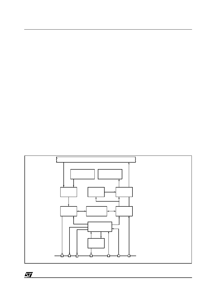
153/230
ST92163 - MULTIPROTOCOL SERIAL COMMUNICATIONS INTERFACE (SCI-M)
8.4 MULTIPROTOCOL SERIAL COMMUNICATIONS INTERFACE (SCI-M)
8.4.1 Introduction
The Multiprotocol Serial Communications Inter-
face (SCI-M) offers full-duplex serial data ex-
change with a wide range of external equipment.
The SCI-M offers four operating modes: Asynchro-
nous, Asynchronous with synchronous clock, Seri-
al expansion and Synchronous.
8.4.2 Main Features
s
Full duplex synchronous and asynchronous
operation.
s
Transmit, receive, line status, and device
address interrupt generation.
s
Integral Baud Rate Generator capable of
dividing the input clock by any value from 2 to
2
16
-1 (16 bit word) and generating the internal
16X data sampling clock for asynchronous
operation or the 1X clock for synchronous
operation.
s
Fully programmable serial interface:
≠ 5, 6, 7, or 8 bit word length.
≠ Even, odd, or no parity generation and detec-
tion.
≠ 0, 1, 1.5, 2, 2.5, 3 stop bit generation.
≠ Complete status reporting capabilities.
≠ Line break generation and detection.
s
Programmable address indication bit (wake-up
bit) and user invisible compare logic to support
multiple microcomputer networking. Optional
character search function.
s
Internal diagnostic capabilities:
≠ Local loopback for communications link fault
isolation.
≠ Auto-echo for communications link fault isola-
tion.
s
Separate interrupt/DMA channels for transmit
and receive.
s
In addition, a Synchronous mode supports:
≠ High speed communication
≠ Possibility of hardware synchronization (RTS/
DCD signals).
≠ Programmable polarity and stand-by level for
data SIN/SOUT.
≠ Programmable active edge and stand-by level
for clocks CLKOUT/RXCL.
≠ Programmable active levels of RTS/DCD sig-
nals.
≠ Full Loop-Back and Auto-Echo modes for DA-
TA, CLOCKs and CONTROLs.
Figure 74. SCI-M Block Diagram
TRANSMIT
BUFFER
REGISTER
REGISTER
SHIFT
TRANSMIT
REGISTER
SHIFT
RECEIVER
FUNCTION
ALTERNATE
REGISTER
COMPARE
ADDRESS
REGISTER
BUFFER
RECEIVER
DMA
CONTROLLER
CLOCK and
BAUD RATE
GENERATOR
ST9 CORE BUS
SOUT
TXCLK/CLKOUT RXCLK
SIN
VA00169A
Frame Control
and STATUS
DMA
CONTROLLER
RTS
DCD
SDS

154/230
ST92163 - MULTIPROTOCOL SERIAL COMMUNICATIONS INTERFACE (SCI-M)
MULTIPROTOCOL SERIAL COMMUNICATIONS INTERFACE (Cont'd)
8.4.3 Functional Description
The SCI-M has four operating modes:
≠ Asynchronous mode
≠ Asynchronous mode with synchronous clock
≠ Serial expansion mode
≠ Synchronous mode
Asynchronous mode, Asynchronous mode with
synchronous clock and Serial expansion mode
output data with the same serial frame format. The
differences lie in the data sampling clock rates
(1X, 16X) and in the protocol used.
Figure 75. SCI -M Functional Schematic
Note: Some pins may not be available on some devices. Refer to the device Pinout Description.
Divider by 16
1
0
1
0
Divider by 16
CD
CD
The control signals marked with (*) are active only in synchronous mode (SMEN=1)
Polarity
Polarity
TXclk / CLKout
RX shift
register
TX buffer
register
TX shift
register
RTSEN (*)
Enveloper
AEN (*)
OUTSB (*)
s
t
an
d by
pol
ar
i
t
y
Sout
AEN
RX buffer
register
p
olarity
pola
rity
s
t
an
d by
pol
a
r
i
t
y
Baud rate
generator
RXclk
OCKSB (*)
LBEN (*)
INTCLK
XBRG
AEN (*)
OCLK
XTCLK
DCDEN (*)
DCD
RTS
Sin
INPL (*)
LBEN
OUTPL (*)
INPEN (*)
OCKPL (*)
XRX
OCLK
VR02054
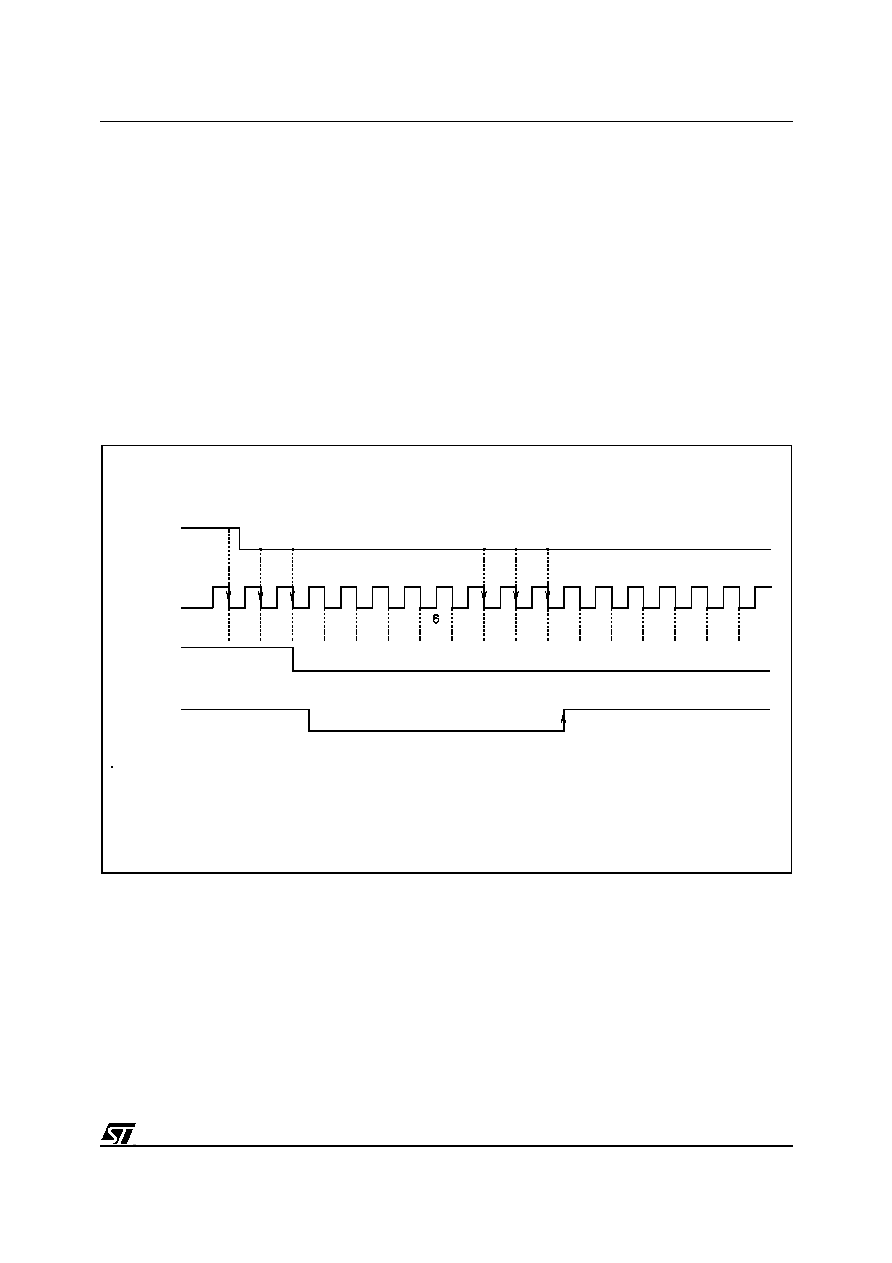
155/230
ST92163 - MULTIPROTOCOL SERIAL COMMUNICATIONS INTERFACE (SCI-M)
MULTIPROTOCOL SERIAL COMMUNICATIONS INTERFACE (Cont'd)
8.4.4 SCI-M Operating Modes
8.4.4.1 Asynchronous Mode
In this mode, data and clock can be asynchronous
(the transmitter and receiver can use their own
clocks to sample received data), each data bit is
sampled 16 times per clock period.
The baud rate clock should be set to the ˜16 Mode
and the frequency of the input clock (from an ex-
ternal source or from the internal baud-rate gener-
ator output) is set to suit.
8.4.4.2 Asynchronous Mode with Synchronous
Clock
In this mode, data and clock are synchronous,
each data bit is sampled once per clock period.
For transmit operation, a general purpose I/O port
pin can be programmed to output the CLKOUT
signal from the baud rate generator. If the SCI is
provided with an external transmission clock
source, there will be a skew equivalent to two
INTCLK periods between clock and data.
Data will be transmitted on the falling edge of the
transmit clock. Received data will be latched into
the SCI on the rising edge of the receive clock.
Figure 76. Sampling Times in Asynchronous Format
0
1
2
3
4
5
7
8
9
10
11
12
13
14
15
SDIN
rcvck
rxd
rxclk
VR001409
LEGEND:
SIN:
rcvck:
rxd:
rxclk:
Serial Data Input line
Internal X16 Receiver Clock
Internal Serial Data Input Line
Internal Receiver Shift Register Sampling Clock

156/230
ST92163 - MULTIPROTOCOL SERIAL COMMUNICATIONS INTERFACE (SCI-M)
MULTIPROTOCOL SERIAL COMMUNICATIONS INTERFACE (Cont'd)
8.4.4.3 Serial Expansion Mode
This mode is used to communicate with an exter-
nal synchronous peripheral.
The transmitter only provides the clock waveform
during the period that data is being transmitted on
the CLKOUT pin (the Data Envelope). Data is
latched on the rising edge of this clock.
Whenever the SCI is to receive data in serial port
expansion mode, the clock must be supplied ex-
ternally, and be synchronous with the transmitted
data. The SCI latches the incoming data on the ris-
ing edge of the received clock, which is input on
the RXCLK pin.
8.4.4.4 Synchronous Mode
This mode is used to access an external synchro-
nous peripheral, dummy start/stop bits are not in-
cluded in the data frame. Polarity, stand-by level
and active edges of I/O signals are fully and sepa-
rately programmable for both inputs and outputs.
It's necessary to set the SMEN bit of the Synchro-
nous Input Control Register (SICR) to enable this
mode and all the related extra features (otherwise
disabled).
The transmitter will provide the clock waveform
only during the period when the data is being
transmitted via the CLKOUT pin, which can be en-
abled by setting both the XTCLK and OCLK bits of
the Clock Configuration Register. Whenever the
SCI is to receive data in synchronous mode, the
clock waveform must be supplied externally via
the RXCLK pin and be synchronous with the data.
For correct receiver operation, the XRX bit of the
Clock Configuration Register must be set.
Two external signals, Request-To-Send and Data-
Carrier-Detect (RTS/DCD), can be enabled to syn-
chronise the data exchange between two serial
units. The RTS output becomes active just before
the first active edge of CLKOUT and indicates to
the target device that the MCU is about to send a
synchronous frame; it returns to its stand-by state
following the last active edge of CLKOUT (MSB
transmitted).
The DCD input can be considered as a gate that
filters RXCLK and informs the MCU that a trans-
mitting device is transmitting a data frame. Polarity
of RTS/DCD is individually programmable, as for
clocks and data.
The data word is programmable from 5 to 8 bits, as
for the other modes; parity, address/9th, stop bits
and break cannot be inserted into the transmitted
frame. Programming of the related bits of the SCI
control registers is irrelevant in Synchronous
Mode: all the corresponding interrupt requests
must, in any case, be masked in order to avoid in-
correct operation during data reception.
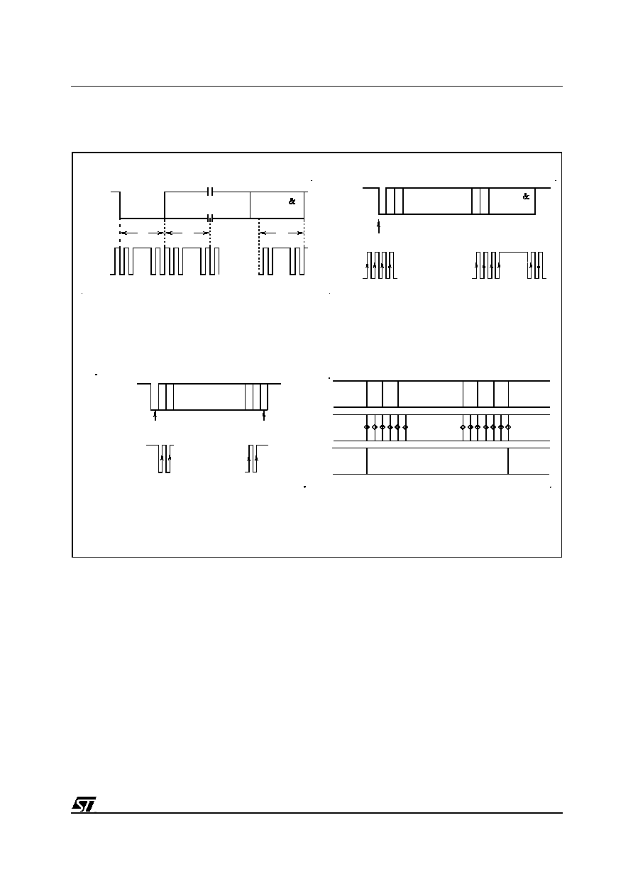
157/230
ST92163 - MULTIPROTOCOL SERIAL COMMUNICATIONS INTERFACE (SCI-M)
MULTIPROTOCOL SERIAL COMMUNICATIONS INTERFACE (Cont'd)
Figure 77. SCI -M Operating Modes
Note: In all operating modes, the Least Significant Bit is transmitted/received first.
Asynchronous Mode
Asynchronous Mode
with Synchronous Clock
Serial Expansion Mode
Synchronous Mode
I/O
CLOCK
START BIT
DATA
PARITY
STOP BIT
16
16
16
VA00271
I/O
CLOCK
START BIT
DATA
PARITY
STOP BIT
VA00272
I/O
CLOCK
DATA
VA0273A
START BIT
(Dummy)
STOP BIT
(Dummy)
stand-by
CLOCK
DATA
VR02051
stand-by
stand-by
stand-by
RTS/DCD
stand-by
stand-by
158/230
ST92163 - MULTIPROTOCOL SERIAL COMMUNICATIONS INTERFACE (SCI-M)
MULTIPROTOCOL SERIAL COMMUNICATIONS INTERFACE (Cont'd)
8.4.5 Serial Frame Format
Characters sent or received by the SCI can have
some or all of the features in the following format,
depending on the operating mode:
START: the START bit indicates the beginning of
a data frame in Asynchronous modes. The START
condition is detected as a high to low transition.
A dummy START bit is generated in Serial Expan-
sion mode. The START bit is not generated in
Synchronous mode.
DATA: the DATA word length is programmable
from 5 to 8 bits, for both Synchronous and Asyn-
chronous modes. LSB are transmitted first.
PARITY: The Parity Bit (not available in Serial Ex-
pansion mode and Synchronous mode) is option-
al, and can be used with any word length. It is used
for error checking and is set so as to make the total
number of high bits in DATA plus PARITY odd or
even, depending on the number of "1"s in the
DATA field.
ADDRESS/9TH: The Address/9th Bit is optional
and may be added to any word format. It is used in
both Serial Expansion and Asynchronous modes
to indicate that the data is an address (bit set).
The ADDRESS/9TH bit is useful when several mi-
crocontrollers are exchanging data on the same
serial bus. Individual microcontrollers can stay idle
on the serial bus, waiting for a transmitted ad-
dress. When a microcontroller recognizes its own
address, it can begin Data Reception, likewise, on
the transmit side, the microcontroller can transmit
another address to begin communication with a
different microcontroller.
The ADDRESS/9TH bit can be used as an addi-
tional data bit or to mark control words (9th bit).
STOP: Indicates the end of a data frame in Asyn-
chronous modes. A dummy STOP bit is generated
in Serial Expansion mode. The STOP bit can be
programmed to be 1, 1.5, 2, 2.5 or 3 bits long, de-
pending on the mode. It returns the SCI to the qui-
escent marking state (i.e., a constant high-state
condition) which lasts until a new start bit indicates
an incoming word. The STOP bit is not generated
in Synchronous mode.
Figure 78. SCI Character Formats
(1)
LSB First
(2)
Not available in Synchronous mode
(3)
Not available in Serial Expansion mode
and Synchronous mode
START
(2)
DATA
(1)
PARITY
(3)
ADDRESS
(2)
STOP
(2)
# bits
1
5, 6, 7, 8
0, 1
0, 1
1, 1.5, 2, 2.5,
1, 2, 3
16X
1X
states
NONE
ODD
EVEN
ON
OFF

159/230
ST92163 - MULTIPROTOCOL SERIAL COMMUNICATIONS INTERFACE (SCI-M)
MULTIPROTOCOL SERIAL COMMUNICATIONS INTERFACE (Cont'd)
8.4.5.1 Data transfer
Data to be transmitted by the SCI is first loaded by
the program into the Transmitter Buffer Register.
The SCI will transfer the data into the Transmitter
Shift Register when the Shift Register becomes
available (empty). The Transmitter Shift Register
converts the parallel data into serial format for
transmission via the SCI Alternate Function out-
put, Serial Data Out. On completion of the transfer,
the transmitter buffer register interrupt pending bit
will be updated. If the selected word length is less
than 8 bits, the unused most significant bits do not
need to be defined.
Incoming serial data from the Serial Data Input pin
is converted into parallel format by the Receiver
Shift Register. At the end of the input data frame,
the valid data portion of the received word is trans-
ferred from the Receiver Shift Register into the Re-
ceiver Buffer Register. All Receiver interrupt con-
ditions are updated at the time of transfer. If the
selected character format is less than 8 bits, the
unused most significant bits will be set.
The Frame Control and Status block creates and
checks the character configuration (Data length
and number of Stop bits), as well as the source of
the transmitter/receiver clock.
The internal Baud Rate Generator contains a pro-
grammable divide by "N" counter which can be
used to generate the clocks for the transmitter
and/or receiver. The baud rate generator can use
INTCLK or the Receiver clock input via RXCLK.
The Address bit/D9 is optional and may be added
to any word in Asynchronous and Serial Expan-
sion modes. It is commonly used in network or ma-
chine control applications. When enabled (AB set),
an address or ninth data bit can be added to a
transmitted word by setting the Set Address bit
(SA). This is then appended to the next word en-
tered into the (empty) Transmitter Buffer Register
and then cleared by hardware. On character input,
a set Address Bit can indicate that the data pre-
ceding the bit is an address which may be com-
pared in hardware with the value in the Address
Compare Register (ACR) to generate an Address
Match interrupt when equal.
The Address bit and Address Comparison Regis-
ter can also be combined to generate four different
types of Address Interrupt to suit different proto-
cols, based on the status of the Address Mode En-
able bit (AMEN) and the Address Mode bit (AM) in
the CHCR register.
The character match Address Interrupt mode may
be used as a powerful character search mode,
generating an interrupt on reception of a predeter-
mined character e.g. Carriage Return or End of
Block codes (Character Match Interrupt). This is
the only Address Interrupt Mode available in Syn-
chronous mode.
The Line Break condition is fully supported for both
transmission and reception. Line Break is sent by
setting the SB bit (IDPR). This causes the trans-
mitter output to be held low (after all buffered data
has been transmitted) for a minimum of one com-
plete word length and until the SB bit is Reset.
Break cannot be inserted into the transmitted
frame for the Synchronous mode.
Testing of the communications channel may be
performed using the built-in facilities of the SCI pe-
ripheral. Auto-Echo mode and Loop-Back mode
may be used individually or together. In Asynchro-
nous, Asynchronous with Synchronous Clock and
Serial Expansion modes they are available only on
SIN/SOUT pins through the programming of AEN/
LBEN bits in CCR. In Synchronous mode (SMEN
set) the above configurations are available on SIN/
SOUT, RXCLK/CLKOUT and DCD/RTS pins by
programming the AEN/LBEN bits and independ-
ently of the programmed polarity. In the Synchro-
nous mode case, when AEN is set, the transmitter
outputs (data, clock and control) are disconnected
from the I/O pins, which are driven directly by the
receiver input pins (Auto-Echo mode: SOUT=SIN,
CLKOUT=RXCLK and RTS=DCD, even if they act
on the internal receiver with the programmed po-
larity/edge). When LBEN is set, the receiver inputs
(data, clock and controls) are disconnected and
the transmitter outputs are looped-back into the re-
ceiver section (Loop-Back mode: SIN=SOUT, RX-
CLK=CLKOUT, DCD=RTS. The output pins are
locked to their programmed stand-by level and the
status of the INPL, XCKPL, DCDPL, OUTPL,
OCKPL and RTSPL bits in the SICR register are ir-
relevant). Refer to
Figure 79
,
Figure 80
, and
Fig-
ure 81
for these different configurations.
Table 33. Address Interrupt Modes
(1)
Not available in Synchronous mode
If 9th Data Bit is set
(1)
If Character Match
If Character Match and 9th Data Bit is set
(1)
If Character Match Immediately Follows BREAK
(1)
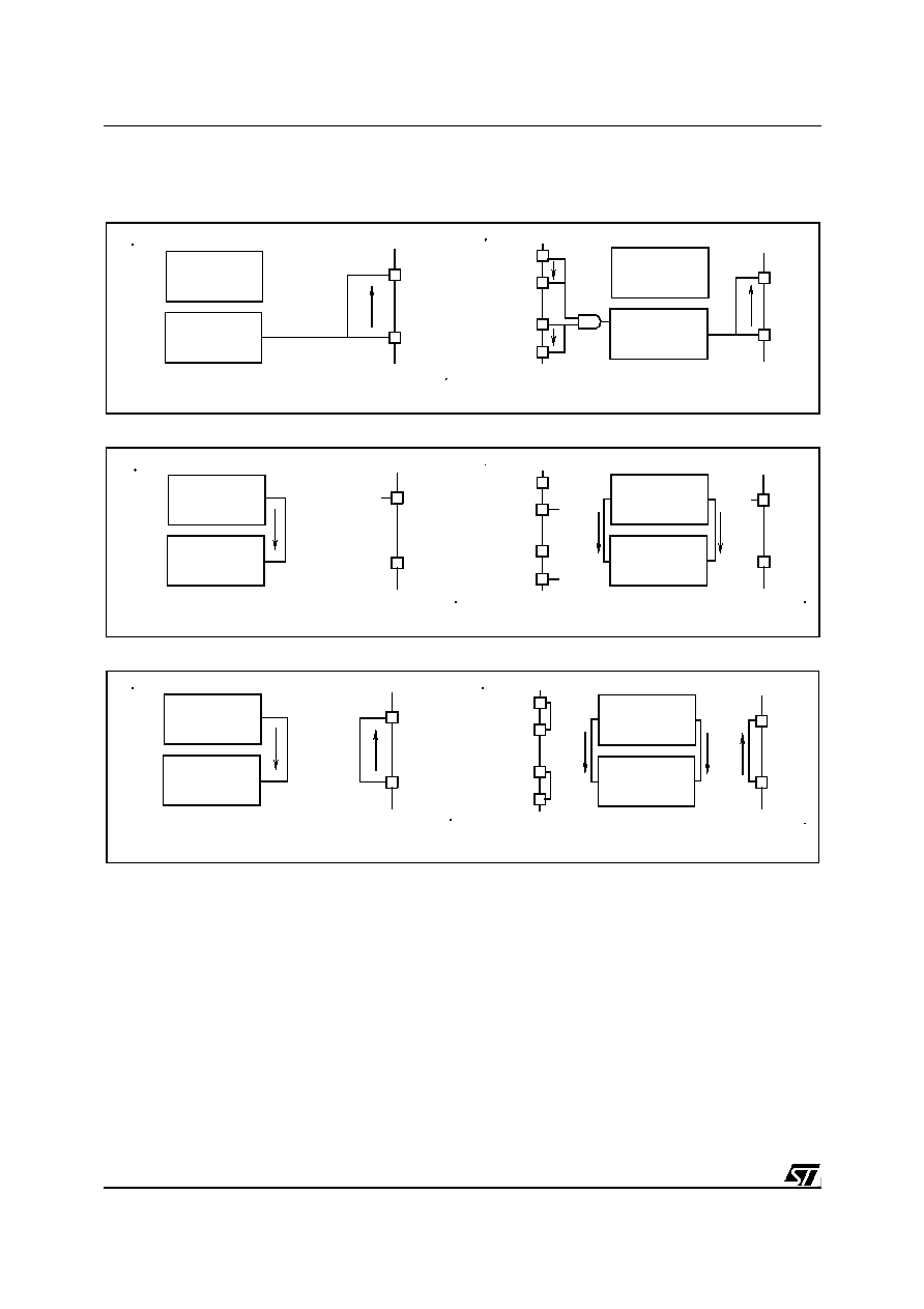
160/230
ST92163 - MULTIPROTOCOL SERIAL COMMUNICATIONS INTERFACE (SCI-M)
MULTIPROTOCOL SERIAL COMMUNICATIONS INTERFACE (Cont'd)
Figure 79. Auto Echo Configuration
Figure 80. Loop Back Configuration
Figure 81. Auto Echo and Loop-Back Configuration
All modes except Synchronous
Synchronous mode (SMEN=1)
RECEIVER
SIN
SOUT
VR000210
TRANSMITTER
RECEIVER
SIN
SOUT
VR00210A
TRANSMITTER
DCD
RTS
RXCLK
CLKOUT
All modes except Synchronous
Synchronous mode (SMEN=1)
RECEIVER
SIN
SOUT
VR000211
TRANSMITTER
LOGICAL 1
RECEIVER
SIN
SOUT
VR00211A
TRANSMITTER
DCD
RTS
RXCLK
CLKOUT
stand-by
value
stand-by
value
stand-by
value
clock
data
All modes except Synchronous
Synchronous mode (SMEN=1)
RECEIVER
SIN
SOUT
VR000212
TRANSMITTER
RECEIVER
SIN
SOUT
VR00212A
TRANSMITTER
DCD
RTS
RXCLK
CLKOUT
clock
data
161/230
ST92163 - MULTIPROTOCOL SERIAL COMMUNICATIONS INTERFACE (SCI-M)
MULTIPROTOCOL SERIAL COMMUNICATIONS INTERFACE (Cont'd)
8.4.6 Clocks And Serial Transmission Rates
The communication bit rate of the SCI transmitter
and receiver sections can be provided from the in-
ternal Baud Rate Generator or from external
sources. The bit rate clock is divided by 16 in
Asynchronous mode (CD in CCR reset), or undi-
vided in the 3 other modes (CD set).
With INTCLK running at 24MHz and no external
Clock provided, a maximum bit rate of 3MBaud
and 750KBaud is available in undivided and divide
by-16-mode respectively.
With INTCLK running at 24MHz and an external
Clock provided through the RXCLK/TXCLK lines,
a maximum bit rate of 3MBaud and 375KBaud is
available in undivided and divided by 16 mode re-
spectively (see
Figure 83
).
External Clock Sources. The External Clock in-
put pin TXCLK may be programmed by the XTCLK
and OCLK bits in the CCR register as: the transmit
clock input, Baud Rate Generator output (allowing
an external divider circuit to provide the receive
clock for split rate transmit and receive), or as
CLKOUT output in Synchronous and Serial Ex-
pansion modes. The RXCLK Receive clock input
is enabled by the XRX bit, this input should be set
in accordance with the setting of the CD bit.
Baud Rate Generator. The internal Baud Rate
Generator consists of a 16-bit programmable di-
vide by "N" counter which can be used to generate
the transmitter and/or receiver clocks. The mini-
mum baud rate divisor is 2 and the maximum divi-
sor is 2
16
-1. After initialising the baud rate genera-
tor, the divisor value is immediately loaded into the
counter. This prevents potentially long random
counts on the initial load.
The Baud Rate generator frequency is equal to the
Input Clock frequency divided by the Divisor value.
WARNING: Programming the baud rate divider to
0 or 1 will stop the divider.
The output of the Baud Rate generator has a pre-
cise 50% duty cycle. The Baud Rate generator can
use INTCLK for the input clock source. In this
case, INTCLK (and therefore the MCU Xtal)
should be chosen to provide a suitable frequency
for division by the Baud Rate Generator to give the
required transmit and receive bit rates. Suitable
INTCLK frequencies and the respective divider
values for standard Baud rates are shown in
Table
34
.
8.4.7 SCI -M Initialization Procedure
Writing to either of the two Baud Rate Generator
Registers immediately disables and resets the SCI
baud rate generator, as well as the transmitter and
receiver circuitry.
After writing to the second Baud Rate Generator
Register, the transmitter and receiver circuits are
enabled. The Baud Rate Generator will load the
new value and start counting.
To initialize the SCI, the user should first initialize
the most significant byte of the Baud Rate Gener-
ator Register; this will reset all SCI circuitry. The
user should then initialize all other SCI registers
(SICR/SOCR included) for the desired operating
mode and then, to enable the SCI, he should ini-
tialize the least significant byte Baud Rate Gener-
ator Register.
'On-the-Fly' modifications of the control registers'
content during transmitter/receiver operations, al-
though possible, can corrupt data and produce un-
desirable spikes on the I/O lines (data, clock and
control). Furthermore, modifying the control regis-
ters' content without reinitialising the SCI circuitry
(during stand-by cycles, waiting to transmit or re-
ceive data) must be kept carefully under control by
software to avoid spurious data being transmitted
or received.
Note: For synchronous receive operation, the data
and receive clock must not exhibit significant skew
between clock and data. The received data and
clock are internally synchronized to INTCLK.
Figure 82. SCI-M Baud Rate Generator Initialization Sequence
SELECT SCI
WORKING MODE
LEAST SIGNIFICANT
BYTE INITIALIZATION
MOST SIGNIFICANT
BYTE INITIALIZATION
162/230
ST92163 - MULTIPROTOCOL SERIAL COMMUNICATIONS INTERFACE (SCI-M)
MULTIPROTOCOL SERIAL COMMUNICATIONS INTERFACE (Cont'd)
Table 34. SCI-M Baud Rate Generator Divider Values Example 1
Table 35. SCI-M Baud Rate Generator Divider Values Example 2
INTCLK: 19660.800 KHz
Baud
Rate
Clock
Factor
Desired Freq
(kHz)
Divisor
Actual
Baud
Rate
Actual Freq
(kHz)
Deviation
Dec
Hex
50.00
16 X
0.80000
24576
6000
50.00
0.80000
0.0000%
75.00
16 X
1.20000
16384
4000
75.00
1.20000
0.0000%
110.00
16 X
1.76000
11170
2BA2
110.01
1.76014
-0.00081%
300.00
16 X
4.80000
4096
1000
300.00
4.80000
0.0000%
600.00
16 X
9.60000
2048
800
600.00
9.60000
0.0000%
1200.00
16 X
19.20000
1024
400
1200.00
19.20000
0.0000%
2400.00
16 X
38.40000
512
200
2400.00
38.40000
0.0000%
4800.00
16 X
76.80000
256
100
4800.00
76.80000
0.0000%
9600.00
16 X
153.60000
128
80
9600.00
153.60000
0.0000%
19200.00
16 X
307.20000
64
40
19200.00
307.20000
0.0000%
38400.00
16 X
614.40000
32
20
38400.00
614.40000
0.0000%
76800.00
16 X
1228.80000
16
10
76800.00
1228.80000
0.0000%
INTCLK: 24576 KHz
Baud
Rate
Clock
Factor
Desired Freq
(kHz)
Divisor
Actual
Baud
Rate
Actual Freq
(kHz)
Deviation
Dec
Hex
50.00
16 X
0.80000
30720
7800
50.00
0.80000
0.0000%
75.00
16 X
1.20000
20480
5000
75.00
1.20000
0.0000%
110.00
16 X
1.76000
13963
383B
110.01
1.76014
-0.00046%
300.00
16 X
4.80000
5120
1400
300.00
4.80000
0.0000%
600.00
16 X
9.60000
2560
A00
600.00
9.60000
0.0000%
1200.00
16 X
19.20000
1280
500
1200.00
19.20000
0.0000%
2400.00
16 X
38.40000
640
280
2400.00
38.40000
0.0000%
4800.00
16 X
76.80000
320
140
4800.00
76.80000
0.0000%
9600.00
16 X
153.60000
160
A0
9600.00
153.60000
0.0000%
19200.00
16 X
307.20000
80
50
19200.00
307.20000
0.0000%
38400.00
16 X
614.40000
40
28
38400.00
614.40000
0.0000%
76800.00
16 X
1228.80000
20
14
76800.00
1228.80000
0.0000%
163/230
ST92163 - MULTIPROTOCOL SERIAL COMMUNICATIONS INTERFACE (SCI-M)
MULTIPROTOCOL SERIAL COMMUNICATIONS INTERFACE (Cont'd)
8.4.8 Input Signals
SIN: Serial Data Input. This pin is the serial data
input to the SCI receiver shift register.
TXCLK: External Transmitter Clock Input. This
pin is the external input clock driving the SCI trans-
mitter. The TXCLK frequency must be greater than
or equal to 16 times the transmitter data rate (de-
pending whether the X16 or the X1 clock have
been selected). A 50% duty cycle is required for
this input and must have a period of at least twice
INTCLK. The use of the TXCLK pin is optional.
RXCLK: External Receiver Clock Input. This in-
put is the clock to the SCI receiver when using an
external clock source connected to the baud rate
generator. INTCLK is normally the clock source. A
50% duty cycle is required for this input and must
have a period of at least twice INTCLK. Use of RX-
CLK is optional.
DCD: Data Carrier Detect. This input is enabled
only in Synchronous mode; it works as a gate for
the RXCLK clock and informs the MCU that an
emitting device is transmitting a synchronous
frame. The active level can be programmed as 1
or 0 and must be provided at least one INTCLK pe-
riod before the first active edge of the input clock.
8.4.9 Output Signals
SOUT: Serial Data Output. This Alternate Func-
tion output signal is the serial data output for the
SCI transmitter in all operating modes.
CLKOUT: Clock Output. The alternate Function
of this pin outputs either the data clock from the
transmitter in Serial Expansion or Synchronous
modes, or the clock output from the Baud Rate
Generator. In Serial expansion mode it will clock
only the data portion of the frame and its stand-by
state is high: data is valid on the rising edge of the
clock. Even in Synchronous mode CLKOUT will
only clock the data portion of the frame, but the
stand-by level and active edge polarity are pro-
grammable by the user.
When Synchronous mode is disabled (SMEN in
SICR is reset), the state of the XTCLK and OCLK
bits in CCR determine the source of CLKOUT; '11'
enables the Serial Expansion Mode.
When the Synchronous mode is enabled (SMEN
in SICR is set), the state of the XTCLK and OCLK
bits in CCR determine the source of CLKOUT; '00'
disables it for PLM applications.
RTS: Request To Send. This output Alternate
Function is only enabled in Synchronous mode; it
becomes active when the Least Significant Bit of
the data frame is sent to the Serial Output Pin
(SOUT) and indicates to the target device that the
MCU is about to send a synchronous frame; it re-
turns to its stand-by value just after the last active
edge of CLKOUT (MSB transmitted). The active
level can be programmed high or low.
SDS: Synchronous Data Strobe. This output Al-
ternate function is only enabled in Synchronous
mode; it becomes active high when the Least Sig-
nificant Bit is sent to the Serial Output Pins
(SOUT) and indicates to the target device that the
MCU is about to send the first bit for each synchro-
nous frame. It is active high on the first bit and it is
low for all the rest of the frame. The active level
can not be programmed.
Figure 83. Receiver and Transmitter Clock Frequencies
Note: The internal receiver and transmitter clocks
are the ones applied to the Tx and Rx shift regis-
ters (see
Figure 74
).
Min Max
Conditions
Receiver Clock Frequency
External RXCLK
0
INTCLK/8
1x mode
0
INTCLK/4
16x mode
Internal Receiver Clock
0
INTCLK/8
1x mode
0
INTCLK/2
16x mode
Transmitter Clock Frequency
External TXCLK
0
INTCLK/8
1x mode
0
INTCLK/4
16x mode
Internal Transmitter Clock
0
INTCLK/8
1x mode
0
INTCLK/2
16x mode

164/230
ST92163 - MULTIPROTOCOL SERIAL COMMUNICATIONS INTERFACE (SCI-M)
MULTIPROTOCOL SERIAL COMMUNICATIONS INTERFACE (Cont'd)
8.4.10 Interrupts and DMA
8.4.10.1 Interrupts
The SCI can generate interrupts as a result of sev-
eral conditions. Receiver interrupts include data
pending, receive errors (overrun, framing and par-
ity), as well as address or break pending. Trans-
mitter interrupts are software selectable for either
Transmit Buffer Register Empty (BSN set) or for
Transmit Shift Register Empty (BSN reset) condi-
tions.
Typical usage of the Interrupts generated by the
SCI peripheral are illustrated in
Figure 84
.
The SCI peripheral is able to generate interrupt re-
quests as a result of a number of events, several
of which share the same interrupt vector. It is
therefore necessary to poll S_ISR, the Interrupt
Status Register, in order to determine the active
trigger. These bits should be reset by the program-
mer during the Interrupt Service routine.
The four major levels of interrupt are encoded in
hardware to provide two bits of the interrupt vector
register, allowing the position of the block of point-
er vectors to be resolved to an 8 byte block size.
The SCI interrupts have an internal priority struc-
ture in order to resolve simultaneous events. Refer
also to Section 8.4.4 for more details relating to
Synchronous mode.
Table 36. SCI Interrupt Internal Priority
Receive DMA Request
Highest Priority
Transmit DMA Request
Receive Interrupt
Transmit Interrupt
Lowest Priority
165/230
ST92163 - MULTIPROTOCOL SERIAL COMMUNICATIONS INTERFACE (SCI-M)
MULTIPROTOCOL SERIAL COMMUNICATIONS INTERFACE (Cont'd)
Table 37. SCI-M Interrupt Vectors
Figure 84. SCI-M Interrupts: Example of Typical Usage
Interrupt Source
Vector Address
Transmitter Buffer or Shift Register Empty
Transmit DMA end of Block
xxx x110
Received Data Pending
Receive DMA end of Block
xxxx x100
Break Detector
Address Word Match
xxxx x010
Receiver Error
xxxx x000
INTERRUPT
BREAK
MATCH
ADDRESS
DATA
ADDRESS AFTER BREAK CONDITION
ADDRESS WORD MARKED BY D9=1
ADDRESS
INTERRUPT
INTERRUPT
D9=1
D9 ACTING AS DATA CONTROL WITH SEPARATE INTERRUPT
CHARACTER SEARCH MODE
INTERRUPT
VA00270
BREAK
BREAK
INTERRUPT
DATA
INTERRUPT
DATA
INTERRUPT
DATA
INTERRUPT
DATA
INTERRUPT
DATA
INTERRUPT
DATA
INTERRUPT
DATA
INTERRUPT
DATA
INTERRUPT
DATA
INTERRUPT
DATA
INTERRUPT
DATA
INTERRUPT
DATA
INTERRUPT
DATA
INTERRUPT
DATA
INTERRUPT
DATA
INTERRUPT
INTERRUPT
INTERRUPT
DATA
ADDRESS
DATA
DATA
DATA
DATA
NO MATCH
ADDRESS
BREAK
DATA
NO MATCH
ADDRESS
MATCH
DATA
DATA
DATA
MATCH
DATA
CHAR MATCH
DATA
DATA
DATA
DATA
ADDRESS
DATA
DATA
D9=1
DATA
DATA
DATA
DATA

166/230
ST92163 - MULTIPROTOCOL SERIAL COMMUNICATIONS INTERFACE (SCI-M)
MULTIPROTOCOL SERIAL COMMUNICATIONS INTERFACE (Cont'd)
8.4.10.2 DMA
Two DMA channels are associated with the SCI,
for transmit and for receive. These follow the reg-
ister scheme as described in the DMA chapter.
DMA Reception
To perform a DMA transfer in reception mode:
1. Initialize the DMA counter (RDCPR) and DMA
address (RDAPR) registers
2. Enable DMA by setting the RXD bit in the IDPR
register.
3. DMA transfer is started when data is received
by the SCI.
DMA Transmission
To perform a DMA transfer in transmission mode:
1. Initialize the DMA counter (TDCPR) and DMA
address (TDAPR) registers.
2. Enable DMA by setting the TXD bit in the IDPR
register.
3. DMA transfer is started by writing a byte in the
Transmitter Buffer register (TXBR).
If this byte is the first data byte to be transmitted,
the DMA counter and address registers must be
initialized to begin DMA transmission at the sec-
ond byte. Alternatively, DMA transfer can be start-
ed by writing a dummy byte in the TXBR register.
DMA Interrupts
When DMA is active, the Received Data Pending
and the Transmitter Shift Register Empty interrupt
sources are replaced by the DMA End Of Block re-
ceive and transmit interrupt sources.
Note: To handle DMA transfer correctly in trans-
mission, the BSN bit in the IMR register must be
cleared. This selects the Transmitter Shift Register
Empty event as the DMA interrupt source.
The transfer of the last byte of a DMA data block
will be followed by a DMA End Of Block transmit or
receive interrupt, setting the TXEOB or RXEOB
bit.
A typical Transmission End Of Block interrupt rou-
tine will perform the following actions:
1. Restore the DMA counter register (TDCPR).
2. Restore the DMA address register (TDAPR).
3. Clear the Transmitter Shift Register Empty bit
TXSEM in the S_ISR register to avoid spurious
interrupts.
4. Clear the Transmitter End Of Block (TXEOB)
pending bit in the IMR register.
5. Set the TXD bit in the IDPR register to enable
DMA.
6. Load the Transmitter Buffer Register (TXBR)
with the next byte to transmit.
The above procedure handles the case where a
further DMA transfer is to be performed.
Error Interrupt Handling
If an error interrupt occurs while DMA is enabled in
reception mode, DMA transfer is stopped.
To resume DMA transfer, the error interrupt han-
dling routine must clear the corresponding error
flag. In the case of an Overrun error, the routine
must also read the RXBR register.
Character Search Mode with DMA
In Character Search Mode with DMA, when a
character match occurs, this character is not trans-
ferred. DMA continues with the next received char-
acter. To avoid an Overrun error occurring, the
Character Match interrupt service routine must
read the RXBR register.

167/230
ST92163 - MULTIPROTOCOL SERIAL COMMUNICATIONS INTERFACE (SCI-M)
MULTIPROTOCOL SERIAL COMMUNICATIONS INTERFACE (Cont'd)
8.4.11 Register Description
The SCI-M registers are located in the following
pages in the ST9:
SCI-M number 0: page 24 (18h)
SCI-M number 1: page 25 (19h) (when present)
The SCI is controlled by the following registers:
Address
Register
R240 (F0h)
Receiver DMA Transaction Counter Pointer Register
R241 (F1h)
Receiver DMA Source Address Pointer Register
R242 (F2h)
Transmitter DMA Transaction Counter Pointer Register
R243 (F3h)
Transmitter DMA Destination Address Pointer Register
R244 (F4h)
Interrupt Vector Register
R245 (F5h)
Address Compare Register
R246 (F6h)
Interrupt Mask Register
R247 (F7h)
Interrupt Status Register
R248 (F8h)
Receive Buffer Register same Address as Transmitter Buffer Register (Read Only)
R248 (F8h)
Transmitter Buffer Register same Address as Receive Buffer Register (Write only)
R249 (F9h)
Interrupt/DMA Priority Register
R250 (FAh)
Character Configuration Register
R251 (FBh)
Clock Configuration Register
R252 (FCh)
Baud Rate Generator High Register
R253 (FDh)
Baud Rate Generator Low Register
R254 (FEh)
Synchronous Input Control Register
R255 (FFh)
Synchronous Output Control Register
168/230
ST92163 - MULTIPROTOCOL SERIAL COMMUNICATIONS INTERFACE (SCI-M)
MULTIPROTOCOL SERIAL COMMUNICATIONS INTERFACE (Cont'd)
RECEIVER DMA COUNTER POINTER (RDCPR)
R240 - Read/Write
Reset value: undefined
Bit 7:1 = RC[7:1]:
Receiver DMA Counter Pointer.
These bits contain the address of the receiver
DMA transaction counter in the Register File.
Bit 0 = RR/M:
Receiver Register File/Memory Se-
lector
.
0: Select Memory space as destination.
1: Select the Register File as destination.
RECEIVER DMA ADDRESS POINTER (RDAPR)
R241 - Read/Write
Reset value: undefined
Bit 7:1 = RA[7:1]:
Receiver DMA Address Pointer.
These bits contain the address of the pointer (in
the Register File) of the receiver DMA data source.
Bit 0 = RPS:
Receiver DMA Memory Pointer Se-
lector.
This bit is only significant if memory has been se-
lected for DMA transfers (RR/M = 0 in the RDCPR
register).
0: Select ISR register for receiver DMA transfers
address extension.
1: Select DMASR register for receiver DMA trans-
fers address extension.
TRANSMITTER DMA COUNTER POINTER
(TDCPR)
R242 - Read/Write
Reset value: undefined
Bit 7:1 = TC[7:1]:
Transmitter DMA Counter Point-
er
.
These bits contain the address of the transmitter
DMA transaction counter in the Register File.
Bit 0 = TR/M:
Transmitter Register File/Memory
Selector
.
0: Select Memory space as source.
1: Select the Register File as source.
TRANSMITTER DMA ADDRESS POINTER
(TDAPR)
R243 - Read/Write
Reset value: undefined
Bit 7:1 = TA[7:1]:
Transmitter DMA Address Point-
er.
These bits contain the address of the pointer (in
the Register File) of the transmitter DMA data
source.
Bit 0 = TPS:
Transmitter DMA Memory Pointer Se-
lector.
This bit is only significant if memory has been se-
lected for DMA transfers (TR/M = 0 in the TDCPR
register).
0: Select ISR register for transmitter DMA transfers
address extension.
1: Select DMASR register for transmitter DMA
transfers address extension.
7
0
RC7
RC6
RC5
RC4
RC3
RC2
RC1
RR/M
7
0
RA7
RA6
RA5
RA4
RA3
RA2
RA1
RPS
7
0
TC7
TC6
TC5
TC4
TC3
TC2
TC1
TR/M
7
0
TA7
TA6
TA5
TA4
TA3
TA2
TA1
TPS
169/230
ST92163 - MULTIPROTOCOL SERIAL COMMUNICATIONS INTERFACE (SCI-M)
MULTIPROTOCOL SERIAL COMMUNICATIONS INTERFACE (Cont'd)
INTERRUPT VECTOR REGISTER (S_IVR)
R244 - Read/Write
Reset value: undefined
Bit 7:3 = V[7:3]:
SCI Interrupt Vector Base Ad-
dress.
User programmable interrupt vector bits for trans-
mitter and receiver.
Bit 2:1 = EV[2:1]:
Encoded Interrupt Source.
Both bits EV2 and EV1 are read only and set by
hardware according to the interrupt source.
Bit 0 = D0: This bit is forced by hardware to 0.
ADDRESS/DATA COMPARE REGISTER (ACR)
R245 - Read/Write
Reset value: undefined
Bit 7:0 = AC[7:0]:
Address/Compare Character
.
With either 9th bit address mode, address after
break mode, or character search, the received ad-
dress will be compared to the value stored in this
register. When a valid address matches this regis-
ter content, the Receiver Address Pending bit
(RXAP in the S_ISR register) is set. After the
RXAP bit is set in an addressed mode, all received
data words will be transferred to the Receiver Buff-
er Register.
7
0
V7
V6
V5
V4
V3
EV2
EV1
0
EV2 EV1
Interrupt source
0
0
Receiver Error (Overrun, Framing, Parity)
0
1
Break Detect or Address Match
1
0
Received Data Pending/Receiver DMA
End of Block
1
1
Transmitter buffer or shift register empty
transmitter DMA End of Block
7
0
AC7
AC6
AC5
AC4
AC3
AC2
AC1
AC0

170/230
ST92163 - MULTIPROTOCOL SERIAL COMMUNICATIONS INTERFACE (SCI-M)
MULTIPROTOCOL SERIAL COMMUNICATIONS INTERFACE (Cont'd)
INTERRUPT MASK REGISTER (IMR)
R246 - Read/Write
Reset value: 0xx00000
Bit 7 = BSN:
Buffer or shift register empty inter-
rupt
.
This bit selects the source of the transmitter regis-
ter empty interrupt.
0: Select a Shift Register Empty as source of a
Transmitter Register Empty interrupt.
1: Select a Buffer Register Empty as source of a
Transmitter Register Empty interrupt.
Bit 6 = RXEOB:
Received End of Block.
This bit is set by hardware only and must be reset
by software. RXEOB is set after a receiver DMA
cycle to mark the end of a data block.
0: Clear the interrupt request.
1: Mark the end of a received block of data.
Bit 5 = TXEOB:
Transmitter End of Block.
This bit is set by hardware only and must be reset
by software. TXEOB is set after a transmitter DMA
cycle to mark the end of a data block.
0: Clear the interrupt request.
1: Mark the end of a transmitted block of data.
Bit 4 = RXE:
Receiver Error Mask.
0: Disable Receiver error interrupts (OE, PE, and
FE pending bits in the S_ISR register).
1: Enable Receiver error interrupts.
Bit 3 = RXA:
Receiver Address Mask
.
0: Disable Receiver Address interrupt (RXAP
pending bit in the S_ISR register).
1: Enable Receiver Address interrupt.
Bit 2 = RXB:
Receiver Break Mask
.
0: Disable Receiver Break interrupt (RXBP pend-
ing bit in the S_ISR register).
1: Enable Receiver Break interrupt.
Bit 1 = RXDI:
Receiver Data Interrupt Mask
.
0: Disable Receiver Data Pending and Receiver
End of Block interrupts (RXDP and RXEOB
pending bits in the S_ISR register).
1: Enable Receiver Data Pending and Receiver
End of Block interrupts.
Note: RXDI has no effect on DMA transfers.
Bit 0 = TXDI:
Transmitter Data Interrupt Mask
.
0: Disable Transmitter Buffer Register Empty,
Transmitter Shift Register Empty, or Transmitter
End of Block interrupts (TXBEM, TXSEM, and
TXEOB bits in the S_ISR register).
1: Enable Transmitter Buffer Register Empty,
Transmitter Shift Register Empty, or Transmitter
End of Block interrupts.
Note: TXDI has no effect on DMA transfers.
7
0
BSN
RXEOB TXEOB
RXE
RXA
RXB
RXDI
TXDI

171/230
ST92163 - MULTIPROTOCOL SERIAL COMMUNICATIONS INTERFACE (SCI-M)
MULTIPROTOCOL SERIAL COMMUNICATIONS INTERFACE (Cont'd)
INTERRUPT STATUS REGISTER (S_ISR)
R247 - Read/Write
Reset value: undefined
Bit 7 = OE:
Overrun Error Pending
.
This bit is set by hardware if the data in the Receiv-
er Buffer Register was not read by the CPU before
the next character was transferred into the Receiv-
er Buffer Register (the previous data is lost).
0: No Overrun Error.
1: Overrun Error occurred.
Bit 6 = FE:
Framing Error Pending bit
.
This bit is set by hardware if the received data
word did not have a valid stop bit.
0: No Framing Error.
1: Framing Error occurred.
Note: In the case where a framing error occurs
when the SCI is programmed in address mode
and is monitoring an address, the interrupt is as-
serted and the corrupted data element is trans-
ferred to the Receiver Buffer Register.
Bit 5 = PE:
Parity Error Pending
.
This bit is set by hardware if the received word did
not have the correct even or odd parity bit.
0: No Parity Error.
1: Parity Error occurred.
Bit 4 = RXAP:
Receiver Address Pending
.
RXAP is set by hardware after an interrupt ac-
knowledged in the address mode.
0: No interrupt in address mode.
1: Interrupt in address mode occurred.
Note: The source of this interrupt is given by the
couple of bits (AMEN, AM) as detailed in the IDPR
register description.
Bit 3 = RXBP:
Receiver Break Pending bit
.
This bit is set by hardware if the received data in-
put is held low for the full word transmission time
(start bit, data bits, parity bit, stop bit).
0: No break received.
1: Break event occurred.
Bit 2 = RXDP:
Receiver Data Pending bit.
This bit is set by hardware when data is loaded
into the Receiver Buffer Register.
0: No data received.
1: Data received in Receiver Buffer Register.
Bit 1 = TXBEM:
Transmitter Buffer Register Emp-
ty
.
This bit is set by hardware if the Buffer Register is
empty.
0: No Buffer Register Empty event.
1: Buffer Register Empty.
Bit 0 = TXSEM:
Transmitter Shift Register Empty
.
This bit is set by hardware if the Shift Register has
completed the transmission of the available data.
0: No Shift Register Empty event.
1: Shift Register Empty.
Note: The Interrupt Status Register bits can be re-
set but cannot be set by the user. The interrupt
source must be cleared by resetting the related bit
when executing the interrupt service routine (natu-
rally the other pending bits should not be reset).
7
0
OE
FE
PE
RXAP
RXBP RXDP
TXBEM
TXSEM

172/230
ST92163 - MULTIPROTOCOL SERIAL COMMUNICATIONS INTERFACE (SCI-M)
MULTIPROTOCOL SERIAL COMMUNICATIONS INTERFACE (Cont'd)
RECEIVER BUFFER REGISTER (RXBR)
R248 - Read only
Reset value: undefined
Bit 7:0 = RD[7:0]:
Received Data.
This register stores the data portion of the re-
ceived word. The data will be transferred from the
Receiver Shift Register into the Receiver Buffer
Register at the end of the word. All receiver inter-
rupt conditions will be updated at the time of trans-
fer. If the selected character format is less than 8
bits, unused most significant bits will forced to "1".
Note: RXBR and TXBR are two physically differ-
ent registers located at the same address.
TRANSMITTER BUFFER REGISTER (TXBR)
R248 - Write only
Reset value: undefined
Bit 7:0 = TD[7:0]:
Transmit Data
.
The ST9 core will load the data for transmission
into this register. The SCI will transfer the data
from the buffer into the Shift Register when availa-
ble. At the transfer, the Transmitter Buffer Register
interrupt is updated. If the selected word format is
less than 8 bits, the unused most significant bits
are not significant.
Note: TXBR and RXBR are two physically differ-
ent registers located at the same address.
7
0
RD7
RD6
RD5
RD4
RD3
RD2
RD1
RD0
7
0
TD7
TD6
TD5
TD4
TD3
TD2
TD1
TD0
173/230
ST92163 - MULTIPROTOCOL SERIAL COMMUNICATIONS INTERFACE (SCI-M)
MULTIPROTOCOL SERIAL COMMUNICATIONS INTERFACE (Cont'd)
INTERRUPT/DMA PRIORITY REGISTER (IDPR)
R249 - Read/Write
Reset value: undefined
Bit 7 = AMEN:
Address Mode Enable.
This bit, together with the AM bit (in the CHCR reg-
ister), decodes the desired addressing/9th data
bit/character match operation.
In Address mode the SCI monitors the input serial
data until its address is detected
Note: Upon reception of address, the RXAP bit (in
the Interrupt Status Register) is set and an inter-
rupt cycle can begin. The address character will
not be transferred into the Receiver Buffer Regis-
ter but all data following the matched SCI address
and preceding the next address word will be trans-
ferred to the Receiver Buffer Register and the
proper interrupts updated. If the address does not
match, all data following this unmatched address
will not be transferred to the Receiver Buffer Reg-
ister.
In any of the cases the RXAP bit must be reset by
software before the next word is transferred into
the Buffer Register.
When AMEN is reset and AM is set, a useful char-
acter search function is performed. This allows the
SCI to generate an interrupt whenever a specific
character is encountered (e.g. Carriage Return).
Bit 6 = SB:
Set Break
.
0: Stop the break transmission after minimum
break length.
1: Transmit a break following the transmission of all
data in the Transmitter Shift Register and the
Buffer Register.
Note: The break will be a low level on the transmit-
ter data output for at least one complete word for-
mat. If software does not reset SB before the min-
imum break length has finished, the break condi-
tion will continue until software resets SB. The SCI
terminates the break condition with a high level on
the transmitter data output for one transmission
clock period.
Bit 5 = SA:
Set Address
.
If an address/9th data bit mode is selected, SA val-
ue will be loaded for transmission into the Shift
Register. This bit is cleared by hardware after its
load.
0: Indicate it is not an address word.
1: Indicate an address word.
Note: Proper procedure would be, when the
Transmitter Buffer Register is empty, to load the
value of SA and then load the data into the Trans-
mitter Buffer Register.
Bit 4 = RXD:
Receiver DMA Mask
.
This bit is reset by hardware when the transaction
counter value decrements to zero. At that time a
receiver End of Block interrupt can occur.
0: Disable Receiver DMA request (the RXDP bit in
the S_ISR register can request an interrupt).
1: Enable Receiver DMA request (the RXDP bit in
the S_ISR register can request a DMA transfer).
Bit 3 = TXD:
Transmitter DMA Mask
.
This bit is reset by hardware when the transaction
counter value decrements to zero. At that time a
transmitter End Of Block interrupt can occur.
0: Disable Transmitter DMA request (TXBEM or
TXSEM bits in S_ISR can request an interrupt).
1: Enable Transmitter DMA request (TXBEM or
TXSEM bits in S_ISR can request a DMA trans-
fer).
Bit 2:0 = PRL[2:0]:
SCI Interrupt/DMA Priority bits
.
The priority for the SCI is encoded with
(PRL2,PRL1,PRL0). Priority level 0 is the highest,
while level 7 represents no priority.
When the user has defined a priority level for the
SCI, priorities within the SCI are hardware defined.
These SCI internal priorities are:
7
0
AMEN
SB
SA
RXD
TXD
PRL2
PRL1
PRL0
AMEN
AM
0
0
Address interrupt if 9th data bit = 1
0
1
Address interrupt if character match
1
0
Address interrupt if character match
and 9th data bit =1
1
1
Address interrupt if character match
with word immediately following Break
Receiver DMA request
highest priority
Transmitter DMA request
Receiver interrupt
Transmitter interrupt
lowest priority
174/230
ST92163 - MULTIPROTOCOL SERIAL COMMUNICATIONS INTERFACE (SCI-M)
MULTIPROTOCOL SERIAL COMMUNICATIONS INTERFACE (Cont'd)
CHARACTER CONFIGURATION REGISTER
(CHCR)
R250 - Read/Write
Reset value: undefined
Bit 7 = AM:
Address Mode
.
This bit, together with the AMEN bit (in the IDPR
register), decodes the desired addressing/9th data
bit/character match operation. Please refer to the
table in the IDPR register description.
Bit 6 = EP:
Even Parity
.
0: Select odd parity (when parity is enabled).
1: Select even parity (when parity is enabled).
Bit 5 = PEN:
Parity Enable
.
0: No parity bit.
1: Parity bit generated (transmit data) or checked
(received data).
Note: If the address/9th bit is enabled, the parity
bit will precede the address/9th bit (the 9th bit is
never included in the parity calculation).
Bit 4 = AB:
Address/9th Bit
.
0: No Address/9th bit.
1: Address/9th bit included in the character format
between the parity bit and the first stop bit. This
bit can be used to address the SCI or as a ninth
data bit.
Bit 3:2 = SB[1:0]:
Number of
Stop Bits
..
Bit 1:0 = WL[1:0]:
Number of Data Bits
7
0
AM
EP
PEN
AB
SB1
SB0
WL1
WL0
SB1
SB0
Number of stop bits
in 16X mode
in 1X mode
0
0
1
1
0
1
1.5
2
1
0
2
2
1
1
2.5
3
WL1
WL0
Data Length
0
0
5 bits
0
1
6 bits
1
0
7 bits
1
1
8 bits
175/230
ST92163 - MULTIPROTOCOL SERIAL COMMUNICATIONS INTERFACE (SCI-M)
MULTIPROTOCOL SERIAL COMMUNICATIONS INTERFACE (Cont'd)
CLOCK CONFIGURATION REGISTER (CCR)
R251 - Read/Write
Reset value: 0000 0000 (00h)
Bit 7 = XTCLK
This bit, together with the OCLK bit, selects the
source for the transmitter clock. The following ta-
ble shows the coding of XTCLK and OCLK.
Bit 6 = OCLK
This bit, together with the XTCLK bit, selects the
source for the transmitter clock. The following ta-
ble shows the coding of XTCLK and OCLK.
Bit 5 = XRX:
External Receiver Clock Source
.
0: External receiver clock source not used.
1: Select the external receiver clock source.
Note: The external receiver clock frequency must
be 16 times the data rate, or equal to the data rate,
depending on the status of the CD bit.
Bit 4 = XBRG:
Baud Rate Generator Clock
Source
.
0: Select INTCLK for the baud rate generator.
1: Select the external receiver clock for the baud
rate generator.
Bit 3 = CD:
Clock Divisor
.
The status of CD will determine the SCI configura-
tion (synchronous/asynchronous).
0: Select 16X clock mode for both receiver and
transmitter.
1: Select 1X clock mode for both receiver and
transmitter.
Note: In 1X clock mode, the transmitter will trans-
mit data at one data bit per clock period. In 16X
mode each data bit period will be 16 clock periods
long.
Bit 2 = AEN:
Auto Echo Enable
.
0: No auto echo mode.
1: Put the SCI in auto echo mode.
Note: Auto Echo mode has the following effect:
the SCI transmitter is disconnected from the data-
out pin SOUT, which is driven directly by the re-
ceiver data-in pin, SIN. The receiver remains con-
nected to SIN and is operational, unless loopback
mode is also selected.
Bit 1 = LBEN:
Loopback Enable
.
0: No loopback mode.
1: Put the SCI in loopback mode.
Note: In this mode, the transmitter output is set to
a high level, the receiver input is disconnected,
and the output of the Transmitter Shift Register is
looped back into the Receiver Shift Register input.
All interrupt sources (transmitter and receiver) are
operational.
Bit 0 = STPEN:
Stick Parity Enable
.
0: The transmitter and the receiver will follow the
parity of even parity bit EP in the CHCR register.
1: The transmitter and the receiver will use the op-
posite parity type selected by the even parity bit
EP in the CHCR register.
7
0
XTCLK
OCLK
XRX
XBRG
CD
AEN
LBEN
STPEN
XTCLK
OCLK
Pin Function
0
0
Pin is used as a general I/O
0
1
Pin = TXCLK (used as an input)
1
0
Pin = CLKOUT (outputs the Baud
Rate Generator clock)
1
1
Pin = CLKOUT (outputs the Serial
expansion and synchronous
mode clock)
EP
SPEN
Parity (Transmitter &
Receiver)
0 (odd)
0
Odd
1 (even)
0
Even
0 (odd)
1
Even
1 (even)
1
Odd
176/230
ST92163 - MULTIPROTOCOL SERIAL COMMUNICATIONS INTERFACE (SCI-M)
MULTIPROTOCOL SERIAL COMMUNICATIONS INTERFACE (Cont'd)
BAUD RATE GENERATOR HIGH REGISTER
(BRGHR)
R252 - Read/Write
Reset value: undefined
BAUD RATE GENERATOR LOW REGISTER
(BRGLR)
R253 - Read/Write
Reset value: undefined
Bit 15:0 =
Baud Rate Generator MSB and LSB.
The Baud Rate generator is a programmable di-
vide by "N" counter which can be used to generate
the clocks for the transmitter and/or receiver. This
counter divides the clock input by the value in the
Baud Rate Generator Register. The minimum
baud rate divisor is 2 and the maximum divisor is
2
16
-1. After initialization of the baud rate genera-
tor, the divisor value is immediately loaded into the
counter. This prevents potentially long random
counts on the initial load. If set to 0 or 1, the Baud
Rate Generator is stopped.
SYNCHRONOUS INPUT CONTROL (SICR)
R254 - Read/Write
Reset value: 0000 0011 (03h)
Bit 7 = SMEN:
Synchronous Mode Enable
.
0: Disable all features relating to Synchronous
mode (the contents of SICR and SOCR are ig-
nored).
1: Select Synchronous mode with its programmed
I/O configuration.
Bit 6 = INPL:
SIN Input Polarity
.
0: Polarity not inverted.
1: Polarity inverted.
Note: INPL only affects received data. In Auto-
Echo mode SOUT = SIN even if INPL is set. In
Loop-Back mode the state of the INPL bit is irrele-
vant.
Bit 5 = XCKPL:
Receiver Clock Polarity
.
0: RXCLK is active on the rising edge.
1: RXCLK is active on the falling edge.
Note: XCKPL only affects the receiver clock. In
Auto-Echo mode CLKOUT = RXCLK independ-
ently of the XCKPL status. In Loop-Back the state
of the XCKPL bit is irrelevant.
Bit 4 = DCDEN:
DCD Input Enable
.
0: Disable hardware synchronization.
1: Enable hardware synchronization.
Note: When DCDEN is set, RXCLK drives the re-
ceiver section only during the active level of the
DCD input (DCD works as a gate on RXCLK, in-
forming the MCU that a transmitting device is
sending a synchronous frame to it).
Bit 3 = DCDPL:
DCD Input Polarity
.
0: The DCD input is active when LOW.
1: The DCD input is active when HIGH.
Note: DCDPL only affects the gating activity of the
receiver clock. In Auto-Echo mode RTS = DCD in-
dependently of DCDPL. In Loop-Back mode, the
state of DCDPL is irrelevant.
Bit 2 = INPEN:
All Input Disable
.
0: Enable SIN/RXCLK/DCD inputs.
1: Disable SIN/RXCLK/DCD inputs.
Bit 1:0 = "Don't Care"
15
8
BG15
BG14
BG13
BG12
BG11
BG10
BG9
BG8
7
0
BG7
BG6
BG5
BG4
BG3
BG2
BG1
BG0
7
0
SMEN
INPL
XCKPL
DCDE
N
DCDP
L
INPEN
X
X

177/230
ST92163 - MULTIPROTOCOL SERIAL COMMUNICATIONS INTERFACE (SCI-M)
MULTIPROTOCOL SERIAL COMMUNICATIONS INTERFACE (Cont'd)
SYNCHRONOUS OUTPUT CONTROL (SOCR)
R255 - Read/Write
Reset value: 0000 0001 (01h)
Bit 7 = OUTPL:
SOUT Output Polarity.
0: Polarity not inverted.
1: Polarity inverted.
Note: OUTPL only affects the data sent by the
transmitter section. In Auto-Echo mode SOUT =
SIN even if OUTPL=1. In Loop-Back mode, the
state of OUTPL is irrelevant.
Bit 6 = OUTSB:
SOUT Output Stand-By Level
.
0: SOUT stand-by level is HIGH.
1: SOUT stand-by level is LOW.
Bit 5 = OCKPL:
Transmitter Clock Polarity.
0: CLKOUT is active on the rising edge.
1: CLKOUT is active on the falling edge.
Note: OCKPL only affects the transmitter clock. In
Auto-Echo mode CLKOUT = RXCLK independ-
ently of the state of OCKPL. In Loop-Back mode
the state of OCKPL is irrelevant.
Bit 4 = OCKSB:
Transmitter Clock Stand-By Lev-
el.
0: The CLKOUT stand-by level is HIGH.
1: The CLKOUT stand-by level is LOW.
Bit 3 = RTSEN:
RTS and SDS Output Enable
.
0: Disable the RTS and SDS hardware synchroni-
sation.
1: Enable the RTS and SDS hardware synchroni-
sation.
Notes:
≠ When RTSEN is set, the RTS output becomes
active just before the first active edge of CLK-
OUT and indicates to target device that the MCU
is about to send a synchronous frame; it returns
to its stand-by value just after the last active edge
of CLKOUT (MSB transmitted).
≠ When RTSEN is set, the SDS output becomes
active high and indicates to the target device that
the MCU is about to send the first bit of a syn-
chronous frame on the Serial Output Pin
(SOUT); it returns to low level as soon as the
second bit is sent on the Serial Output Pin
(SOUT). In this way a positive pulse is generated
each time that the first bit of a synchronous frame
is present on the Serial Output Pin (SOUT).
Bit 2 = RTSPL:
RTS Output Polarity.
0: The RTS output is active when LOW.
1: The RTS output is active when HIGH.
Note: RTSPL only affects the RTS activity on the
output pin. In Auto-Echo mode RTS = DCD inde-
pendently from the RTSPL value. In Loop-Back
mode RTSPL value is 'Don't Care'.
Bit 1 = OUTDIS:
Disable all outputs.
This feature is available on specific devices only
(see device pin-out description).
When OUTDIS=1, all output pins (if configured in
Alternate Function mode) will be put in High Im-
pedance for networking.
0: SOUT/CLKOUT/enabled
1: SOUT/CLKOUT/RTS put in high impedance
Bit 0 = "Don't Care"
7
0
OUTP
L
OUTS
B
OCKP
L
OCKS
B
RTSE
N
RTS
PL
OUT
DIS
X

178/230
ST92163 - I2C BUS INTERFACE
8.5 I
2
C BUS INTERFACE
8.5.1 Introduction
The I
2
C bus Interface serves as an interface be-
tween the microcontroller and the serial I
2
C bus. It
provides both multimaster and slave functions with
both 7-bit and 10-bit address modes; it controls all
I
2
C bus-specific sequencing, protocol, arbitration,
timing and supports both standard (100KHz) and
fast I
2
C modes (400KHz).
Using DMA, data can be transferred with minimum
use of CPU time.
The peripheral uses two external lines to perform
the protocols: SDA, SCL.
8.5.2 Main Features
s
Parallel-bus/I
2
C protocol converter
s
Multi-master capability
s
7-bit/10-bit Addressing
s
Standard I
2
C mode/Fast I
2
C mode
s
Transmitter/Receiver flag
s
End-of-byte transmission flag
s
Transfer problem detection
s
Interrupt generation on error conditions
s
Interrupt generation on transfer request and on
data received
I
2
C Master Features:
s
Start bit detection flag
s
Clock generation
s
I
2
C bus busy flag
s
Arbitration Lost flag
s
End of byte transmission flag
s
Transmitter/Receiver flag
s
Stop/Start generation
I
2
C Slave Features:
s
Stop bit detection
s
I
2
C bus busy flag
s
Detection of misplaced start or stop condition
s
Programmable I
2
C Address detection (both 7-
bit and 10-bit mode)
s
General Call address programmable
s
Transfer problem detection
s
End of byte transmission flag
s
Transmitter/Receiver flag.
Interrupt Features:
s
Interrupt generation on error condition, on
transmission request and on data received
s
Interrupt address vector for each interrupt
source
s
Pending bit and mask bit for each interrupt
source
s
Programmable interrupt priority respects the
other peripherals of the microcontroller
s
Interrupt address vector programmable
DMA Features:
s
DMA both in transmission and in reception with
enabling bits
s
DMA from/toward both Register File and
Memory
s
End Of Block interrupt sources with the related
pending bits
s
Selection between DMA Suspended and DMA
Not-Suspended mode if error condition occurs.
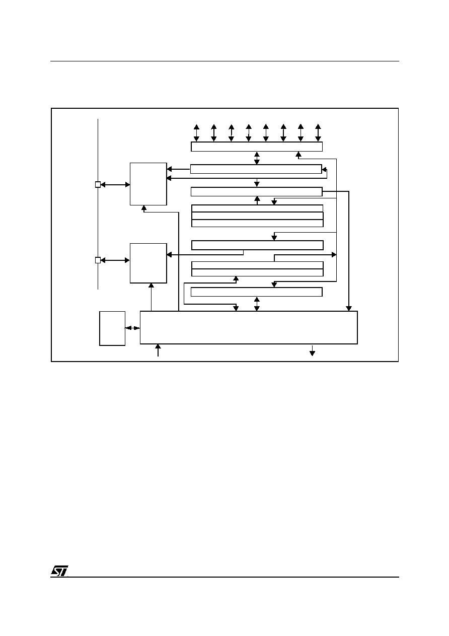
179/230
ST92163 - I2C BUS INTERFACE
I
2
C BUS INTERFACE (Cont'd)
Figure 85. I
2
C Interface Block Diagram
8.5.3 Functional Description
Refer to the I2CCR, I2CSR1 and I2CSR2 registers
in
Section 8.5.7
. for the bit definitions.
The I
2
C interface works as an I/O interface
between the ST9 microcontroller and the I
2
C bus
protocol. In addition to receiving and transmitting
data, the interface converts data from serial to
parallel format and vice versa using an interrupt or
polled handshake.
It operates in Multimaster/slave I
2
C mode. The se-
lection of the operating mode is made by software.
The I
2
C interface is connected to the I
2
C bus by a
data pin (SDA) and a clock pin (SCL) which must
be configured as open drain when the I
2
C cell is
enabled by programming the I/O port bits and the
PE bit in the I2CCR register. In this case, the value
of the external pull-up resistance used depends on
the application.
When the I
2
C cell is disabled, the SDA and SCL
ports revert to being standard I/O port pins.
The I
2
C interface has sixteen internal registers.
Six of them are used for initialization:
≠ Own Address Registers I2COAR1, I2COAR2
≠ General Call Address Register I2CADR
≠ Clock Control Registers I2CCCR, I2CECCR
≠ Control register I2CCR
The following four registers are used during data
transmission/reception:
≠ Data Register I2CDR
≠ Control Register I2CCR
≠ Status Register 1 I2CSR1
≠ Status Register 2 I2CSR2
DATA REGISTER
DATA SHIFT REGISTER
COMPARATOR
OWN ADDRESS REGISTER 2
CLOCK CONTROL REGISTER
STATUS REGISTER 1
CONTROL REGISTER
CONTROL
DATA
CLOCK
CONTROL
LOGIC AND INTERRUPT/DMA REGISTERS
GENERAL CALL ADDRESS
STATUS REGISTER 2
DMA
DATA BUS
CONTROL SIGNALS
INTERRUPT
VR02119A
SDA
SCL
OWN ADDRESS REGISTER 1

180/230
ST92163 - I2C BUS INTERFACE
I
2
C BUS INTERFACE (Cont'd)
The following seven registers are used to handle
the interrupt and the DMA features:
≠ Interrupt Status Register I2CISR
≠ Interrupt Mask Register I2CIMR
≠ Interrupt Vector Register I2CIVR
≠ Receiver DMA Address Pointer Register
I2CRDAP
≠ Receiver DMA Transaction Counter Register
I2CRDC
≠ Transmitter DMA Address Pointer Register
I2CTDAP
≠ Transmitter DMA transaction Counter Register
I2CTDC
The interface can decode both addresses:
≠ Software programmable 7-bit General Call
address
≠ I
2
C address stored by software in the I2COAR1
register in 7-bit address mode or stored in
I2COAR1 and I2COAR2 registers in 10-bit ad-
dress mode.
After a reset, the interface is disabled.
IMPORTANT
:
1. To guarantee correct operation, before enabling
the peripheral (while I2CCR.PE=0), configure bit7
and bit6 of the I2COAR2 register according to the
internal clock INTCLK (for example 11xxxxxxb in
the range 14 - 30 MHz).
2. Bit7 of the I2CCR register must be cleared.
8.5.3.1 Mode Selection
In I
2
C mode, the interface can operate in the four
following modes:
≠ Master transmitter/receiver
≠ Slave transmitter/receiver
By default, it operates in slave mode.
This interface automatically switches from slave to
master after a start condition is generated on the
bus and from master to slave in case of arbitration
loss or stop condition generation.
In Master mode, it initiates a data transfer and
generates the clock signal. A serial data transfer
always begins with a start condition and ends with
a stop condition. Both start and stop conditions are
generated in master mode by software.
In Slave mode, it is able to recognize its own ad-
dress (7 or 10-bit), as stored in the I2COAR1 and
I2COAR2 registers and (when the I2CCR.ENGC
bit is set) the General Call address (stored in
I2CADR register). It never recognizes the Start
Byte (address byte 01h) whatever its own address
is.
Data and addresses are transferred in 8 bits, MSB
first. The first byte(s) following the start condition
contain the address (one byte in 7-bit mode, two
bytes in 10-bit mode). The address is always
transmitted in master mode.
A 9th clock pulse follows the 8 clock cycles of a
byte transfer, during which the receiver must send
an acknowledge bit to the transmitter.
Acknowledge is enabled and disabled by software.
Refer to
Figure 86
.
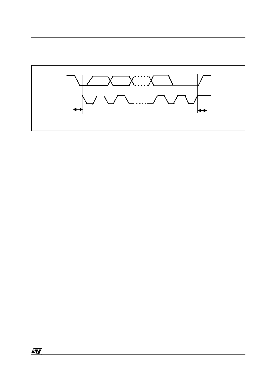
181/230
ST92163 - I2C BUS INTERFACE
I
2
C BUS INTERFACE (Cont'd)
Figure 86. I
2
C BUS Protocol
Any transfer can be done using either the I
2
C
registers directly or via the DMA.
If the transfer is to be done directly by accessing
the I2CDR, the interface waits (by holding the SCL
line low) for software to write in the Data Register
before transmission of a data byte, or to read the
Data Register after a data byte is received.
If the transfer is to be done via DMA, the interface
sends a request for a DMA transfer. Then it waits
for the DMA to complete. The transfer between the
interface and the I
2
C bus will begin on the next
rising edge of the SCL clock.
The SCL frequency (F
scl
) generated in master
mode is controlled by a programmable clock divid-
er. The speed of the I
2
C interface may be selected
between Standard (0-100KHz) and Fast (100-
400KHz) I
2
C modes.
8.5.4 I
2
C State Machine
To enable the interface in I
2
C mode the I2CCR.PE
bit must be set twice as the first write only acti-
vates the interface (only the PE bit is set); and the
bit7 of I2CCR register must be cleared.
The I
2
C interface always operates in slave mode
(the M/SL bit is cleared) except when it initiates a
transmission or a receipt sequencing (master
mode).
The multimaster function is enabled with an auto-
matic switch from master mode to slave mode
when the interface loses the arbitration of the I
2
C
bus.
8.5.4.1 I
2
C Slave Mode
As soon as a start condition is detected, the
address word is received from the SDA line and
sent to the shift register; then it is compared with
the address of the interface or the General Call
address (if selected by software).
Note: In 10-bit addressing mode, the comparison
includes the header sequence (11110xx0) and the
two most significant bits of the address.
s
Header (10-bit mode) or Address (both 10-bit
and 7-bit modes) not matched: the state
machine is reset and waits for another Start
condition.
s
Header matched (10-bit mode only): the
interface generates an acknowledge pulse if the
ACK bit of the control register (I2CCR) is set.
s
Address matched: the I2CSR1.ADSL bit is set
and an acknowledge bit is sent to the master if
the I2CCR.ACK bit is set. An interrupt request
occurs if the I2CCR.ITE bit is set. Then the SCL
line is held low until the microcontroller reads
the I2CSR1 register (see
Figure 87
Transfer
sequencing EV1).
SCL
SDA
1
2
8
9
MSB
ACK
STOP
START
CONDITION
CONDITION
VR02119B

182/230
ST92163 - I2C BUS INTERFACE
I
2
C BUS INTERFACE (Cont'd)
Next, depending on the data direction bit (least
significant bit of the address byte), and after the
generation of an acknowledge, the slave must go
in sending or receiving mode.
In 10-bit mode, after receiving the address se-
quence the slave is always in receive mode. It will
enter transmit mode on receiving a repeated Start
condition followed by the header sequence with
matching address bits and the least significant bit
set (11110xx1).
Slave Receiver
Following the address reception and after I2CSR1
register has been read, the slave receives bytes
from the SDA line into the Shift Register and sends
them to the I2CDR register. After each byte it
generates an acknowledge bit if the I2CCR.ACK
bit is set.
When the acknowledge bit is sent, the
I2CSR1.BTF flag is set and an interrupt is generat-
ed if the I2CCR.ITE bit is set (see
Figure 87
Transfer sequencing EV2).
Then the interface waits for a read of the I2CSR1
register followed by a read of the I2CDR register,
or waits for the DMA to complete.
Slave Transmitter
Following the address reception and after I2CSR1
register has been read, the slave sends bytes from
the I2CDR register to the SDA line via the internal
shift register.
When the acknowledge bit is received, the
I2CCR.BTF flag is set and an interrupt is
generated if the I2CCR.ITE bit is set (see
Figure
87
Transfer sequencing EV3).
The slave waits for a read of the I2CSR1 register
followed by a write in the I2CDR register or waits
for the DMA to complete, both holding the SCL
line low (except on EV3-1).
Error Cases
≠ BERR: Detection of a Stop or a Start condition
during a byte transfer.
The I2CSR2.BERR flag is set and an interrupt is
generated if I2CCR.ITE bit is set.
If it is a stop then the state machine is reset.
If it is a start then the state machine is reset and
it waits for the new slave address on the bus.
≠ AF: Detection of a no-acknowledge bit.
The I2CSR2.AF flag is set and an interrupt is
generated if the I2CCR.ITE bit is set.
Note: In both cases, SCL line is not stretched low;
however, the SDA line, due to possible ´0ª bits
transmitted last, can remain low. It is then neces-
sary to release both lines by software.
Other Events
≠ ADSL: Detection of a Start condition after an ac-
knowledge time-slot.
The state machine is reset and starts a new proc-
ess. The I2CSR1.ADSL flag bit is set and an in-
terrupt is generated if the I2CCR.ITE bit is set.
The SCL line is stretched low.
≠ STOPF: Detection of a Stop condition after an
acknowledge time-slot.
The state machine is reset. Then the
I2CSR2.STOPF flag is set and an interrupt is
generated if the I2CCR.ITE bit is set.
How to release the SDA / SCL lines
Check that the I2CSR1.BUSY bit is reset. Set and
subsequently clear the I2CCR.STOP bit while the
I2CSR1.BTF bit is set; then the SDA/SCL lines are
released immediately after the transfer of the cur-
rent byte.
This will also reset the state machine; any subse-
quent STOP bit (EV4) will not be detected.
8.5.4.2 I
2
C Master Mode
To switch from default Slave mode to Master
mode a Start condition generation is needed.
Setting the I2CCR.START bit while the
I2CSR1.BUSY bit is cleared causes the interface
to generate a Start condition.
Once the Start condition is generated, the periph-
eral is in master mode (I2CSR1.M/SL=1) and
I2CSR1.SB (Start bit) flag is set and an interrupt is
generated if the I2CCR.ITE bit is set (see
Figure
87
Transfer sequencing EV5 event).
The interface waits for a read of the I2CSR1 regis-
ter followed by a write in the I2CDR register with
the Slave address, holding the SCL line low.

183/230
ST92163 - I2C BUS INTERFACE
I
2
C BUS INTERFACE (Cont'd)
Then the slave address is sent to the SDA line.
In 7-bit addressing mode, one address byte is
sent.
In 10-bit addressing mode, sending the first byte
including the header sequence causes the
I2CSR1.EVF and I2CSR1.ADD10 bits to be set by
hardware with interrupt generation if the
I2CCR.ITE bit is set.
Then the master waits for a read of the I2CSR1
register followed by a write in the I2CDR register,
holding the SCL line low (see
Figure 87
Transfer
sequencing EV9). Then the second address byte
is sent by the interface.
After each address byte, an acknowledge clock
pulse is sent to the SCL line if the I2CSR1.EVF
and
≠ I2CSR1.ADD10 bit (if first header)
≠ I2CSR2.ADDTX bit (if address or second head-
er)
are set, and an interrupt is generated if the
I2CCR.ITE bit is set.
The peripheral waits for a read of the I2CSR1 reg-
ister followed by a write into the Control Register
(I2CCR) by holding the SCL line low (see
Figure
87
Transfer sequencing EV6 event).
If there was no acknowledge (I2CSR2.AF=1), the
master must stop or restart the communication
(set the I2CCR.START or I2CCR.STOP bits).
If there was an acknowledge, the state machine
enters a sending or receiving process according to
the data direction bit (least significant bit of the ad-
dress), the I2CSR1.BTF flag is set and an interrupt
is generated if I2CCR.ITE bit is set (see Transfer
sequencing EV7, EV8 events).
If the master loses the arbitration of the bus there
is no acknowledge, the I2CSR2.AF flag is set and
the master must set the START or STOP bit in the
control register (I2CCR).The I2CSR2.ARLO flag is
set, the I2CSR1.M/SL flag is cleared and the proc-
ess is reset. An interrupt is generated if I2CCR.ITE
is set.
Master Transmitter:
The master waits for the microcontroller to write in
the Data Register (I2CDR) or it waits for the DMA
to complete both holding the SCL line low (see
Transfer sequencing EV8).
Then the byte is received into the shift register and
sent to the SDA line. When the acknowledge bit is
received, the I2CSR1.BTF flag is set and an
interrupt is generated if the I2CCR.ITE bit is set or
the DMA is requested.
Note: In 10-bit addressing mode, to switch the
master to Receiver mode, software must generate
a repeated Start condition and resend the header
sequence with the least significant bit set
(11110xx1).
Master Receiver:
The master receives a byte from the SDA line into
the shift register and sends it to the I2CDR regis-
ter. It generates an acknowledge bit if the
I2CCR.ACK bit is set and an interrupt if the
I2CCR.ITE bit is set or a DMA is requested (see
Transfer sequencing EV7 event).
Then it waits for the microcontroller to read the
Data Register (I2CDR) or waits for the DMA to
complete both holding SCL line low.
Error Cases
s
BERR: Detection of a Stop or a Start condition
during a byte transfer.
The I2CSR2.BERR flag is set and an interrupt is
generated if I2CCR.ITE is set.
s
AF: Detection of a no acknowledge bit
The I2CSR2.AF flag is set and an interrupt is
generated if I2CCR.ITE is set.
s
ARLO: Arbitration Lost
The I2CSR2.ARLO flag is set, the I2CSR1.M/SL
flag is cleared and the process is reset. An
interrupt is generated if the I2CCR.ITE bit is set.
Note: In all cases, to resume communications, set
the I2CCR.START or I2CCR.STOP bits.
Events generated by the I
2
C interface
s
STOP condition
When the I2CCR.STOP bit is set, a Stop
condition is generated after the transfer of the
current byte, the I2CSR1.M/SL flag is cleared
and the state machine is reset. No interrupt is
generated in master mode at the detection of
the stop condition.
s
START condition
When the I2CCR.START bit is set, a start
condition is generated as soon as the I
2
C bus is
free. The I2CSR1.SB flag is set and an interrupt
is generated if the I2CCR.ITE bit is set.
184/230
ST92163 - I2C BUS INTERFACE
I
2
C BUS INTERFACE (Cont'd)
Figure 87. Transfer Sequencing
7-bit Slave receiver:
7-bit Slave transmitter:
7-bit Master receiver:
7-bit Master transmitter:
10-bit Slave receiver:
10-bit Slave transmitter:
10-bit Master transmitter
10-bit Master receiver:
Legend:
S=Start, Sr = Repeated Start, P=Stop, A=Acknowledge, NA=Non-acknowledge,
EVx=Event (with interrupt if ITE=1)
EV1: EVF=1, ADSL=1, cleared by reading SR1 register.
EV2: EVF=1, BTF=1, cleared by reading SR1 register followed by reading DR register or when DMA
is complete.
EV3: EVF=1, BTF=1, cleared by reading SR1 register followed by writing DR register or when DMA
is complete.
EV3-1: EVF=1, AF=1, BTF=1; AF is cleared by reading SR1 register, BTF is cleared by releasing the
lines (STOP=1, STOP=0) or writing DR register (for example DR=FFh). Note: If lines are released by
STOP=1, STOP=0 the subsequent EV4 is not seen.
EV4: EVF=1, STOPF=1, cleared by reading SR2 register.
S Address
A
Data1
A
Data2
A
.....
DataN
A
P
EV1
EV2
EV2
EV2
EV4
S Address
A
Data1
A
Data2
A
.....
DataN
NA
P
EV1 EV3
EV3
EV3
EV3-1
EV4
S
Address
A
Data1
A
Data2
A
.....
DataN
NA
P
EV5
EV6
EV7
EV7
EV7
S
Address
A
Data1
A
Data2
A
.....
DataN
A
P
EV5
EV6 EV8
EV8
EV8
EV8
S Header
A
Address
A
Data1
A
.....
DataN
A
P
EV1
EV2
EV2
EV4
S
r
Header
A
Data1
A
....
.
DataN
A
P
EV1 EV3
EV3
EV3-1
EV4
S
Header
A
Address
A
Data1
A
.....
DataN
A
P
EV5
EV9
EV6 EV8
EV8
EV8
S
r
Header
A
Data1
A
.....
DataN
A
P
EV5
EV6
EV7
EV7
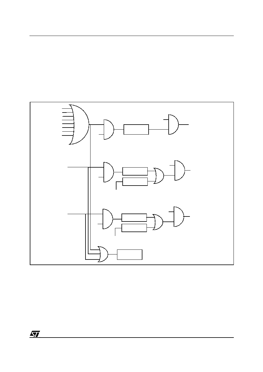
185/230
ST92163 - I2C BUS INTERFACE
EV5: EVF=1, SB=1, cleared by reading SR1 register followed by writing DR register.
EV6: EVF=1, ADDTX=1, cleared by reading SR1 register followed by writing CR register
(for example PE=1).
EV7: EVF=1, BTF=1, cleared by reading SR1 register followed by reading DR register or when DMA
is complete.
EV8: EVF=1, BTF=1, cleared by reading SR1 register followed by writing DR register or when DMA
is complete.
EV9: EVF=1, ADD10=1, cleared by reading SR1 register followed by writing DR register.
Figure 88. Event Flags and Interrupt Generation
ADSL
SB
AF
STOPF
ARLO
BERR
ADD10
ADDTX
ITE
IERRM
IERRP
ERROR
INTERRUPT
REQUEST
BTF=1 & TRA=0
Receiving DMA
ITE
IRXM
IRXP
DATA RECEIVED
INTERRUPT
REQUEST
End Of Block
or
END OF BLOCK
BTF=1 & TRA=1
ITE
READY TO TRANSMIT
INTERRUPT
REQUEST
or
END OF BLOCK
I2CSR1.EVF
REOBP
ITXM
ITXP
TEOBP
Transmitting DMA
End Of Block

186/230
ST92163 - I2C BUS INTERFACE
I
2
C BUS INTERFACE (Cont'd)
8.5.5 Interrupt Features
The I
2
Cbus interface has three interrupt sources
related to "Error Condition", "Peripheral Ready to
Transmit" and "Data Received".
The peripheral uses the ST9+ interrupt internal
protocol without requiring the use of the external
interrupt channel. Dedicated registers of the pe-
ripheral should be loaded with appropriate values
to set the interrupt vector (see the description of
the I2CIVR register), the interrupt mask bits (see
the description of the I2CIMR register) and the in-
terrupt priority and pending bits (see the descrip-
tion of the I2CISR register).
The peripheral also has a global interrupt enable
(the I2CCR.ITE bit) that must be set to enable the
interrupt features. Moreover there is a global inter-
rupt flag (I2CSR1.EVF bit) which is set when one
of the interrupt events occurs (except the End Of
Block interrupts - see the DMA Features section).
The "Data Received" interrupt source occurs after
the acknowledge of a received data byte is per-
formed. It is generated when the I2CSR1.BTF flag
is set and the I2CSR1.TRA flag is zero.
If the DMA feature is enabled in receiver mode,
this interrupt is not generated and the same inter-
rupt vector is used to send a Receiving End Of
Block interrupt (See the DMA feature section).
The "Peripheral Ready To Transmit" interrupt
source occurs as soon as a data byte can be
transmitted by the peripheral. It is generated when
the I2CSR1.BTF and the I2CSR1.TRA flags are
set.
If the DMA feature is enabled in transmitter mode,
this interrupt is not generated and the same inter-
rupt vector is used to send a Transmitting End Of
Block interrupt (See the DMA feature section).
The "Error condition" interrupt source occurs when
one of the following condition occurs:
≠ Address matched in Slave mode while
I2CCR.ACK=1
(I2CSR1.ADSL and I2CSR1.EVF flags = 1)
≠ Start condition generated
(I2CSR1.SB and I2CSR1.EVF flags = 1)
≠ No acknowledge received after byte transmis-
sion
(I2CSR2.AF and I2CSR1.EVF flags = 1)
≠ Stop detected in Slave mode
(I2CSR2.STOPF and I2CSR1.EVF flags = 1)
≠ Arbitration lost in Master mode
(I2CSR2.ARLO and I2CSR1.EVF flags = 1)
≠ Bus error, Start or Stop condition detected
during data transfer
(I2CSR2.BERR and I2CSR1.EVF flags = 1)
≠ Master has sent the header byte
(I2CSR1.ADD10 and I2CSR1.EVF flags = 1)
≠ Address byte successfully transmitted in
Master mode.
(I2CSR1.EVF = 1 and I2CSR2.ADDTX=1)
Note: Depending on the value of I2CISR.DMAS-
TOP bit, the pending bit related to the "error condi-
tion" interrupt source is able to suspend or not sus-
pend DMA transfers.
Each interrupt source has a dedicated interrupt
address pointer vector stored in the I2CIVR regis-
ter. The five more significant bits of the vector ad-
dress are programmable by the customer, where-
as the three less significant bits are set by hard-
ware depending on the interrupt source:
≠ 010: error condition detected
≠ 100: data received
≠ 110: peripheral ready to transmit
The priority with respect to the other peripherals is
programmable by setting the PRL[2:0] bits in the
I2CISR register. The lowest interrupt priority is ob-
tained by setting all the bits (this priority level is
never acknowledged by the CPU and is equivalent
to disabling the interrupts of the peripheral); the
highest interrupt priority is programmed by reset-
ting all the bits. See the Interrupt and DMA chap-
ters for more details.
The internal priority of the interrupt sources of the
peripheral is fixed by hardware with the following
order: "Error Condition" (highest priority), "Data
Received", "Peripheral Ready to Transmit".
Note: The DMA has the highest priority over the
interrupts; moreover the "Transmitting End Of
Block" interrupt has the same priority as the "Pe-
ripheral Ready to Transmit" interrupt and the "Re-
ceiving End Of Block" interrupt has the same prior-
ity as the "Data received" interrupt.
Each of these three interrupt sources has a pend-
ing bit (IERRP, IRXP, ITXP) in the I2CISR register
that is set by hardware when the corresponding in-
terrupt event occurs. An interrupt request is per-
formed only if the corresponding mask bit is set
(IERRM, IRXM, ITXM) in the I2CIMR register and
the peripheral has a proper priority level.
The pending bit has to be reset by software.

187/230
ST92163 - I2C BUS INTERFACE
I
2
C BUS INTERFACE (Cont'd)
Note: Until the pending bit is reset (while the cor-
responding mask bit is set), the peripheral proc-
esses an interrupt request. So, if at the end of an
interrupt routine the pending bit is not reset, anoth-
er interrupt request is performed.
Note: Before the end of the transmission and re-
ception interrupt routines, the I2CSR1.BTF flag bit
should be checked, to acknowledge any interrupt
requests that occurred during the interrupt routine
and to avoid masking subsequent interrupt re-
quests.
Note: The "Error" event interrupt pending bit
(I2CISR.IERRP) is forced high while the error
event flags are set (ADD10, ADSL and SB flags of
the I2CSR1 register; SCLF, ADDTX, AF, STOPF,
ARLO and BERR flags of the I2CSR2 register).
Note: If the I2CISR.DMASTOP bit is reset, then
the DMA has the highest priority with respect to
the interrupts; if the bit is set (as after the MCU re-
set) and the "Error event" pending bit is set
(I2CISR.IERRP), then the DMA is suspended until
the pending bit is reset by software. In the second
case, the "Error" interrupt sources have higher pri-
ority, followed by DMA, "Data received" and "Re-
ceiving End Of Block" interrupts, "Peripheral
Ready to Transmit" and "Transmitting End Of
Block".
Moreover the Transmitting End Of Block interrupt
has the same priority as the "Peripheral Ready to
Transmit" interrupt and the Receiving End Of
Block interrupt has the same priority as the "Data
received" interrupt.
8.5.6 DMA Features
The peripheral can use the ST9+ on-chip Direct
Memory Access (DMA) channels to provide high-
speed data transaction between the peripheral
and contiguous locations of Register File, and
Memory. The transactions can occur from and to-
ward the peripheral. The maximum number of
transactions that each DMA channel can perform
is 222 if the register file is selected or 65536 if
memory is selected. The control of the DMA fea-
tures is performed using registers placed in the pe-
ripheral register page (I2CISR, I2CIMR,
I2CRDAP, I2CRDC, I2CTDAP, I2CTDC).
Each DMA transfer consists of three operations:
≠ A load from/to the peripheral data register
(I2CDR) to/from a location of Register File/Mem-
ory addressed through the DMA Address Regis-
ter (or Register pair)
≠ A post-increment of the DMA Address Register
(or Register pair)
≠ A post-decrement of the DMA transaction coun-
ter, which contains the number of transactions
that have still to be performed.
Depending on the value of the DDCISR.DMAS-
TOP bit the DMA feature can be suspended or not
(both in transmission and in reception) until the
pending bit related to the "Error event" interrupt re-
quest is set.
The priority level of the DMA features of the I
2
C
interface with respect to the other peripherals and
the CPU is the same as programmed in the
I2CISR register for the interrupt sources. In the in-
ternal priority level order of the peripheral, if DD-
CISR.DMASTOP=0, DMA has a higher priority
with respect to the interrupt sources. Otherwise (if
DDCISR.DMASTOP=1), the DMA has a priority
lower than "error" event interrupt sources but
greater than reception and transmission interrupt
sources.
Refer to the Interrupt and DMA chapters for details
on the priority levels.
The DMA features are enabled by setting the cor-
responding enabling bits (RXDM, TXDM) in the
I2CIMR register. It is possible to select also the di-
rection of the DMA transactions.
Once the DMA transfer is completed (the transac-
tion counter reaches 0 value), an interrupt request
to the CPU is generated. This kind of interrupt is
called "End Of Block". The peripheral sends two
different "End Of Block" interrupts depending on
the direction of the DMA (Receiving End Of Block -
Transmitting End Of Block). These interrupt
sources have dedicated interrupt pending bits in
the I2CIMR register (REOBP, TEOBP) and they
are mapped on the same interrupt vectors as re-
spectively "Data Received" and "Peripheral Ready
to Transmit" interrupt sources. The same corre-
spondence exists about the internal priority be-
tween interrupts.
Note: The I2CCR.ITE bit has no effect on the End
Of Block interrupts.
Moreover, the I2CSR1.EVF flag is not set by the
End Of Block interrupts.

188/230
ST92163 - I2C BUS INTERFACE
I
2
C BUS INTERFACE (Cont'd)
8.5.6.1 DMA between Peripheral and Register
File
If the DMA transaction is made between the pe-
ripheral and the Register File, one register is
required to hold the DMA Address and one to hold
the DMA transaction counter.
These two registers must be located in the Regis-
ter File:
≠ the DMA Address Register in the even ad-
dressed register,
≠ the DMA Transaction Counter in the following
register (odd address).
They are pointed to by the DMA Transaction
Counter Pointer Register (I2CRDC register in re-
ceiving, I2CTDC register in transmitting) located in
the peripheral register page.
In order to select the DMA transaction with the
Register File, the control bit I2CRDC.RF/MEM in
receiving mode or I2CTDC.RF/MEM in transmit-
ting mode must be set.
The transaction Counter Register must be initial-
ized with the number of DMA transfers to perform
and will be decremented after each transaction.
The DMA Address Register must be initialized with
the starting address of the DMA table in the Regis-
ter File, and it is increased after each transaction.
These two registers must be located between ad-
dresses 00h and DFh of the Register File.
When the DMA occurs between Peripheral and
Register File, the I2CTDAP register (in transmis-
sion) and the I2CRDAP one (in reception) are not
used.
8.5.6.2 DMA between Peripheral and Memory
Space
If the DMA transaction is made between the pe-
ripheral and Memory, a register pair is required to
hold the DMA Address and another register pair to
hold the DMA Transaction counter. These two
pairs of registers must be located in the Register
File. The DMA Address pair is pointed to by the
DMA Address Pointer Register (I2CRDAP register
in reception, I2CTDAP register in transmission) lo-
cated in the peripheral register page; the DMA
Transaction Counter pair is pointed to by the DMA
Transaction Counter Pointer Register (I2CRDC
register in reception, I2CTDC register in transmis-
sion) located in the peripheral register page.
In order to select the DMA transaction with the
Memory Space, the control bit I2CRDC.RF/MEM
in receiving mode or I2CTDC.RF/MEM in transmit-
ting mode must be reset.
The Transaction Counter registers pair must be in-
itialized with the number of DMA transfers to per-
form and will be decremented after each transac-
tion. The DMA Address register pair must be ini-
tialized with the starting address of the DMA table
in the Memory Space, and it is increased after
each transaction. These two register pairs must be
located between addresses 00h and DFh of the
Register File.
8.5.6.3 DMA in Master Receive
To correctly manage the reception of the last byte
when the DMA in Master Receive mode is used,
the following sequence of operations must be per-
formed:
1. The number of data bytes to be received must
be set to the effective number of bytes minus
one byte.
2. When the Receiving End Of Block condition
occurs, the I2CCR.STOP bit must be set and
the I2CCR.ACK bit must be reset.
The last byte of the reception sequence can be re-
ceived either using interrupts/polling or using
DMA. If the user wants to receive the last byte us-
ing DMA, the number of bytes to be received must
be set to 1, and the DMA in reception must be re-
enabled (IMR.RXDM bit set) to receive the last
byte. Moreover the Receiving End Of Block inter-
rupt service routine must be designed to recognize
and manage the two different End Of Block situa-
tions (after the first sequence of data bytes and af-
ter the last data byte).

189/230
ST92163 - I2C BUS INTERFACE
I
2
C BUS INTERFACE (Cont'd)
8.5.7 Register Description
IMPORTANT
:
1. To guarantee correct operation, before enabling
the peripheral (while I2CCR.PE=0), configure bit7
and bit6 of the I2COAR2 register according to the
internal clock INTCLK (for example 11xxxxxxb in
the range 14 - 30 MHz).
2. Bit7 of the I2CCR register must be cleared.
I
2
C CONTROL REGISTER (I2CCR)
R240 - Read / Write
Register Page: 20
Reset Value: 0000 0000 (00h)
Bit 7:6 = Reserved
Must be cleared
Bit 5 = PE
Peripheral Enable.
This bit is set and cleared by software.
0: Peripheral disabled (reset value)
1: Master/Slave capability
Notes:
≠ When I2CCR.PE=0, all the bits of the I2CCR
register and the I2CSR1-I2CSR2 registers ex-
cept the STOP bit are reset. All outputs will be re-
leased while I2CCR.PE=0
≠ When I2CCR.PE=1, the corresponding I/O pins
are selected by hardware as alternate functions
(open drain).
≠ To enable the I
2
C interface, write the I2CCR reg-
ister TWICE with I2CCR.PE=1 as the first write
only activates the interface (only I2CCR.PE is
set).
≠ When PE=1, the FREQ[2:0] and EN10BIT bits in
the I2COAR2 and I2CADR registers cannot be
written. The value of these bits can be changed
only when PE=0.
Bit 4 = ENGC
General Call address enable.
Setting this bit the peripheral works as a slave and
the value stored in the I2CADR register is recog-
nized as device address.
This bit is set and cleared by software. It is also
cleared by hardware when the interface is disa-
bled (I2CCR.PE=0).
0: The address stored in the I2CADR register is
ignored (reset value)
1: The General Call address stored in the I2CADR
register will be acknowledged
Note: The correct value (usually 00h) must be
written in the I2CADR register before enabling the
General Call feature.
Bit 3 = START
Generation of a Start condition
.
This bit is set and cleared by software. It is also
cleared by hardware when the interface is disa-
bled (I2CCR.PE=0) or when the Start condition is
sent (with interrupt generation if ITE=1).
≠ In master mode:
0: No start generation
1: Repeated start generation
≠ In slave mode:
0: No start generation (reset value)
1: Start generation when the bus is free
Bit 2 = ACK
Acknowledge enable.
This bit is set and cleared by software. It is also
cleared by hardware when the interface is disa-
bled (I2CCR.PE=0).
0: No acknowledge returned (reset value)
1: Acknowledge returned after an address byte or
a data byte is received
Bit 1 = STOP
Generation of a Stop condition
.
This bit is set and cleared by software. It is also
cleared by hardware in master mode. It is not
cleared when the interface is disabled
(I2CCR.PE=0). In slave mode, this bit must be set
only when I2CSR1.BTF=1.
≠ In master mode:
0: No stop generation
1: Stop generation after the current byte transfer
or after the current Start condition is sent. The
STOP bit is cleared by hardware when the Stop
condition is sent.
≠ In slave mode:
0: No stop generation (reset value)
1: Release SCL and SDA lines after the current
byte transfer (I2CSR1.BTF=1). In this mode the
STOP bit has to be cleared by software.
7
0
0
0
PE
ENGC
START ACK STOP ITE

190/230
ST92163 - I2C BUS INTERFACE
I
2
C BUS INTERFACE (Cont'd)
Bit 0 = ITE
Interrupt Enable.
The ITE bit enables the generation of interrupts.
This bit is set and cleared by software and cleared
by hardware when the interface is disabled
(I2CCR.PE=0).
0: Interrupts disabled (reset value)
1: Interrupts enabled after any of the following con-
ditions:
≠ Byte received or to be transmitted
(I2CSR1.BTF and I2CSR1.EVF flags = 1)
≠ Address matched in Slave mode while
I2CCR.ACK=1
(I2CSR1.ADSL and I2CSR1.EVF flags = 1)
≠ Start condition generated
(I2CSR1.SB and I2CSR1.EVF flags = 1)
≠ No acknowledge received after byte transmis-
sion
(I2CSR2.AF and I2CSR1.EVF flags = 1)
≠ Stop detected in Slave mode
(I2CSR2.STOPF and I2CSR1.EVF flags = 1)
≠ Arbitration lost in Master mode
(I2CSR2.ARLO and I2CSR1.EVF flags = 1)
≠ Bus error, Start or Stop condition detected
during data transfer
(I2CSR2.BERR and I2CSR1.EVF flags = 1)
≠ Master has sent header byte
(I2CSR1.ADD10 and I2CSR1.EVF flags = 1)
≠ Address byte successfully transmitted in Mas-
ter mode.
(I2CSR1.EVF = 1 and I2CSR2.ADDTX = 1)
SCL is held low when the ADDTX flag of the
I2CSR2 register or the ADD10, SB, BTF or ADSL
flags of I2CSR1 register are set (See
Figure 87
) or
when the DMA is not complete.
The transfer is suspended in all cases except
when the BTF bit is set and the DMA is enabled. In
this case the event routine must suspend the DMA
transfer if it is required.
I
2
C STATUS REGISTER 1 (I2CSR1)
R241 - Read Only
Register Page: 20
Reset Value: 0000 0000 (00h)
Note: Some bits of this register are reset by a read
operation of the register. Care must be taken when
using instructions that work on single bit. Some of
them perform a read of all the bits of the register
before modifying or testing the wanted bit. So oth-
er bits of the register could be affected by the op-
eration.
In the same way, the test/compare operations per-
form a read operation.
Moreover, if some interrupt events occur while the
register is read, the corresponding flags are set,
and correctly read, but if the read operation resets
the flags, no interrupt request occurs.
Bit 7 = EVF
Event Flag.
This bit is set by hardware as soon as an event (
listed below or described in
Figure 87
) occurs. It is
cleared by software when all event conditions that
set the flag are cleared. It is also cleared by hard-
ware when the interface is disabled
(I2CCR.PE=0).
0: No event
1: One of the following events has occurred:
≠ Byte received or to be transmitted
(I2CSR1.BTF and I2CSR1.EVF flags = 1)
≠ Address matched in Slave mode while
I2CCR.ACK=1
(I2CSR1.ADSL and I2CSR1.EVF flags = 1)
≠ Start condition generated
(I2CSR1.SB and I2CSR1.EVF flags = 1)
≠ No acknowledge received after byte transmis-
sion
(I2CSR2.AF and I2CSR1.EVF flags = 1)
≠ Stop detected in Slave mode
(I2CSR2.STOPF and I2CSR1.EVF flags = 1)
≠ Arbitration lost in Master mode
(I2CSR2.ARLO and I2CSR1.EVF flags = 1)
≠ Bus error, Start or Stop condition detected
during data transfer
(I2CSR2.BERR and I2CSR1.EVF flags = 1)
≠ Master has sent header byte
(I2CSR1.ADD10 and I2CSR1.EVF flags = 1)
7
0
EVF
ADD10
TRA
BUSY
BTF
ADSL
M/SL
SB

191/230
ST92163 - I2C BUS INTERFACE
I
2
C BUS INTERFACE (Cont'd)
≠ Address byte successfully transmitted in Mas-
ter mode.
(I2CSR1.EVF = 1 and I2CSR2.ADDTX=1)
Bit 6 = ADD10
10-bit addressing in Master mode.
This bit is set when the master has sent the first
byte in 10-bit address mode. An interrupt is gener-
ated if ITE=1.
It is cleared by software reading I2CSR1 register
followed by a write in the I2CDR register of the
second address byte. It is also cleared by hard-
ware when peripheral is disabled (I2CCR.PE=0)
or when the STOPF bit is set.
0: No ADD10 event occurred.
1: Master has sent first address byte (header).
Bit 5 = TRA
Transmitter/ Receiver.
When BTF flag of this register is set and also
TRA=1, then a data byte has to be transmitted. It is
cleared automatically when BTF is cleared. It is
also cleared by hardware after the STOPF flag of
I2CSR2 register is set, loss of bus arbitration
(ARLO flag of I2CSR2 register is set) or when the
interface is disabled (I2CCR.PE=0).
0: A data byte is received (if I2CSR1.BTF=1)
1: A data byte can be transmitted (if
I2CSR1.BTF=1)
Bit 4 = BUSY
Bus Busy
.
It indicates a communication in progress on the
bus. The detection of the communications is al-
ways active (even if the peripheral is disabled).
This bit is set by hardware on detection of a Start
condition and cleared by hardware on detection of
a Stop condition. This information is still updated
when the interface is disabled (I2CCR.PE=0).
0: No communication on the bus
1: Communication ongoing on the bus
Bit 3 = BTF
Byte Transfer Finished.
This bit is set by hardware as soon as a byte is cor-
rectly received or before the transmission of a data
byte with interrupt generation if ITE=1. It is cleared
by software reading I2CSR1 register followed by a
read or write of I2CDR register or when DMA is
complete. It is also cleared by hardware when the
interface is disabled (I2CCR.PE=0).
≠ Following a byte transmission, this bit is set after
reception of the acknowledge clock pulse. BTF is
cleared by reading I2CSR1 register followed by
writing the next byte in I2CDR register or when
DMA is complete.
≠ Following a byte reception, this bit is set after
transmission of the acknowledge clock pulse if
ACK=1. BTF is cleared by reading I2CSR1 reg-
ister followed by reading the byte from I2CDR
register or when DMA is complete.
The SCL line is held low while I2CSR1.BTF=1.
0: Byte transfer not done
1: Byte transfer succeeded
Bit 2 = ADSL
Address matched (Slave mode).
This bit is set by hardware if the received slave ad-
dress matches the I2COAR1/I2COAR2 register
content or a General Call address. An interrupt is
generated if ITE=1. It is cleared by software
reading I2CSR1 register or by hardware when the
interface is disabled (I2CCR.PE=0). The SCL line
is held low while ADSL=1.
0: Address mismatched or not received
1: Received address matched
Bit 1 = M/SL
Master/Slave.
This bit is set by hardware as soon as the interface
is in Master mode (Start condition generated on
the lines after the I2CCR.START bit is set). It is
cleared by hardware after detecting a Stop condi-
tion on the bus or a loss of arbitration (ARLO=1). It
is also cleared when the interface is disabled
(I2CCR.PE=0).
0: Slave mode
1: Master mode
Bit 0 = SB
Start Bit (Master mode).
This bit is set by hardware as soon as the Start
condition is generated (following a write of
START=1 if the bus is free). An interrupt is gener-
ated if ITE=1. It is cleared by software reading
I2CSR1 register followed by writing the address
byte in I2CDR register. It is also cleared by hard-
ware when the interface is disabled
(I2CCR.PE=0).
The SCL line is held low while SB=1.
0: No Start condition
1: Start condition generated

192/230
ST92163 - I2C BUS INTERFACE
I
2
C BUS INTERFACE (Cont'd)
I
2
C STATUS REGISTER 2 (I2CSR2)
R242 - Read Only
Register Page: 20
Reset Value: 0000 0000 (00h)
Note: Some bits of this register are reset by a read
operation of the register. Care must be taken when
using instructions that work on single bit. Some of
them perform a read of all the bits of the register
before modifying or testing the wanted bit. So oth-
er bits of the register could be affected by the op-
eration.
In the same way, the test/compare operations per-
form a read operation.
Moreover, if some interrupt events occur while the
register is read, the corresponding flags are set,
and correctly read, but if the read operation resets
the flags, no interrupt request occurs.
Bits 7:6 = Reserved. Forced to 0 by hardware.
Bit 5 = ADDTX
Address or 2nd header transmitted
in Master mode.
This bit is set by hardware when the peripheral,
enabled in Master mode, has received the ac-
knowledge relative to:
≠ Address byte in 7-bit mode
≠ Address or 2nd header byte in 10-bit mode.
0: No address or 2nd header byte transmitted
1: Address or 2nd header byte transmitted.
Bit 4 = AF
Acknowledge Failure
.
This bit is set by hardware when no acknowledge
is returned. An interrupt is generated if ITE=1.
It is cleared by software reading I2CSR2 register
after the falling edge of the acknowledge SCL
pulse, or by hardware when the interface is disa-
bled (I2CCR.PE=0).
The SCL line is not held low while AF=1.
0: No acknowledge failure detected
1: A data or address byte was not acknowledged
Bit 3 = STOPF
Stop Detection (Slave mode).
This bit is set by hardware when a Stop condition
is detected on the bus after an acknowledge. An
interrupt is generated if ITE=1.
It is cleared by software reading I2CSR2 register
or by hardware when the interface is disabled
(I2CCR.PE=0).
The SCL line is not held low while STOPF=1.
0: No Stop condition detected
1: Stop condition detected (while slave receiver)
Bit 2 = ARLO
Arbitration Lost
.
This bit is set by hardware when the interface (in
master mode) loses the arbitration of the bus to
another master. An interrupt is generated if ITE=1.
It is cleared by software reading I2CSR2 register
or by hardware when the interface is disabled
(I2CCR.PE=0).
After an ARLO event the interface switches back
automatically to Slave mode (M/SL=0).
The SCL line is not held low while ARLO=1.
0: No arbitration lost detected
1: Arbitration lost detected
Bit 1 = BERR
Bus Error.
This bit is set by hardware when the interface de-
tects a Start or Stop condition during a byte trans-
fer. An interrupt is generated if ITE=1.
It is cleared by software reading I2CSR2 register
or by hardware when the interface is disabled
(I2CCR.PE=0).
The SCL line is not held low while BERR=1.
Note: If a misplaced start condition is detected,
also the ARLO flag is set; moreover, if a misplaced
stop condition is placed on the acknowledge SCL
pulse, also the AF flag is set.
0: No Start or Stop condition detected during byte
transfer
1: Start or Stop condition detected during byte
transfer
Bit 0 = GCAL
General Call address matched.
This bit is set by hardware after an address
matches with the value stored in the I2CADR reg-
ister while ENGC=1. In the I2CADR the General
Call address must be placed before enabling the
peripheral.
It is cleared by hardware after the detection of a
Stop condition, or when the peripheral is disabled
(I2CCR.PE=0).
0: No match
1: General Call address matched.
7
0
0
0
ADDTX
AF
STOPF ARLO
BERR
GCAL

193/230
ST92163 - I2C BUS INTERFACE
I
2
C BUS INTERFACE (Cont'd)
I
2
C CLOCK CONTROL REGISTER
(I2CCCR)
R243 - Read / Write
Register Page: 20
Reset Value: 0000 0000 (00h)
Bit 7 = FM/SM
Fast/Standard I
2
C mode.
This bit is used to select between fast and stand-
ard mode. See the description of the following bits.
It is set and cleared by software. It is not cleared
when the peripheral is disabled (I2CCR.PE=0)
Bits 6:0 = CC[6:0]
9-bit divider programming
Implementation of a programmable clock divider.
These bits and the CC[8:7] bits of the I2CECCR
register select the speed of the bus (F
SCL
) de-
pending on the I
2
C mode.
They are not cleared when the interface is disa-
bled (I2CCR.PE=0).
≠ Standard mode (FM/SM=0): F
SCL
<= 100kHz
F
SCL
= INTCLK/(2x([CC8..CC0]+2))
≠ Fast mode (FM/SM=1): F
SCL
> 100kHz
F
SCL
= INTCLK/(3x([CC8..CC0]+2))
Note: The programmed frequency is available
with no load on SCL and SDA pins.
I
2
C OWN ADDRESS REGISTER 1
(I2COAR1)
R244 - Read / Write
Register Page:20
Reset Value: 0000 0000 (00h)
7-bit Addressing Mode
Bits 7:1 = ADD[7:1]
Interface address
.
These bits define the I
2
C bus address of the inter-
face.
They are not cleared when the interface is disa-
bled (I2CCR.PE=0).
Bit 0 = ADD0
Address direction bit.
This bit is don't care; the interface acknowledges
either 0 or 1.
It is not cleared when the interface is disabled
(I2CCR.PE=0).
Note: Address 01h is always ignored.
10-bit Addressing Mode
Bits 7:0 = ADD[7:0]
Interface address
.
These are the least significant bits of the I
2
Cbus
address of the interface.
They are not cleared when the interface is disa-
bled (I2CCR.PE=0).
7
0
FM/SM
CC6
CC5
CC4
CC3
CC2 CC1 CC0
7
0
ADD7 ADD6 ADD5 ADD4 ADD3 ADD2 ADD1 ADD0
194/230
ST92163 - I2C BUS INTERFACE
I
2
C BUS INTERFACE (Cont'd)
I
2
C OWN ADDRESS REGISTER 2 (I2COAR2)
R245 - Read / Write
Register Page: 20
Reset Value: 0000 0000 (00h)
Bits 7:6,4 = FREQ[2:0]
Frequency bits.
IMPORTANT: To guarantee correct operation,
set these bits before enabling the interface
(while I2CCR.PE=0).
These bits can be set only when the interface is
disabled (I2CCR.PE=0). To configure the interface
to I
2
C specified delays, select the value corre-
sponding to the microcontroller internal frequency
INTCLK.
Note: If an incorrect value, with respect to the
MCU internal frequency, is written in these bits,
the timings of the peripheral will not meet the I
2
C
bus standard requirements.
Note: The FREQ[2:0] = 101, 110, 111 configura-
tions must not be used.
Bit 5 = EN10BIT
Enable 10-bit I
2
Cbus mode
.
When this bit is set, the 10-bit I
2
Cbus mode is en-
abled.
This bit can be written only when the peripheral is
disabled (I2CCR.PE=0).
0: 7-bit mode selected
1: 10-bit mode selected
Bits 4:3 = Reserved.
Bits 2:1 = ADD[9:8]
Interface address
.
These are the most significant bits of the I
2
Cbus
address of the interface (10-bit mode only). They
are not cleared when the interface is disabled
(I2CCR.PE=0).
Bit 0 = Reserved.
I
2
C DATA REGISTER (I2CDR)
R246 - Read / Write
Register Page: 20
Reset Value: 0000 0000 (00h)
Bits 7:0 = DR[7:0]
I2C Data.
≠ In transmitter mode:
I2CDR contains the next byte of data to be trans-
mitted. The byte transmission begins after the
microcontroller has written in I2CDR or on the
next rising edge of the clock if DMA is complete.
≠ In receiver mode:
I2CDR contains the last byte of data received.
The next byte receipt begins after the I2CDR
read by the microcontroller or on the next rising
edge of the clock if DMA is complete.
GENERAL CALL ADDRESS (I2CADR)
R247 - Read / Write
Register Page: 20
Reset Value: 1010 0000 (A0h)
Bits 7:0 = ADR[7:0]
Interface address
.
These bits define the I
2
Cbus General Call address
of the interface. It must be written with the correct
value depending on the use of the peripheral.If the
peripheral is used in I
2
C bus mode, the 00h value
must be loaded as General Call address.
The customer could load the register with other
values.
The bits can be written only when the peripheral is
disabled (I2CCR.PE=0)
The ADR0 bit is don't care; the interface acknowl-
edges either 0 or 1.
Note: Address 01h is always ignored.
7
0
FREQ1 FREQ0 EN10BIT FREQ2
0
ADD9
ADD8
0
INTCLK
Range
(MHz)
FREQ2
FREQ1
FREQ0
2.5 - 6
0
0
0
6- 10
0
0
1
10- 14
0
1
0
14 - 30
0
1
1
30 - 50
1
0
0
7
0
DR7
DR6
DR5
DR4
DR3
DR2
DR1
DR0
7
0
ADR7 ADR6 ADR5 ADR4 ADR3 ADR2 ADR1 ADR0

195/230
ST92163 - I2C BUS INTERFACE
I
2
C BUS INTERFACE (Cont'd)
INTERRUPT STATUS REGISTER (I2CISR)
R248 - Read / Write
Register Page: 20
Reset Value: 1xxx xxxx (xxh)
Bit 7 = DMASTOP
DMA suspended mode
.
This bit selects between DMA suspended mode
and DMA not suspended mode.
In DMA Suspended mode, if the error interrupt
pending bit (I2CISR.IERRP) is set, no DMA re-
quest is performed. DMA requests are performed
only when IERRP=0. Moreover the "Error Condi-
tion" interrupt source has a higher priority than the
DMA.
In DMA Not-Suspended mode, the status of
IERRP bit has no effect on DMA requests. Moreo-
ver the DMA has higher priority with respect to oth-
er interrupt sources.
0: DMA Suspended mode
1: DMA Not-Suspended mode
Bits 6:4 = PRL[2:0]
Interrupt/DMA Priority Bits
.
The priority is encoded with these three bits. The
value of "0" has the highest priority, the value "7"
has no priority. After the setting of this priority lev-
el, the priorities between the different Interrupt/
DMA sources is hardware defined according with
the following scheme:
≠ Error condition Interrupt (If DMASTOP=1) (High-
est priority)
≠ Receiver DMA request
≠ Transmitter DMA request
≠ Error Condition Interrupt (If DMASTOP=0
≠ Data Received/Receiver End Of Block
≠ Peripheral Ready To Transmit/Transmitter End
Of Block (Lowest priority)
Bit 3 = Reserved.
Must be cleared.
Bit 2 = IERRP
Error Condition pending bit
0: No error
1: Error event detected (if ITE=1)
Note: Depending on the status of the
I2CISR.DMASTOP bit, this flag can suspend or
not suspend the DMA requests.
Note: The Interrupt pending bits can be reset by
writing a "0" but is not possible to write a "1". It is
mandatory to clear the interrupt source by writing a
"0" in the pending bit when executing the interrupt
service routine. When serving an interrupt routine,
the user should reset ONLY the pending bit related
to the served interrupt routine (and not reset the
other pending bits).
To detect the specific error condition that oc-
curred, the flag bits of the I2CSR1 and I2CSR2
register should be checked.
Note: The IERRP pending bit is forced high while
the error event flags are set (ADSL and SB flags in
the I2CSR1 register, SCLF, ADDTX, AF, STOPF,
ARLO and BERR flags in the I2CSR2 register). If
at least one flag is set, it is not possible to reset the
IERRP bit.
Bit 1 = IRXP
Data Received pending bit
0: No data received
1: data received (if ITE=1).
Bit 0 = ITXP
Peripheral Ready To Transmit pend-
ing bit
0: Peripheral not ready to transmit
1: Peripheral ready to transmit a data byte (if
ITE=1).
7
0
DMASTOP PRL2 PRL1 PRL0
0
IERRP IRXP ITXP
196/230
ST92163 - I2C BUS INTERFACE
I
2
C BUS INTERFACE (Cont'd)
INTERRUPT VECTOR REGISTER (I2CIVR)
R249 - Read / Write
Register Page: 20
Reset Value: Undefined
Bits 7:3 = V[7:3]
Interrupt Vector Base Address
.
User programmable interrupt vector bits. These
are the five more significant bits of the interrupt
vector base address. They must be set before en-
abling the interrupt features.
Bits 2:1 = EV[2:1]
Encoded Interrupt Source
.
These Read-Only bits are set by hardware accord-
ing to the interrupt source:
≠ 01: error condition detected
≠ 10: data received
≠ 11: peripheral ready to transmit
Bit 0 = Reserved.
Forced by hardware to 0.
RECEIVER DMA SOURCE ADDRESS POINTER
REGISTER (I2CRDAP)
R250 - Read / Write
Register Page: 20
Reset Value: Undefined
Bits 7:1 = RA[7:1]
Receiver DMA Address Pointer
.
I2CRDAP contains the address of the pointer (in
the Register File) of the Receiver DMA data
source when the DMA is selected between the
peripheral and the Memory Space. Otherwise,
(DMA between peripheral and Register file), this
register has no meaning.
See
Section 8.5.6.1
for more details on the use of
this register.
Bit 0 = RPS
Receiver DMA Memory Pointer Selec-
tor
.
If memory has been selected for DMA transfer
(DDCRDC.RF/MEM = 0) then:
0: Select ISR register for Receiver DMA transfer
address extension.
1: Select DMASR register for Receiver DMA trans-
fer address extension.
RECEIVER DMA TRANSACTION COUNTER
REGISTER (I2CRDC)
R251 - Read / Write
Register Page: 20
Reset Value: Undefined
Bits 7:1 = RC[7:1]
Receiver DMA Counter Pointer.
I2CRDC contains the address of the pointer (in the
Register File) of the DMA receiver transaction
counter when the DMA between Peripheral and
Memory Space is selected. Otherwise (DMA be-
tween Peripheral and Register File), this register
points to a pair of registers that are used as DMA
Address register and DMA Transaction Counter.
See
Section 8.5.6.1
and
Section 8.5.6.2
for more
details on the use of this register.
Bit 0 = RF/MEM
Receiver Register File/ Memory
Selector.
0: DMA towards Memory
1: DMA towards Register file
7
0
V7
V6
V5
V4
V3
EV2
EV1
0
7
0
RA7 RA6 RA5
RA4 RA3 RA2
RA1
RPS
7
0
RC7 RC6 RC5 RC4 RC3 RC2 RC1 RF/MEM

197/230
ST92163 - I2C BUS INTERFACE
I
2
C BUS INTERFACE (Cont'd)
TRANSMITTER DMA SOURCE ADDRESS
POINTER REGISTER (I2CTDAP)
R252 - Read / Write
Register Page: 20
Reset Value: Undefined
Bits 7:1= TA[7:1]
Transmit DMA Address Pointer.
I2CTDAP contains the address of the pointer (in
the Register File) of the Transmitter DMA data
source when the DMA between the peripheral and
the Memory Space is selected. Otherwise (DMA
between the peripheral and Register file), this reg-
ister has no meaning.
See
Section 8.5.6.2
for more details on the use of
this register.
Bit 0 = TPS
Transmitter DMA Memory Pointer Se-
lector
.
If memory has been selected for DMA transfer
(DDCTDC.RF/MEM = 0) then:
0: Select ISR register for transmitter DMA transfer
address extension.
1: Select DMASR register for transmitter DMA
transfer address extension.
TRANSMITTER DMA TRANSACTION COUN-
TER REGISTER (I2CTDC)
R253 - Read / Write
Register Page: 20
Reset Value: Undefined
Bits 7:1 = TC[7:1]
Transmit DMA Counter Pointer
.
I2CTDC contains the address of the pointer (in the
Register File) of the DMA transmitter transaction
counter when the DMA between Peripheral and
Memory Space is selected. Otherwise, if the DMA
between Peripheral and Register File is selected,
this register points to a pair of registers that are
used as DMA Address register and DMA Transac-
tion Counter.
See
Section 8.5.6.1
and
Section 8.5.6.2
for more
details on the use of this register.
Bit 0 = RF/MEM
Transmitter Register File/ Memo-
ry Selector.
0: DMA from Memory
1: DMA from Register file
EXTENDED CLOCK CONTROL REGISTER
(I2CECCR)
R254 - Read / Write
Register Page: 20
Reset Value: 0000 0000 (00h)
Bits 7:2 = Reserved. Must always be cleared.
Bits 1:0 = CC[8:7]
9-bit divider programming
Implementation of a programmable clock divider.
These bits and the CC[6:0] bits of the I2CCCR reg-
ister select the speed of the bus (F
SCL
).
For a description of the use of these bits, see the
I2CCCR register.
They are not cleared when the interface is disa-
bled (I2CCCR.PE=0).
7
0
TA7
TA6
TA5
TA4
TA3
TA2
TA1
TPS
7
0
TC7
TC6
TC5
TC4
TC3
TC2
TC1 RF/MEM
7
0
0
0
0
0
0
0
CC8 CC7

198/230
ST92163 - I2C BUS INTERFACE
I
2
C BUS INTERFACE (Cont'd)
INTERRUPT MASK REGISTER (I2CIMR)
R255 - Read / Write
Register Page: 20
Reset Value: 00xx 0000 (x0h)
Bit 7 = RXDM
Receiver DMA Mask
.
0: DMA reception disable.
1: DMA reception enable
RXDM is reset by hardware when the transaction
counter value decrements to zero, that is when a
Receiver End Of Block interrupt is issued.
Bit 6 = TXDM
Transmitter DMA Mask
.
0: DMA transmission disable.
1: DMA transmission enable.
TXDM is reset by hardware when the transaction
counter value decrements to zero, that is when a
Transmitter End Of Block interrupt is issued.
Bit 5 = REOBP
Receiver DMA End Of Block Flag
.
REOBP should be reset by software in order to
avoid undesired interrupt routines, especially in in-
itialization routine (after reset) and after entering
the End Of Block interrupt routine.Writing "0" in
this bit will cancel the interrupt request
Note: REOBP can only be written to "0".
0: End of block not reached.
1: End of data block in DMA receiver detected
Bit 4 = TEOBP
Transmitter DMA End Of Block
TE-
OBP should be reset by software in order to avoid
undesired interrupt routines, especially in initializa-
tion routine (after reset) and after entering the End
Of Block interrupt routine.Writing "0" will cancel the
interrupt request.
Note: TEOBP can only be written to "0".
0: End of block not reached
1: End of data block in DMA transmitter detected.
Bit 3 = Reserved. This bit must be cleared.
Bit 2 = IERRM
Error Condition interrupt mask bit.
This bit enables/ disables the Error interrupt.
0: Error interrupt disabled.
1: Error Interrupt enabled.
Bit 1 = IRXM
Data Received interrupt mask bit.
This bit enables/ disables the Data Received and
Receive DMA End of Block interrupts.
0: Interrupts disabled
1: Interrupts enabled
Note: This bit has no effect on DMA transfer
Bit 0 = ITXM
Peripheral Ready To Transmit inter-
rupt mask bit.
This bit enables/ disables the Peripheral Ready To
Transmit and Transmit DMA End of Block inter-
rupts.
0: Interrupts disabled
1: Interrupts enabled
Note: This bit has no effect on DMA transfer.
7
0
RXD
M
TXD
M
REOBP TEOBP
0
IERR
M
IRX
M
ITX
M

199/230
ST92163 - I2C BUS INTERFACE
I
2
C BUS INTERFACE (Cont'd)
Table 38. I
2
C BUS Register Map and Reset Values
Address
(Hex.)
Register
Name
7
6
5
4
3
2
1
0
F0h
I2CCR
Reset Value
-
0
-
0
PE
0
ENGC
0
START
0
ACK
0
STOP
0
ITE
0
F1h
I2CSR1
Reset Value
EVF
0
ADD10
0
TRA
0
BUSY
0
BTF
0
ADSL
0
M/SL
0
SB
0
F2h
I2CSR2
Reset Value
-
0
0
0
ADDTX
0
AF
0
STOPF
0
ARLO
0
BERR
0
GCAL
0
F3h
I2CCCR
Reset Value
FM/SM
0
CC6
0
CC5
0
CC4
0
CC3
0
CC2
0
CC1
0
CC0
0
F4h
I2COAR1
Reset Value
ADD7
0
ADD6
0
ADD5
0
ADD4
0
ADD3
0
ADD2
0
ADD1
0
ADD0
0
F5h
I2COAR2
Reset Value
FREQ1
0
FREQ0
0
EN10BIT
0
FREQ2
0
0
0
ADD9
0
ADD8
0
0
0
F6h
I2CDR
Reset Value
DR7
0
DR6
0
DR5
0
DR4
0
DR3
0
DR2
0
DR1
0
DR0
0
F7h
I2CADR
Reset Value
ADR7
1
ADR6
0
ADR5
1
ADR4
0
ADR3
0
ADR2
0
ADR1
0
ADR0
0
F8h
I2CISR
Reset Value
DMASTOP
1
PRL2
X
PRL1
X
PRL0
X
X
IERRP
X
IRXP
X
ITXP
X
F9h
I2CIVR
Reset Value
V7
X
V6
X
V5
X
V4
X
V3
X
EV2
X
EV1
X
0
0
FAh
I2CRDAP
Reset Value
RA7
X
RA6
X
RA5
X
RA4
X
RA3
X
RA2
X
RA1
X
RPS
X
FBh
I2CRDC
Reset Value
RC7
X
RC6
X
RC5
X
RC4
X
RC3
X
RC2
X
RC1
X
RF/MEM
X
FCh
I2CTDAP
Reset Value
TA7
X
TA6
X
TA5
X
TA4
X
TA3
X
TA2
X
TA1
X
TPS
X
FDh
I2CTDC
Reset Value
TC7
X
TC6
X
TC5
X
TC4
X
TC3
X
TC2
X
TC1
X
RF/MEM
X
FEh
I2CECCR
0
0
0
0
0
0
0
0
0
0
0
0
CC8
0
CC7
0
FFh
I2CIMR
Reset Value
RXDM
0
TXDM
0
REOBP
X
TEOBP
X
0
IERRM
0
IRXM
0
ITXM
0
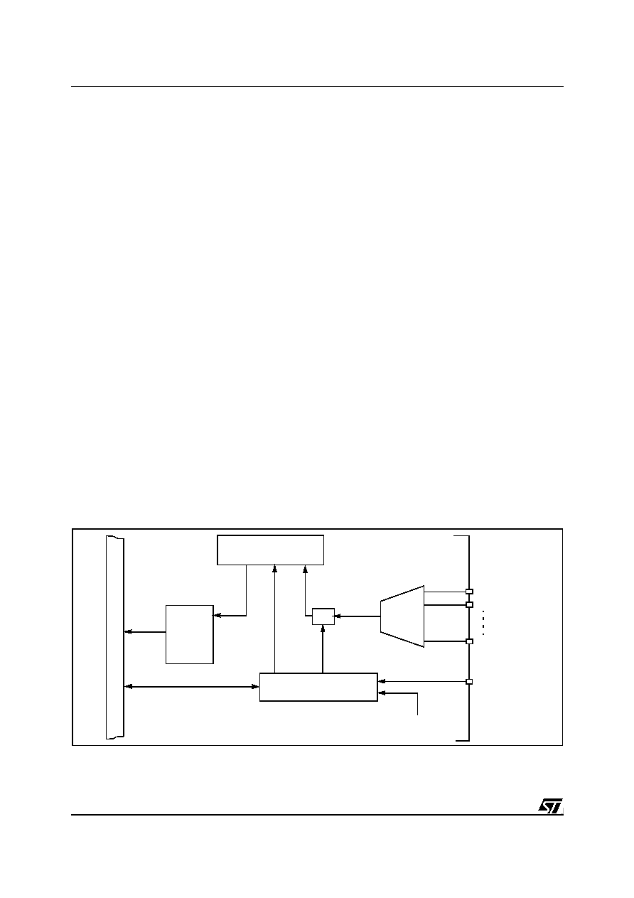
200/230
ST92163 - A/D CONVERTER (A/D)
8.6 A/D CONVERTER (A/D)
8.6.1 Introduction
The 8 bit Analog to Digital Converter uses a fully
differential analog configuration for the best noise
immunity and precision performance. The analog
voltage references of the converter are connected
to the internal AV
DD
& AV
SS
analog supply pins of
the chip if they are available, otherwise to the ordi-
nary V
DD
and V
SS
supply pins of the chip. The
guaranteed accuracy depends on the device (see
Electrical Characteristics). A fast Sample/Hold al-
lows quick signal sampling for minimum warping
effect and conversion error.
8.6.2 Main Features
s
8-bit resolution A/D Converter
s
Single Conversion Time (including Sampling
Time):
≠ 138 internal system clock periods in slow
mode (~5.6 µs @25Mhz internal system
clock);
≠ 78 INTCLK periods in fast mode (~6.5 µs @
12MHZ internal system clock)
s
Sample/Hold: Tsample=
≠ 84 INTCLK periods in slow mode (~3.4 µs
@25Mhz internal system clock)
≠ 48 INTCLK periods in fast mode (~4 µs
@12Mhz internal system clock)
s
Up to 8 Analog Inputs (the number of inputs is
device dependent, see device pinout)
s
Single/Continuous Conversion Mode
s
External/Internal source Trigger (Alternate
synchronization)
s
Power Down mode (Zero Power Consumption)
s
1 Control Logic Register
s
1 Data Register
8.6.3 General Description
Depending on the device, up to 8 analog inputs
can be selected by software.
Different conversion modes are provided: single,
continuous, or triggered. The continuous mode
performs a continuous conversion flow of the se-
lected channel, while in the single mode the se-
lected channel is converted once and then the log-
ic waits for a new hardware or software restart.
A data register (ADDTR) is available, mapped in
page 62, allowing data storage (in single or contin-
uous mode).
The start conversion event can be managed by
software, writing the START/STOP bit of the Con-
trol Logic Register or by hardware using either:
≠ An external signal on the EXTRG triggered input
(negative edge sensitive) connected as an Alter-
nate Function to an I/O port bit
≠ An On Chip Event generated by another periph-
eral, such as the MFT (Multifunction Timer).
Figure 89. A/D Converter Block Diagram
n
ST
9
BU
S
SUCCESSIVE
APPROXIMATION
REGISTER
ANALOG
MUX
DATA
REGISTER
CONTROL LOGIC
S/H
Ain1
Ainx
INTRG
(On Chip Event)
Ain0
EXTRG
201/230
ST92163 - A/D CONVERTER (A/D)
A/D CONVERTER (Cont'd)
The conversion technique used is successive ap-
proximation, with AC coupled analog fully differen-
tial comparators blocks plus a Sample and Hold
logic and a reference generator.
The internal reference (DAC) is based on the use
of a binary-ratioed capacitor array. This technique
allows the specified monotonicity (using the same
ratioed capacitors as sampling capacitor). A Pow-
er Down programmable bit sets the A/D converter
analog section to a zero consumption idle status.
8.6.3.1 Operating Modes
The two main operating modes, single and contin-
uous, can be selected by writing 0 (reset value) or
1 into the CONT bit of the Control Logic Register.
Single Mode
In single mode (CONT=0 in ADCLR) the STR bit is
forced to '0' after the end of channel i-th conver-
sion; then the A/D waits for a new start event. This
mode is useful when a set of signals must be sam-
pled at a fixed frequency imposed by a Timer unit
or an external generator (through the alternate
synchronization feature). A simple software rou-
tine monitoring the STR bit can be used to save
the current value before a new conversion ends
(so to create a signal samples table within the in-
ternal memory or the Register File). Furthermore,
if the R242.0 bit (register AD-INT, bit 0) is set, at
the end of conversion a negative edge on the con-
nected external interrupt channel (see Interrupts
Chapter) is generated to allow the reading of the
converted data by means of an interrupt routine.
Continuous Mode
In continuous mode (CONT=1 in ADCLR) a con-
tinuous conversion flow is entered by a start event
on the selected channel until the STR bit is reset
by software.
At the end of each conversion, the Data Register
(ADCDR) content is updated with the last conver-
sion result, while the former value is lost. When the
conversion flow is stopped, an interrupt request is
generated with the same modality previously de-
scribed.
8.6.3.2 Alternate Synchronization
This feature is available in both single/continuous
modes. The negative edge of external EXTRG sig-
nal or the occurrence of an on-chip event generat-
ed by another peripheral can be used to synchro-
nize the conversion start with a trigger pulse.
These events can be enabled or masked by pro-
gramming the TRG bit in the ADCLR Register.
The effect of alternate synchronization is to set the
STR bit, which is cleared by hardware at the end of
each conversion in single mode. In continuous
mode any trigger pulse following the first one will
be ignored. The synchronization source must pro-
vide a pulse (1.5 internal system clock, 125ns @
12 MHz internal clock) of minimum width, and a
period greater (in single mode) than the conver-
sion time (~6.5us @ 12 MHz internal clock). If a
trigger occurs when the STR bit is still '1' (conver-
sions still in progress), it is ignored (see Electrical
Characteristics).
WARNING: If the EXTRG or INTRG signals are al-
ready active when TRG bit is set, the conversion
starts immediately.
8.6.3.3 Power-Up Operations
Before enabling any A/D operation mode, set the
POW bit of the ADCLR Register at least 60 µs be-
fore the first conversion starts to enable the bias-
ing circuits inside the analog section of the con-
verter. Clearing the POW bit is useful when the
A/D is not used so reducing the total chip power
consumption. This state is also the reset configu-
ration and it is forced by hardware when the core is
in HALT state (after a HALT instruction execution).
8.6.3.4 Register Mapping
It is possible to have two independent A/D convert-
ers in the same device. In this case they are
named A/D 0 and A/D 1. If the device has one A/D
converter it uses the register addresses of A/D 0.
The register map is the following:
If two A/D converters are present, the registers are
renamed, adding the suffix 0 to the A/D 0 registers
and 1 to the A/D 1 registers.
Register Address
ADn
Page 62 (3Eh)
F0h
A/D 0
ADDTR0
F1h
A/D 0
ADCLR0
F2h
A/D 0
ADINT0
F3-F7h
A/D 0
Reserved
F8h
A/D 1
ADDTR1
F9h
A/D 1
ADCLR1
FAh
A/D 1
ADINT1
FB-FFh
A/D 1
Reserved
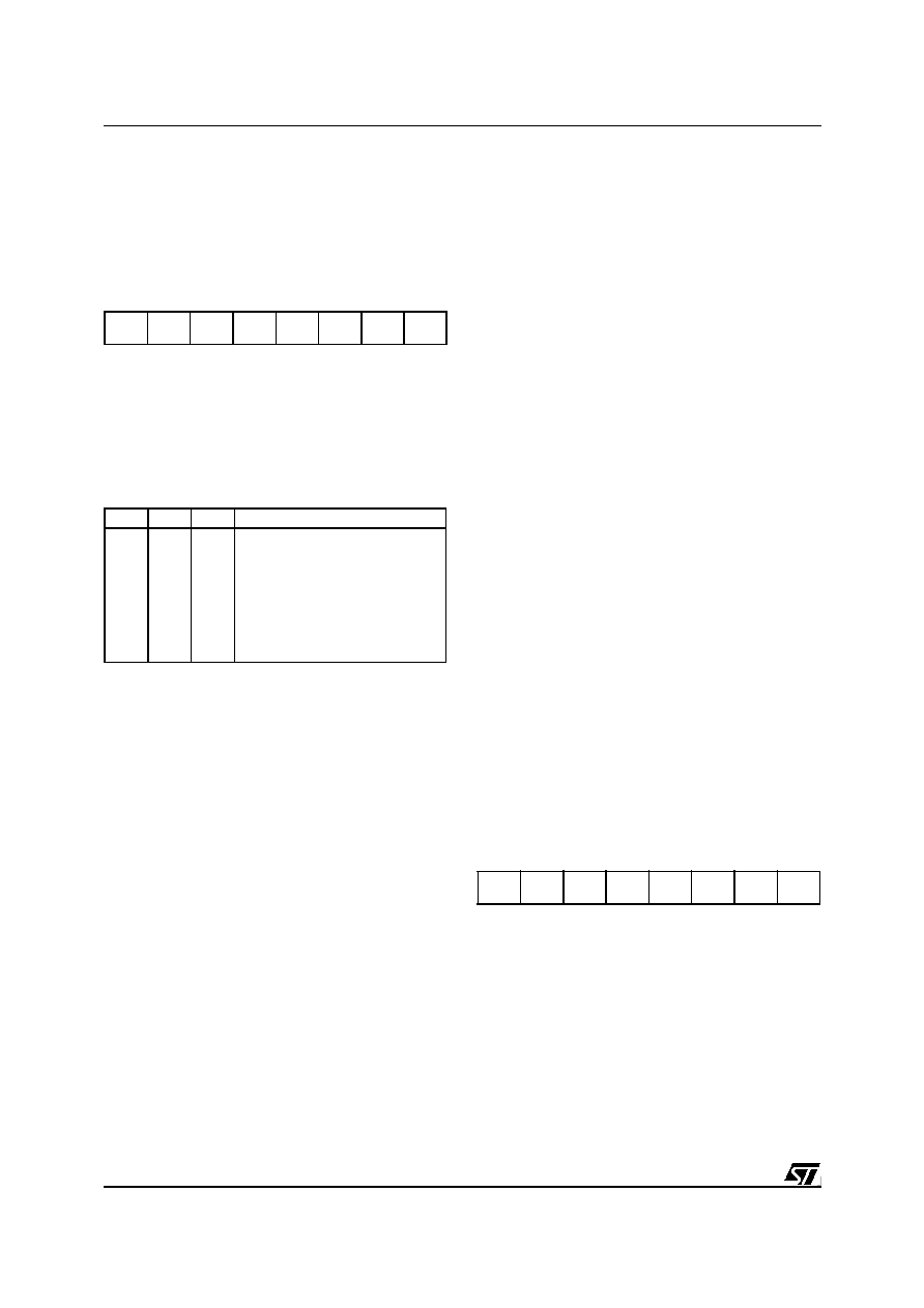
202/230
ST92163 - A/D CONVERTER (A/D)
A/D CONVERTER (Cont'd)
8.6.4 Register Description
A/D CONTROL LOGIC REGISTER (ADCLR)
R241 - Read/Write
Register Page: 62
Reset value: 0000 0000 (00h)
This 8-bit register manages the A/D logic opera-
tions. Any write operation to it will cause the cur-
rent conversion to be aborted and the logic to be
re-initialized to the starting configuration.
Bit 7:5 = C[2:0]:
Channel Address.
These bits are set and cleared by software. They
select channel
i
conversion as follows:
Bit 4 = FS:
Fast/Slow
.
This bit is set and cleared by software.
0: Fast mode. Single conversion time: 78 x
INTCLK (5.75µs at INTCLK = 12 MHz)
1: Slow mode. Single conversion time: 138 x
INTCLK (11.5µs at INTCLK = 12 MHz)
Note: Fast conversion mode is only allowed for in-
ternal speeds which do not exceed 12 MHz.
Bit 3 = TRG:
External/Internal Trigger Enable
.
This bit is set and cleared by software.
0: External/Internal Trigger disabled.
1: Either a negative (falling) edge on the EXTRG
pin or an On Chip Event
writes a "1" into the
STR bit, enabling start of conversion.
Note: Triggering by on chip event is available on
devices with the multifunction timer (MFT) periph-
eral.
Bit 2 = POW:
Power Enable
.
This bit is set and cleared by software.
0: Disables all power consuming logic.
1: Enables the A/D logic and analog circuitry.
Bit 1 = CONT:
Continuous/Single Mode Select
.
This bit it set and cleared by software.
0: Single mode: after the current conversion ends,
the STR bit is reset by hardware and the con-
verter logic is put in a wait status. To start anoth-
er conversion, the STR bit has to be set by soft-
ware or hardware.
1: Select Continuous Mode, a continuous flow of
A/D conversions on the selected channel, start-
ing when the STR bit is set.
Bit 0 = STR:
Start/Stop
.
This bit is set and cleared by software. It is also set
by hardware when the A/D is synchronized with an
external/internal trigger.
0: Stop conversion on channel i. An interrupt is
generated if the STR was previously set and the
AD-INT bit is set.
1: Start conversion on channel i
WARNING: When accessing this register, it is rec-
ommended to keep the related A/D interrupt chan-
nel masked or disabled to avoid spurious interrupt
requests.
A/D CHANNEL
i
DATA REGISTER (ADDTR)
R240 - Read/Write
Register Page: 62
Reset value: undefined
The result of the conversion of the selected chan-
nel is stored in the 8-bit ADDTR, which is reloaded
with a new value every time a conversion ends.
7
0
C2
C1
C0
FS
TRG POW CONT STR
C2
C1
C0
Channel Enabled
0
0
0
0
1
1
1
1
0
0
1
1
0
0
1
1
0
1
0
1
0
1
0
1
Channel 0
Channel 1
Channel 2
Channel 3
Channel 4
Channel 5
Channel 6
Channel 7
7
0
R.7
R.6
R.5
R.4
R.3
R.2
R.1
R.0

203/230
ST92163 - ON-CHIP PERIPHERALS
A/D CONVERTER (Cont'd)
A/D INTERRUPT REGISTER (ADINT)
Register Page: 62
R242 - Read/write
Reset value: 0000 0001 (01h)
Bit 7:1 = Reserved.
Bit 0 = AD-INT:
AD Converter Interrupt Enable
.
This bit is set and cleared by software. It allows the
interrupt source to be switched between the A/D
Converter and an external interrupt pin (See Inter-
rupts chapter).
0: A/D Interrupt disabled. External pin selected as
interrupt source.
1: A/D Interrupt enabled
7
0
-
-
-
-
-
-
-
AD-INT
204/230
ST92163 - ELECTRICAL CHARACTERISTICS
9 ELECTRICAL CHARACTERISTICS
The ST92163 device contains circuitry to protect
the inputs against damage due to high static volt-
age or electric field. Nevertheless it is advised to
take normal precautions and to avoid applying to
this high impedance voltage circuit any voltage
higher than the maximum rated voltages. It is rec-
ommended for proper operation that V
IN
and V
OUT
be constrained to the range:
V
SS
(
V
IN
or V
OUT
)
V
DD
To enhance reliability of operation, it is recom-
mended to connect unused inputs to an appropri-
ate logic voltage level such as V
SS
or V
DD
.
All the voltages in the following table, are refer-
enced to V
SS
.
ABSOLUTE MAXIMUM RATINGS
Note: Stresses above those listed as "absolute maximum ratings" may cause permanent damage to the device. This is a stress rating only
and functional operation of the device at these conditions is not implied. Exposure to maximum rating conditions for extended periods may
affect device reliability. All voltages are referenced to V
SS
RECOMMENDED OPERATING CONDITIONS
(Normal Voltage Mode, all devices)
Note 1. 1MHz when A/D is used
RECOMMENDED OPERATING CONDITIONS
(Low Voltage Modes, devices with suffix L or V))
Note 1. 1MHz when A/D is used
Symbol
Parameter
Value
Unit
V
DD
Supply Voltage
≠ 0.3 to +7.0
V
V
I
Input Voltage
≠ 0.3 to V
DD
+0.3
V
V
AI
Analog Input Voltage (A/D Converter)
V
SS
- 0.3 to V
DD
+0.3
AV
SS
- 0.3 to AV
DD
+0.3
V
V
O
Output Voltage
≠ 0.3 to V
DD
+0.3
V
T
STG
Storage Temperature
≠ 55 to + 150
∞
C
I
INJ
Pin Injection Current Digital and Analog Input
-5 to +5
mA
Maximum Accumulated Pin injection Current in the device
-50 to +50
mA
AV
DD
A/D Converter Analog Reference
V
DD
-0.3 to V
DD
+0.3
V
AV
SS
A/D Converter V
SS
V
SS
-0.3 to V
SS
+0.3
V
Symbol
Parameter
Value
Unit
Min.
Max.
T
A
Operating Temperature
0
70
∞
C
V
DD
Operating Supply Voltage
4.0
5.5
V
f
INTCLK
Internal Clock Frequency @ 4.0V - 5.5V
0
(1)
24
MHz
Symbol
Parameter
Value
Unit
Min.
Max.
T
A
Operating Temperature
0
70
∞
C
V
DD
Operating Supply Voltage
3.0
4.0
V
f
INTCLK
Internal Clock Frequency @ 3.0V - 4.0V
8-MHz Low Voltage devices
(devices with suffix L)
0
(1)
8
MHz
16-MHz Low Voltage devices
(devices with suffix V)
0
(1)
16
MHz
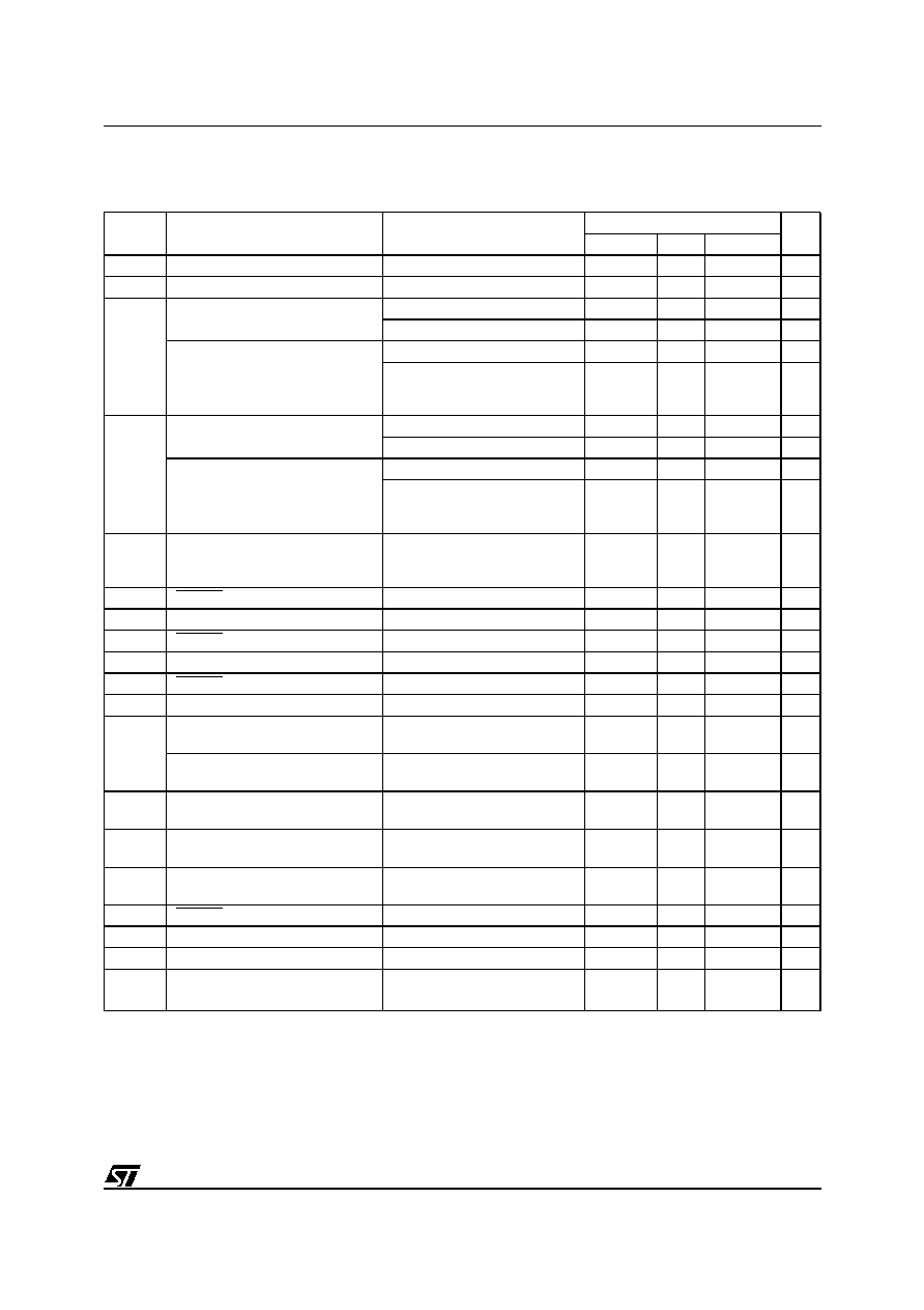
205/230
ST92163 - ELECTRICAL CHARACTERISTICS
DC ELECTRICAL CHARACTERISTICS
(V
DD
= 4.0 - 5.5V, T
A
= 0∞C + 70∞C, unless otherwise specified)
1
1
*For devices with suffix L or V, these characteristics are valid for V
DD
= 3.0 - 5.5V
Notes:
1. All I/O Ports are configured in bidirectional weak pull-up mode with no DC load external clock pin (OSCIN) is driven by square wave external
clock. No peripheral working.
2. Hysteresis voltage between switching levels: characterization results - not tested.
Symbol
Parameter
Test Conditions
Value
Unit
Min.
Typ.
Max.
V
IHCK
*
Clock Input High Level
External Clock
0.7 V
DD
V
DD
+ 0.3
V
V
ILCK
*
Clock Input Low Level
External Clock
≠ 0.3
0.3 V
DD
V
V
IH
*
Input High Level
P0[7:0], P1[7:0], P6[5:2],P6.7
TTL
2.0
V
DD
+ 0.3
V
CMOS
0.7 V
DD
V
DD
+ 0.3
V
Input High Level
Schmitt Trigger
P3[7:0], P4[3:0],P5[7:0], P6[1:0],
P6.6
Input threshold
TBD
TBD
V
Input Voltage Range
TBD
TBD
V
V
IL
*
Input Low Level
P0[7:0], P1[7:0], P6[5:2], P6.7
TTL
≠ 0.3
0.8
V
CMOS
≠ 0.3
0.3 V
DD
V
Input Low Level
Schmitt Trigger
P3[7:0], P4[3:0],P5[7:0], P6[1:0],
P6.6
Input threshold
TBD
TBD
V
Input Voltage Range
TBD
TBD
V
V
HYS
2
Input Hysteresis Schmitt trigger
P3[7:0], P4[3:0],P5[7:0], P6[1:0],
P6.6
TBD
TBD
V
IHRS
*
RESET Input High Level
Input threshold
0.5 V
DD
0.85 V
DD
V
Input Voltage Range
0.85 V
DD
V
DD
+ 0.3
V
ILRS
*
RESET Input Low Level
Input threshold
0.2 V
DD
0.6 V
DD
V
Input Voltage Range
-0.3
0.2 V
DD
V
HYRS
*
RESET Input Hysteresis
0.3
1.5
V
V
OH
*
Output High Level
Push Pull, Iload = ≠ 0.8mA
V
DD
≠ 0.8
V
V
OL
Output Low Level
Push Pull or Open Drain,
Iload = 1.6mA
0.4
V
Output Low Level high sink pins
(Port 6)
Iload = 10mA
1
V
I
WPU
Weak Pull-up Current
Bidirectional Weak Pull-up,
V
OL
= 0V
≠ 40
≠ 200
≠ 420
µ
A
I
APU
Active Pull-up Current,
for INT0 and INT7 only
V
IN
< 0.8V, under Reset
≠ 40
≠ 200
≠ 420
µ
A
I
LKIO
*
I/O Pin Input Leakage
Input/Tri-State,
0V < V
IN
< V
DD
≠ 10
+ 10
µ
A
I
LKRS
*
RESET Pin Input Leakage
0V < V
IN
< V
DD
≠ 10
+ 10
µ
A
I
LKA/D
*
A/D Conv. Input Leakage
≠ 3
+ 3
µ
A
I
LKAP
*
Active Pull-up Input Leakage
0V < V
IN
< 0.8V
≠ 10
+ 10
µ
A
I
LKOS
*
OSCIN Pin Input Leakage
0V < V
IN
< V
DD
±
10
µ
A
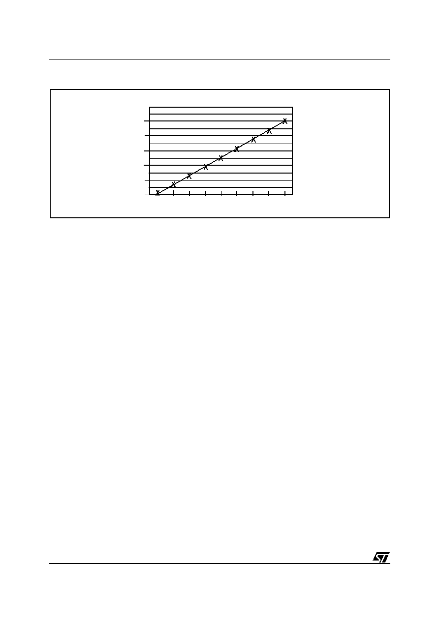
206/230
ST92163 - ELECTRICAL CHARACTERISTICS
Figure 90. Typical V
OL
at V
DD
=5V (high current)
0
0.1
0.2
0.3
0.4
0.5
0.6
2
4
6
8
10
12
14
16
Vol [V] at V
DD
= 5.0V and T= 25∞C
V
OL
[V
]
I
OL
[mA]
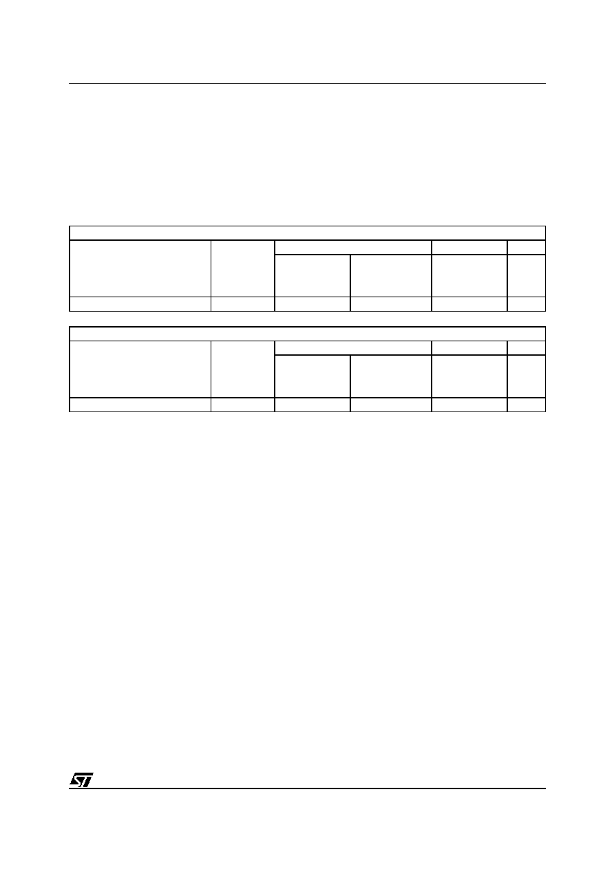
207/230
ST92163 - ELECTRICAL CHARACTERISTICS
INPUT/OUTPUT SPEED LIMITATIONS
Special care must be taken when using fast exter-
nal signalling with the ST92163 because the load
capacitance must be reduced to the minimum.
Therefore, it is recommended to use FAST mode
1)
or external buffering to avoid speed problems.
The following table will help you to select either
FAST or SLOW mode depending on the speed re-
quired. For instance, if you need to use the SCI in
Synchronous mode at 3 Mb/s, you must use FAST
mode or external buffering.
Since ROM devices are slightly slower than OTP
devices, to select between FAST or SLOW mode,
it is important to use the given values and not to
take into account the behaviour of a few samples.
Note 1: SLOW mode and FAST mode are selected through the BSZ bit in the EMR1 register (described
in the External Memory Interface chapter: 0 = SLOW mode; 1 = FAST mode). It is important to note that
all I/Os will be impacted by the Slow or Fast Mode selection.
Input/Output Rising/Falling edges in SLOW MODE
1)
Parameter
Conditions
Typ. Max.
Unit
(OTP device)
V
DD
= 5 V
T
A
= 20∞ C
(ROM device)
V
DD
= 5 V
T
A
= 20∞ C
(ROM & OTP)
V
DD
= 4.0 V
T
A
= 70∞ C
Rising and falling edges
C
Load
= 50 pf
35
50
100
ns
Input/Output Rising/Falling edges in FAST MODE
1)
Parameter
Conditions
Typ. Max.
Unit
(OTP device)
V
DD
= 5 V
T
A
= 20∞ C
(ROM device)
V
DD
= 5 V
T
A
= 20∞ C
(ROM & OTP)
V
DD
= 4.0 V
T
A
= 70∞ C
Rising and falling edges
C
Load
= 50 pf
14
14
30
ns
208/230
ST92163 - ELECTRICAL CHARACTERISTICS
AC ELECTRICAL CHARACTERISTICS
(V
DD
= 4.0 - 5.5V, T
A
= 0∞C + 70∞C, unless otherwise specified)
(V
DD
= 3.0 - 3.3 V, T
A
= 0∞C + 70∞C
)
Note: All I/O Ports are configured in bidirectional weak pull-up mode with no DC load, external clock pin (OSCIN) is driven by square wave
external clock
(1)
External pull-up (1.5 Kohms connected to USBV
CC
); Operating conditions: V
DD
= 4.0 - 5.25V; T
A
= 25∞C
Symbol
Parameter
Conditions
V
DD
= 4.0V - 5.5V
(Normal Mode)
Unit
TYP
MAX
I
DD
Run Mode Current @ 24 MHz
No transfer on USB
40
mA
Transfer on USB at 50%
of bandwidth
55
Transfer on USB at maxi-
mum bandwidth
72
85
I
WFI
WFI Mode @ 24 MHz
20
mA
I
HALT
HALT Mode Current
100
µ
A
I
SUSP
USB Suspend mode current
(1)
450
µA
Symbol
Parameter
V
DD
= 3.0 - 3.3V
(Low Voltage Mode)
Unit
TYP
MAX
I
DD
Run Mode Current
1.2
1.4
mA/MHz
I
WFI
WFI Mode
0.3
0.4
mA/MHz
I
HALT
HALT Mode Current
100
µ
A

209/230
ST92163 - ELECTRICAL CHARACTERISTICS
ELECTRICAL CHARACTERISTICS (Cont'd)
*
Not available on devices with suffix L, V or E
**Guaranteed by design
N/A = not applicable
Low Voltage Detector Reset Electrical Specifications*
Symbol
Parameter
Conditions
Min Typ
Max
Unit
V
IT+
LV Reset Trigger
V
DD
rising edge
INTCLK = 24MHz
3.5
3.7
3.9
V
V
IT-
LV Reset Trigger
V
DD
Falling edge
3.3
3.5
3.7
V
V
Hyst
Hysteresis **
150
200
250
mV
V
LVDMIN
Min. LVD Operating Voltage
2.0
V
t
g(VDD)
Filtered glitch delay on V
DD
Not detected by the LVD
50
ns
I
2
C Interface Electrical specifications
Parameter
Symbol
Standard mode I2C
Fast mode I2C
Unit
Min
Max
Min
Max
Low level input voltage:
fixed input levels
V
DD
-related input levels
V
IL
-0.5
-0.5
1.5
0.3 V
DD
-0.5
-0.5
1.5
0.3 V
DD
V
High level input voltage:
V
DD
-related input levels
0.7 V
DD
V
DD
+0.5
0.7 V
DD
V
DD
+0.5
V
Hysteresis of Schmitt trigger inputs
fixed input levels
V
DD
-related input levels
V
HYS
N/A
N/A
N/A
N/A
0.2
0.05 V
DD
V
Pulse width of spikes which must be sup-
pressed by the input filter
T
SP
N/A
N/A
0 ns
50 ns
ns
Low level output voltage (open drain and open
collector)
at 3 mA sink current
at 6 mA sink current
V
OL1
V
OL2
0
N/A
0.4
N/A
0
0
0.4
0.6
V
Output fall time from VIH min to VIL max with a
bus capacitance from 10 pF to 400 pF
with up to 3 mA sink current at V
OL1
with up to 6 mA sink current at V
OL2
T
OF
N/A
250
N/A
20+0.1Cb
20+0.1Cb
250
250
ns
Input current each I/O pin with an input voltage
between 0.4V and 0.9 V
DD
max
I
- 10
10
-10
10
µ
A
Capacitance for each I/O pin
C
10
10
pF
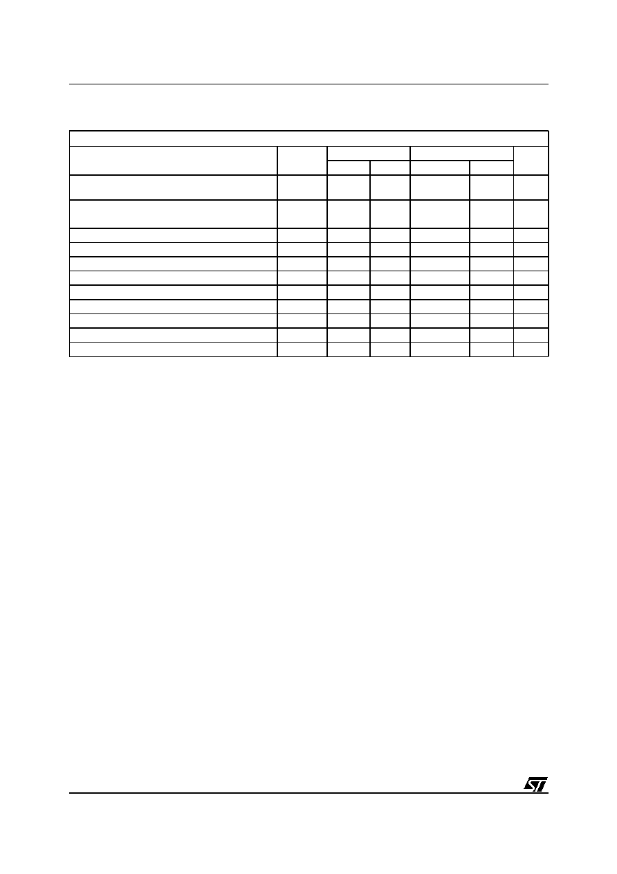
210/230
ST92163 - ELECTRICAL CHARACTERISTICS
ELECTRICAL CHARACTERISTICS (Cont'd)
1)The device must internally provide a hold time of at least 300 ns for the SDA signal in order to bridge the unde-
fined region of the falling edge of SCL
2)The maximum hold time of the START condition has only to be met if the interface does not stretch the low period
of SCL signal
Cb = total capacitance of one bus line in pF
I
2
C Bus Timings
Parameter
Symbol
Standard I
2
C
Fast I
2
C
Unit
Min
Max
Min
Max
Bus free time between a STOP and START con-
dition
T
BUF
4.7
1.3
m
s
Hold time START condition. After this period,
the first clock pulse is generated
T
HD:STA
4.0
0.6
µ
s
LOW period of the SCL clock
T
LOW
4.7
1.3
µ
s
HIGH period of the SCL clock
T
HIGH
4.0
0.6
µ
s
Set-up time for a repeated START condition
T
SU:STA
4.7
0.6
µ
s
Data hold time
T
HD:DAT
0 (1)
0 (1)
0.9(2)
ns
Data set-up time
T
SU:DAT
250
100 ns
Rise time of both SDA and SCL signals
T
R
1000
20+0.1Cb
300
ns
Fall time of both SDA and SCL signals
TF
300
20+0.1Cb
300
ns
Set-up time for STOP condition
T
SU
:
STO
4.0
0.6 ns
Capacitive load for each bus line
Cb
400
400
pF
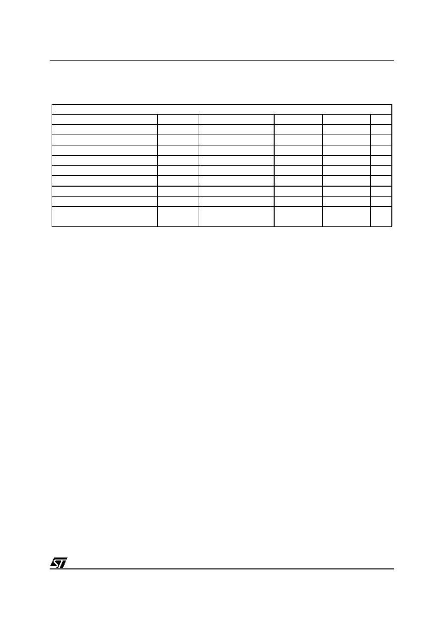
211/230
ST92163 - ELECTRICAL CHARACTERISTICS
USB INTERFACE: DC CHARACTERISTICS
(V
DD
= 4.0 - 5.5V, T
A
= 0∞C + 70∞C, unless otherwise specified)
RL is the load connected on the USB drivers.
All voltages are measured from the local ground potential (USBGND).
USB Interface: DC Electrical Characteristics
Parameter
Symbol
Conditions
Min.
Max.
Unit
Inputs Levels:
Differential Input Sensitivity
V
DI
I(D+, D-)
0.2
V
Differential Common Mode Range
V
CM
Includes V
DI
range
0.8
2.5
V
Single Ended Receiver Threshold
V
SE
0.8
2.0
V
Output Levels
Static Output Low
V
OL
RL of 1.5K ohms to 3.6v
0.3
V
Static Output High
V
OH
RL of 15K ohm to GND
2.8
3.6
V
USBVCC: voltage level
USB
V
V
DD
=5V
2.97
3.63
V
Hi-Z State Data Line Leakage
I
LO
0 V < Vin < 3.3 V
(Regulator ON)
-10
+10
µ
A
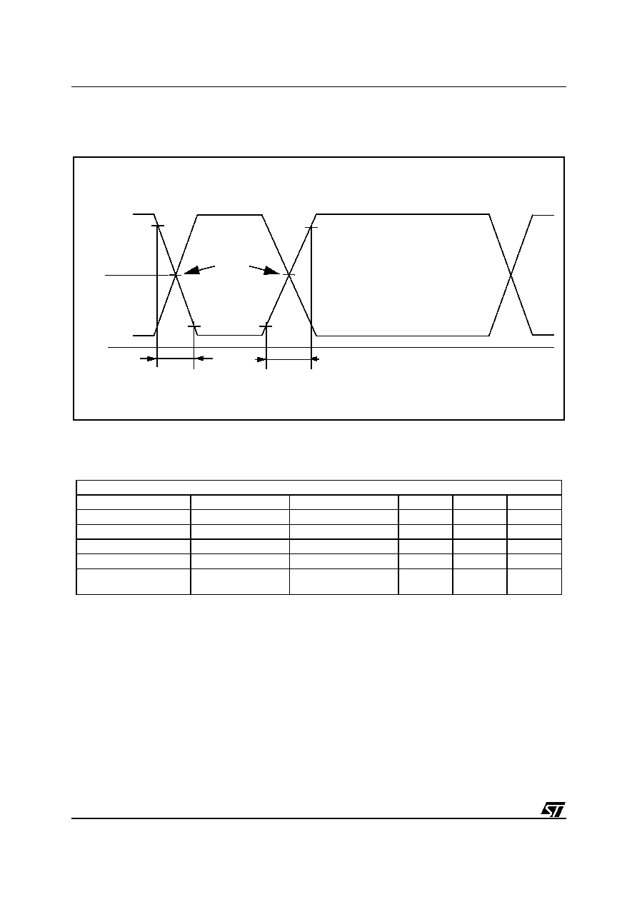
212/230
ST92163 - ELECTRICAL CHARACTERISTICS
ELECTRICAL CHARACTERISTICS (Cont'd)
Figure 91. USB Interface: Data signal rise and fall time
USB INTERFACE: FULL SPEED CHARACTERISTICS
(V
DD
= 4.0 - 5.5V, T
A
= 0∞C + 70∞C, unless otherwise specified)
1)
Measured from 10% to 90% of the data signal
Differential
Data Lines
USBGND
tf
tr
Crossover
points
VCRS
USB Interface: Full speed electrical characteristics
Parameter
Symbol
Conditions
Min
Max
Unit
Driver characteristics:
Rise time
tr
CL=50 pF
1)
4
20
ns
Fall Time
tf
CL=50 pF
1)
4
20
ns
Rise/ Fall Time matching
trfm
tr/tf
90
110
%
Output signal Crossover
Voltage
VCRS
1.3
2.0
V
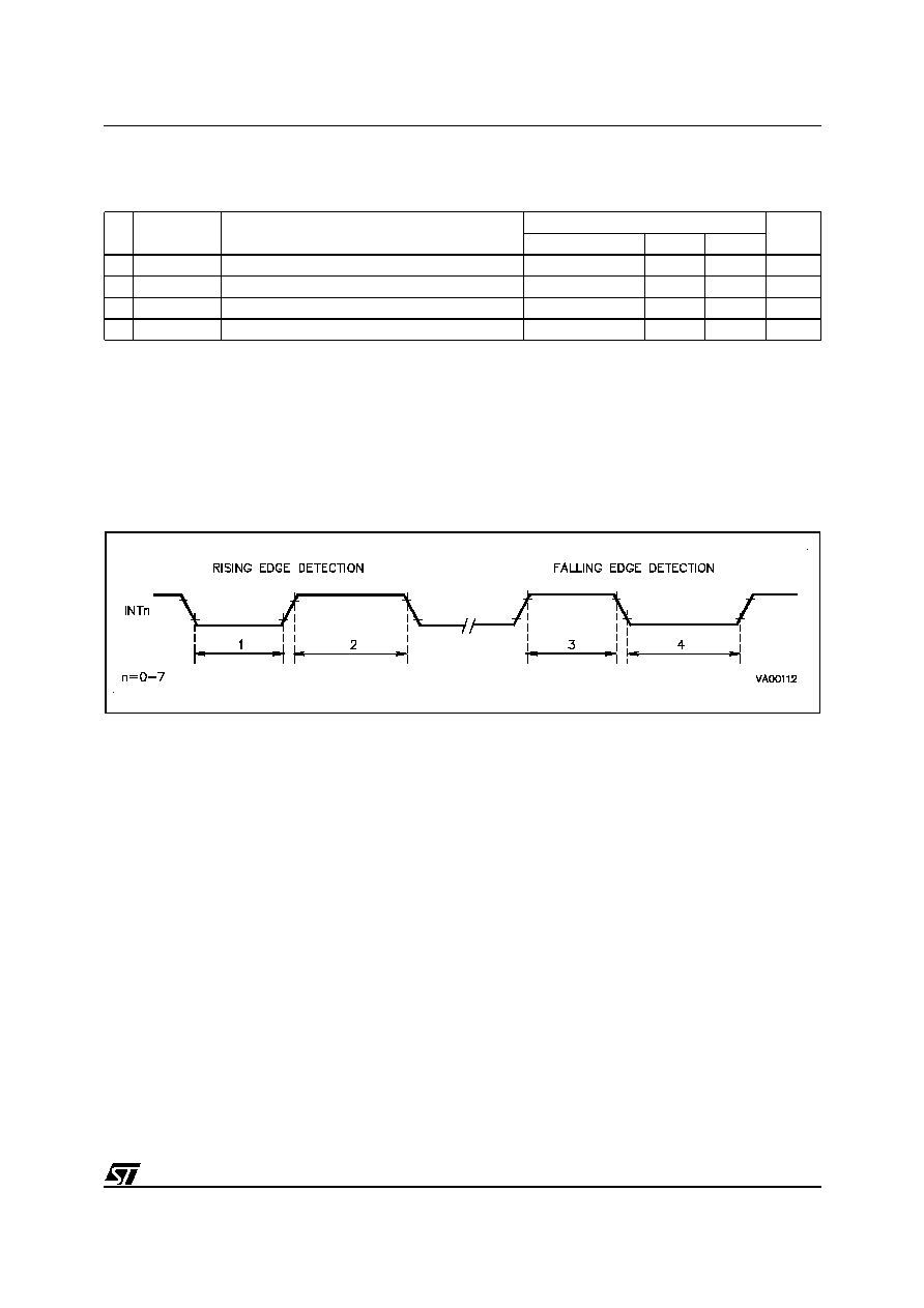
213/230
ST92163 - ELECTRICAL CHARACTERISTICS
EXTERNAL INTERRUPT TIMING TABLE
(V
DD
= 3.0 - 5.5V
(1)
, T
A
= 0∞C + 70∞C, C
Load
= 50pF, f
INTCLK
= 24MHz, unless otherwise specified)
Note: The value in the left hand column shows the formula used to calculate the timing minimum or maximum from the oscillator clock period.
The value in the right hand two columns show the timing minimum and maximum for an internal clock at 24MHz (INTCLK).
(1) 3.0 - 4.0V voltage range is only available on devices with suffix L or V, with different frequency limitations (L: 8 MHz, V: 16 MHz)
(2) Formula guaranteed by design.
Legend:
Tck = INTCLK period = OSCIN period when OSCIN is not divided by 2;
2 x OSCIN period when OSCIN is divided by 2;
OSCIN period x PLL factor when the PLL is enabled.
EXTERNAL INTERRUPT TIMING
N∞
Symbol
Parameter
Value (Note)
Unit
Formula
(2)
Min
Max
1
TwINTLR
Low Level Pulse Width in Rising Edge Mode
Tck+10
50
ns
2
TwINTHR
High Level Pulse Width in Rising Edge Mode
Tck+10
50
ns
3
TwINTHF
High Level Pulse Width in Falling Edge Mode
Tck+10
50
ns
4
TwINTLF
Low Level Pulse Width in Falling Edge Mode
Tck+10
50
ns
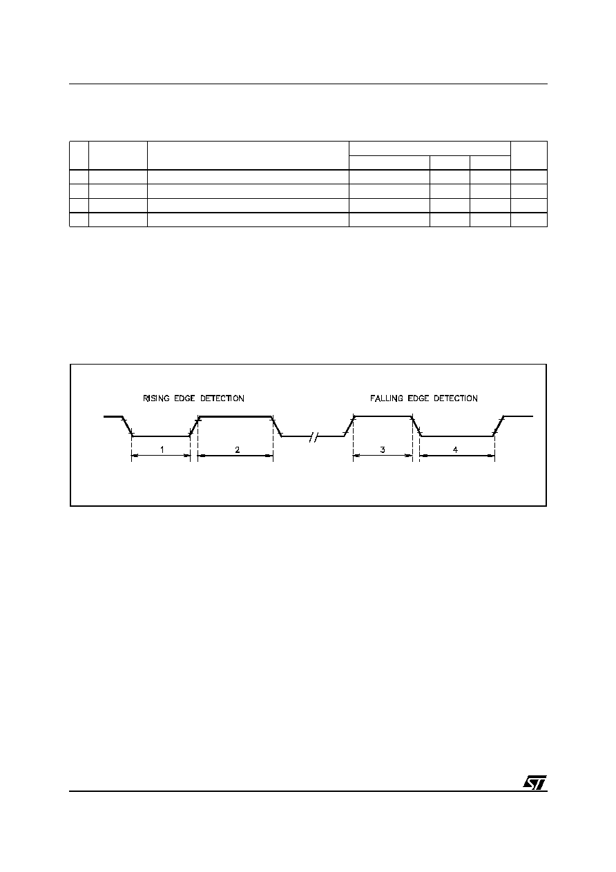
214/230
ST92163 - ELECTRICAL CHARACTERISTICS
WAKE-UP MANAGEMENT TIMING TABLE
(V
DD
= 3.0 - 5.5V
(1)
, T
A
= 0∞C + 70∞C, C
Load
= 50pF, f
INTCLK
= 24MHz, unless otherwise specified)
Note: The value in the left hand column shows the formula used to calculate the timing minimum or maximum from the oscillator clock period.
The value in the right hand two columns show the timing minimum and maximum for an internal clock at 24MHz (INTCLK).
The given data are related to Wake-up Management Unit used in External Interrupt mode.
(1) 3.0 - 4.0V voltage range is only available on devices with suffix L or V, with different frequency limitations (L: 8 MHz, V: 16 MHz)
(2) Formula guaranteed by design.
Legend:
Tck = INTCLK period = OSCIN period when OSCIN is not divided by 2;
2 x OSCIN period when OSCIN is divided by 2;
OSCIN period x PLL factor when the PLL is enabled.
WAKE-UP MANAGEMENT TIMING
N∞
Symbol
Parameter
Value (Note)
Unit
Formula
(2)
Min
Max
1
TwWKPLR
Low Level Pulse Width in Rising Edge Mode
Tck+10
50
ns
2
TwWKPHR
High Level Pulse Width in Rising Edge Mode
Tck+10
50
ns
3
TwWKPHF
High Level Pulse Width in Falling Edge Mode
Tck+10
50
ns
4
TwWKPLF
Low Level Pulse Width in Falling Edge Mode
Tck+10
50
ns
WKUPn
n=0
≠
15
215/230
ST92163 - ELECTRICAL CHARACTERISTICS
RCCU CHARACTERISTICS
(V
DD
= 3.0 - 5.5V
(1)
, T
A
= 0∞C + 70∞C, C
Load
= 50pF, f
INTCLK
= 24MHz, unless otherwise specified)
(1) 3.0 - 4.0V voltage range is only available on devices with suffix L or V, with different frequency limitations (L: 8 MHz, V: 16 MHz)
RCCU TIMING TABLE
(V
DD
= 3.0 - 5.5V
(1)
, T
A
= 0∞C + 70∞C, C
Load
= 50pF, f
INTCLK
= 24MHz, unless otherwise specified)
(1) 3.0 -4.0V voltage range is only available on devices with suffix L or V, with different frequency limitations (L: 8 MHz, V:16 MHz)
(2) Depending on the delay between rising edge of RESETN pin and the first rising edge of CLOCK1, the value can differ from the typical
value for +/- 1 CLOCK1 cycle.
Legend: T
osc
= OSCIN clock cycles
PLL CHARACTERISTICS
(V
DD
= 3.0 - 5.5V
(1)
, T
A
= 0∞C + 70∞C, C
Load
= 50pF, f
INTCLK
= 24MHz, unless otherwise specified)
(1) 3.0 - 4.0V voltage range is only available on devices with suffix L or V, with different frequency limitations (L: 8 MHz, V: 16 MHz)
(2) Measured at 24MHz (INTCLK). Guaranteed by Design Characterisation (not tested).
Legend: Tosc = OSCIN clock cycles
Symbol
Parameter
Comment
Value (Note)
Unit
Min
Typ
Max
V
IHRS
RESET Input High Level
0.85 x V
DD
V
DD
+ 0.3
V
V
ILRS
RESET Input Low Level
≠ 0.3
0.2 x V
DD
V
V
HYRS
RESET Input Hysteresis
0.3
0.9
1.5
V
I
LKRS
RESET Pin Input Leakage
0V < V
IN
< V
DD
≠ 10
+ 10
µ
A
Symbol
Parameter
Comment
Value (Note)
Unit
Min
Typ
Max
T
FRS
RESET Input Filtered Pulse
50
20
ns
µ
s
T
RSPH
(2)
RESET Phase duration
20400 x T
osc
µ
s
T
STR
STOP Restart duration
DIV2 = 0
DIV2 = 1
10200 x T
osc
20400 x T
osc
µ
s
Symbol
Parameter
Comment
Value (Note)
Unit
Min
Typ
Max
F
XTL
Crystal Reference Frequency
3
8
MHz
F
VCO
VCO Operating Frequency
9
48
MHz
T
PLK
Lock-in Time
1000 x Tosc
µ
s
PLL Jitter
0
850
(2)
ps
216/230
ST92163 - ELECTRICAL CHARACTERISTICS
OSCILLATOR CHARACTERISTICS
(V
DD
= 3.0 - 5.5V
(1)
, T
A
= 0∞C + 70∞C, C
Load
= 50pF, f
INTCLK
= 24MHz, unless otherwise specified)
(1) 3.0 - 4.0V voltage range is only available on devices with suffix L or V, with different frequency limitations (L: 8 MHz, V: 16 MHz)
Symbol
Parameter
Comment
Value (Note)
Unit
Min
Typ
Max
F
OSC
Crystal Frequency
Fundamental mode crystal only
3
8
MHz
g
m
Oscillator
V
DD
= 4.0 - 5.5 V
0.77
1.5
2.4
mA/V
V
DD
= 3.0 - 4.0 V
0.5
0.73
1.47
mA/V
V
IHCK
Clock Input High Level
External Clock
0.8 x V
DD
V
DD
+ 0.3
V
V
ILCK
Clock Input Low Level
External Clock
≠ 0.3
0.2 x V
DD
V
I
LKOS
OSCIN/OSCOUT Pin
Input Leakage
0V < V
IN
< V
DD
(HALT/STOP)
≠ 1
+ 1
µ
A
T
STUP
Oscillator Start-up Time
V
DD
= 4.0 - 5.5 V
5
ms
V
DD
= 3.0 - 4.0 V
20
ms
217/230
ST92163 - ELECTRICAL CHARACTERISTICS
EXTERNAL BUS TIMING TABLE
(V
DD
= 3.0 - 5.5V
(1)
, T
A
= 0∞C + 70∞C, C
Load
= 50pF, f
INTCLK
= 24MHz, unless otherwise specified)
Note: The value in the left hand column shows the formula used to calculate the timing minimum or maximum from the oscillator clock period,
prescaler value and number of wait cycles inserted.
The values in the right hand two columns show the timing minimum and maximum for an external clock at 24MHz, prescaler value of zero
and zero wait states.
(1) 3.0 - 4.0V voltage range is only available on devices with suffix L or V, with different frequency limitations (L: 8 MHz, V: 16 MHz)
Legend:
Tck = INTCLK period = OSCIN period when OSCIN is not divided by 2;
2 x OSCIN period when OSCIN is divided by 2;
OSCIN period x PLL factor when the PLL is enabled.
TckH = INTCLK high pulse width (normally = Tck/2, except when INTCLK = OSCIN, in which case it is OSCIN high pulse width)
TckL = INTCLK low pulse width (normally = Tck/2, except when INTCLK = OSCIN, in which case it is OSCIN low pulse width)
P = clock prescaling value (=PRS; division factor = 1+P)
Wa = wait cycles on AS; = max (P, programmed wait cycles in EMR2, requested wait cycles with WAIT)
Wd = wait cycles on DS; = max (P, programmed wait cycles in WCR, requested wait cycles with WAIT)
N∞
Symbol
Parameter
Value (Note)
Unit
Formula
Min
Max
1
TsA (AS)
Address Set-up Time before AS
Tck x Wa+TckH-9
12
ns
2
ThAS (A)
Address Hold Time after AS
TckL-4
17
ns
3
TdAS (DR)
AS
to Data Available (read)
Tck x (Wd+1)+3
45
ns
4
TwAS
AS Low Pulse Width
Tck x Wa+TckH-5
16
ns
5
TdAz (DS)
Address Float to DS
0
0
ns
6
TwDS
DS Low Pulse Width
Tck x Wd+TckH-5
16
ns
7
TdDSR (DR)
DS
to Data Valid Delay (read)
Tck x Wd+TckH+4
25
ns
8
ThDR (DS)
Data to DS
Hold Time (read)
7
7
ns
9
TdDS (A)
DS
to Address Active Delay
TckL+11
32
ns
10
TdDS (AS)
DS
to AS
Delay
TckL-4
17
ns
11
TsR/W (AS)
RW Set-up Time before ASN
Tck x Wa+TckH-17
4
ns
12
TdDSR (R/W)
DS
to RW and Address Not Valid Delay
TckL-1
20
ns
13
TdDW (DSW)
Write Data Valid to DS
Delay
-16
-16
ns
14
TsD(DSW)
Write Data Set-up before DS
Tck x Wd+TckH-16
5
ns
15
ThDS (DW)
Data Hold Time after DS
(write)
TckL-3
18
ns
16
TdA (DR)
Address Valid to Data Valid Delay (read)
Tck x (Wa+Wd+1)+TckH-7
55
ns
17
TdAs (DS)
AS
to DS
Delay
TckL-6
15
ns
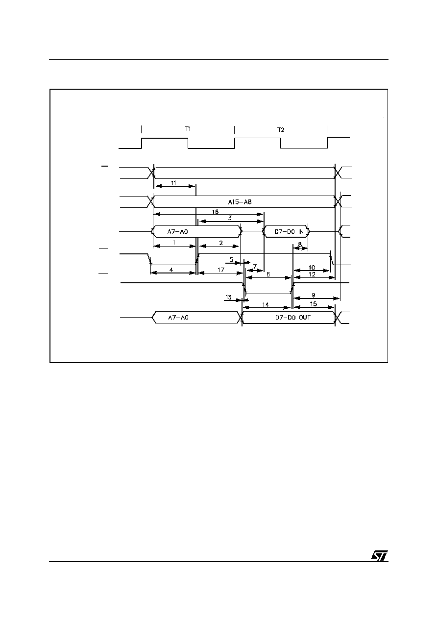
218/230
ST92163 - ELECTRICAL CHARACTERISTICS
EXTERNAL BUS TIMING
CPUCLK
RW
PORT1
PORT0
(READ)
AS
DS
PORT0
(WRITE)
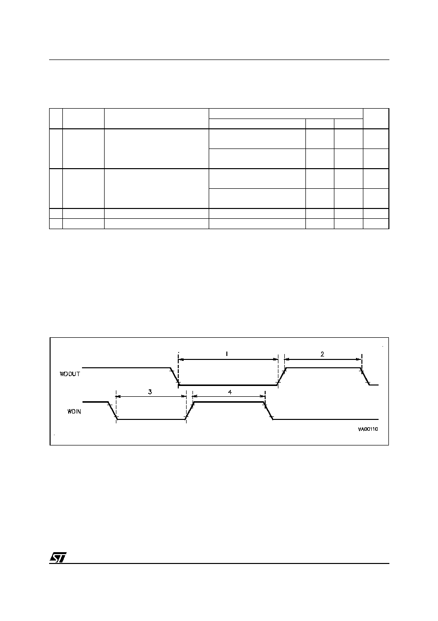
219/230
ST92163 - ELECTRICAL CHARACTERISTICS
WATCHDOG TIMING TABLE
(V
DD
= 3.0 - 5.5V
(1)
, T
A
= 0∞C + 70∞C, C
Load
= 50pF, f
INTCLK
= 24MHz, Push-pull output configuration,
unless otherwise specified)
Note: The value in the left hand column shows the formula used to calculate the timing minimum or maximum from the oscillator clock period,
watchdog prescaler and counter programmed values.
The value in the right hand two columns show the timing minimum and maximum for an internal clock (INTCLK) at 24MHz, with minimum and
maximum prescaler value and minimum and maximum counter value.
(1) 3.0 - 4.0V voltage range is only available on devices with suffix L or V, with different frequency limitations (L: 8 MHz, V: 16 MHz)
Legend:
Tck = INTCLK period = OSCIN period when OSCIN is not divided by 2;
2 x OSCIN period when OSCIN is divided by 2;
OSCIN period x PLL factor when the PLL is enabled.
Psc = Watchdog Prescaler Register content (WDTPR): from 0 to 255
Cnt = Watchdog Counter Registers content (WDTRH,WDTRL): from 0 to 65535
T
WDIN
= Watchdog Input signal period (WDIN)
WATCHDOG TIMING
N∞
Symbol
Parameter
Value (Note)
Unit
Formula
Min
Max
1
TwWDOL
WDOUT Low Pulse Width
4 x (Psc+1) x (Cnt+1) x Tck
167
2.8
ns
s
(Psc+1) x (Cnt+1) x T
WDIN
with T
WDIN
8 x Tck
333
ns
2
TwWDOH
WDOUT High Pulse Width
4 x (Psc+1) x (Cnt+1) x Tck
167
2.8
ns
s
(Psc+1) x (Cnt+1) x T
WDIN
with T
WDIN
8 x Tck
333
ns
3
TwWDIL
WDIN High Pulse Width
4 x Tck
167
ns
4
TwWDIH
WDIN Low Pulse Width
4 x Tck
167
ns
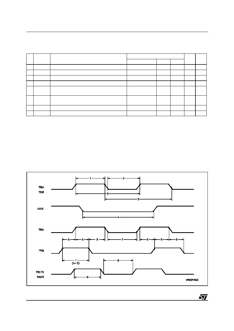
220/230
ST92163 - ELECTRICAL CHARACTERISTICS
MULTIFUNCTION TIMER EXTERNAL TIMING TABLE
(V
DD
= 3.0 - 5.5V
(1)
, T
A
= 0∞C + 70∞C, C
Load
= 50pF, f
INTCLK
= 24MHz, unless otherwise specified)
Note: The value in the left hand column shows the formula used to calculate the timing minimum or maximum from the oscillator clock period,
standard timer prescaler and counter programmed values.
The value in the right hand two columns show the timing minimum and maximum for an internal clock (INTCLK) at 24MHz.
(1) 3.0 - 4.0V voltage range is only available on devices with suffix L or V, with different frequency limitations (L: 8 MHz, V: 16 MHz)
(2) n = 1 if the input is rising OR falling edge sensitive
n = 3 if the input is rising AND falling edge sensitive
(3) In Autodiscrimination mode
Legend:
Tck = INTCLK period = OSCIN period when OSCIN is not divided by 2;
2 x OSCIN period when OSCIN is divided by 2;
OSCIN period x PLL factor when the PLL is enabled.
MULTIFUNCTION TIMER EXTERNAL TIMING
N∞
Symbol
Parameter
Value
Unit
Note
Formula
Min
Max
1
Tw
CTW
External clock/trigger pulse width
n x Tck
n x 42
-
ns
(2)
2
Tw
CTD
External clock/trigger pulse distance
n x Tck
n x 42
-
ns
(2)
3
Tw
AED
Distance between two active edges
3 x Tck
125
-
ns
4
Tw
GW
Gate pulse width
6 x Tck
250
-
ns
5
Tw
LBA
Distance between TINB pulse edge and the fol-
lowing TINA pulse edge
Tck
42
-
ns
(3)
6
Tw
LAB
Distance between TINA pulse edge and the fol-
lowing TINB pulse edge
0
-
ns
(3)
7
Tw
AD
Distance between two TxINA pulses
0
-
ns
(3)
8
Tw
OWD
Minimum output pulse width/distance
3 x Tck
125
-
ns
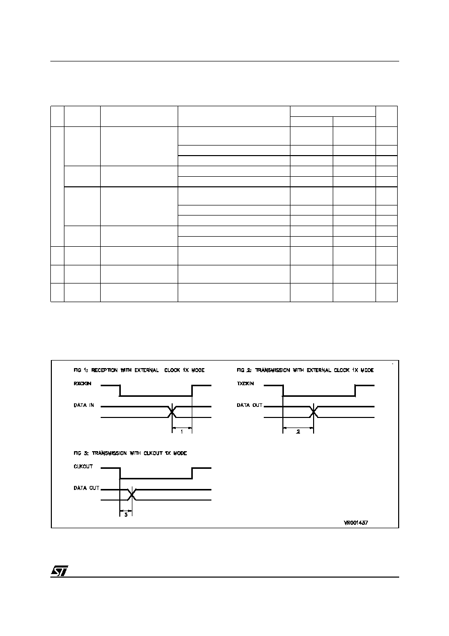
221/230
ST92163 - ELECTRICAL CHARACTERISTICS
SCI TIMING TABLE
(V
DD
= 3.0 - 5.5V
(1)
, T
A
= 0∞C + 70∞C, C
Load
= 50pF, f
INTCLK
= 24MHz, unless otherwise specified)
(1) 3.0 - 4.0V voltage range is only available on devices with suffix L or V, with different frequency limitations (L: 8 MHz, V: 16 MHz)
Legend:
Tck = INTCLK period = OSCIN period when OSCIN is not divided by 2;
2 x OSCIN period when OSCIN is divided by 2;
OSCIN period x PLL factor when the PLL is enabled.
SCI TIMING
N
∞
Symbol
Parameter
Condition
Value
Unit
Min
Max
F
RxCKIN
Frequency of RxCKIN
1x mode, V
DD
= 4.0 to 5.5V,
C
Load
= 30pF
f
INTCLK
/ 4
MHz
1x mode
f
INTCLK
/ 8
MHz
16x mode
f
INTCLK
/ 4
MHz
Tw
RxCKIN
RxCKIN shortest pulse
1x mode
2 x Tck
s
16x mode
2 x Tck
s
F
TxCKIN
Frequency of TxCKIN
1x mode, V
DD
= 4.0 to 5.5V,
C
Load
= 30pF
f
INTCLK
/ 4
1x mode
f
INTCLK
/ 8
MHz
16x mode
f
INTCLK
/ 4
MHz
Tw
TxCKIN
TxCKIN shortest pulse
1x mode
2 x Tck
s
16x mode
2 x Tck
s
1
Ts
DS
DS (Data Stable) before
rising edge of RxCKIN
1x mode reception with RxCKIN
Tck / 2
ns
2
Td
D1
TxCKIN to Data out
delay Time
1x mode transmission with external
clock C
Load
< 50pF
2.5 x Tck
ns
3
Td
D2
CLKOUT to Data out
delay Time
1x mode transmission with CLKOUT
TBD
ns
222/230
ST92163 - ELECTRICAL CHARACTERISTICS
A/D CONVERTER, EXTERNAL TRIGGER TIMING TABLE
(
V
DD
= 3.0 - 5.5V
(1)
;
T
A
= 0 to 70∞C; unless otherwise specified)
(1) 3.0 - 4.0V voltage range is only available on devices with suffix L or V, with different frequency limitations (L: 8 MHz, V: 16 MHz)
A/D CONVERTER. ANALOG PARAMETERS TABLE
(
V
DD
= 3.0 - 5.5V
(1)
;
T
A
= 0 to 70∞C; unless otherwise specified)
Notes: (*)
The values are expected at 25 Celsius degrees with
V
DD
= 5V
(**)
'LSBs', as used here, as a value of
V
DD
/256
(***) Characterized but not tested
(1)
3.0 - 4.0V voltage range is only available on devices with suffix L or V, with different frequency limitations (L: 8 MHz, V: 16 MHz)
(2)
including Sample time
(3)
it must be considered as the on-chip series resistance before the sampling capacitor
(4)
DNL ERROR= max {[V(i) -V(i-1)] / LSB-1}
INL ERROR= max {[V(i) -V(0)] / LSB-i}
ABSOLUTE ACCURACY= overall max conversion error
Symbol
Parameter
OSCIN divide by
2;min/max
OSCIN divide
by 1; min/max
Value
Unit
min
max
T
low
Pulse Width
1.5
INTCLK
ns
T
high
Pulse Distance
ns
T
ext
Period/fast Mode
78+1
INTCLK
µs
T
str
Start Conversion Delay
0.5
1.5
INTCLK
Parameter
Value
Unit
Note
typ (*)
min
max(***)
(**)
Analog Input Range
V
SS
V
DD
V
Conversion Time Fast/Slow
78/138
INTCLK
(2)
Sample Time Fast/Slow
51.5/87.5
INTCLK
Power-up Time
60
µs
Resolution
8
bits
Differential Non Linearity
0.5
1.5
LSBs
(4)
Integral Non Linearity
0.5
1.5
LSBs
(4)
Offset Error
0.5
1
Gain Error
0.5
1.5
Absolute Accuracy
1
2
LSBs
(4)
Input Resistance
1.5
Kohm
(3)
Hold Capacitance
1.92
pF

223/230
ST92163 - GENERAL INFORMATION
10 GENERAL INFORMATION
10.1 EPROM/OTP PROGRAMMING
The 20 Kbytes of EPROM/OTP of the ST92E163/
ST92T163 may be programmed using the
EPROM programming boards available from
STMicroelectronics.
EPROM Erasing
The EPROM of the windowed package of the
ST92E163 can be erased by exposure to Ultra-Vi-
olet light.
The erasure characteristic of the ST92E163 is
such that erasure begins when the memory is ex-
posed to light with wave lengths shorter than ap-
proximately 4000≈. It should be noted that sunlight
and some types of fluorescent lamps have wave-
lengths in the range 3000-4000≈. It is recom-
mended to cover the window of the ST92E163
packages by an opaque label to prevent uninten-
tional erasure problems when testing the applica-
tion in such an environment.
The recommended erasure procedure of the
EPROM is the exposure to short wave ultraviolet
light which have a wave-length 2537≈. The inte-
grated dose (i.e. U.V. intensity x exposure time) for
erasure should be a minimum of 15W-sec/cm2.
The erasure time with this dosage is approximate-
ly 30 minutes using an ultraviolet lamp with a
12000 mW/cm2 power rating. The device should
be placed within 2.5 cm (1 inch) of the lamp tubes
during erasure.
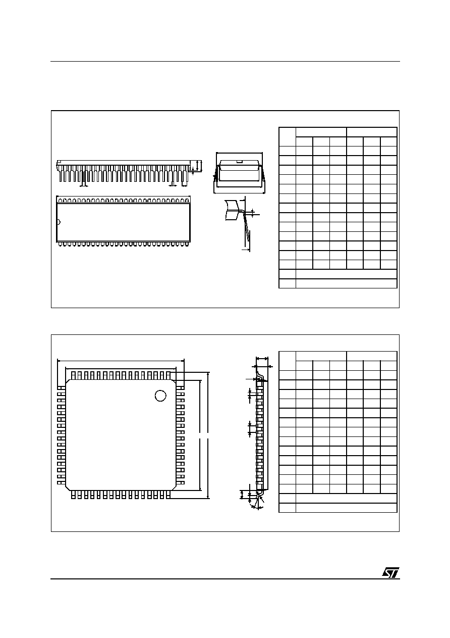
224/230
ST92163 - GENERAL INFORMATION
10.2 PACKAGE DESCRIPTION
Figure 92. 56-Pin Plastic Dual In-Line Package, Shrink 600-mil Width
Figure 93. 64-Pin Thin Quad Flat Package
Dim.
mm
inches
Min
Typ
Max
Min
Typ
Max
A
6.35
0.250
A1
0.38
0.015
A2
3.18
4.95 0.125
0.195
b
0.41
0.016
b2
0.89
0.035
C
0.20
0.38 0.008
0.015
D
50.29
53.21 1.980
2.095
E
15.01
0.591
E1
12.32
14.73 0.485
0.580
e
1.78
0.070
eA
15.24
0.600
eB
17.78
0.700
L
2.92
5.08 0.115
0.200
Number of Pins
N
56
E
0.015
GAGE PLANE
eB
eB
eA
E1
E
C
A
A2
A1
e
b
b2
D
E
b
Dim.
mm
inches
Min
Typ
Max
Min
Typ
Max
A
1.60
0.063
A1
0.05
0.15 0.002
0.006
A2
1.35
1.40
1.45 0.053 0.055 0.057
b
0.30
0.37
0.45 0.012 0.015 0.018
c
0.09
0.20 0.004
0.008
D
16.00
0.630
D1
14.00
0.551
E
16.00
0.630
E1
14.00
0.551
e
0.80
0.031
0∞
3.5∞
7∞
0∞
3.5∞
7∞
L
0.45
0.60
0.75 0.018 0.024 0.030
L1
1.00
0.039
Number of Pins
N
64
c
h
L
L1
e
b
A
A1
A2
E
E1
D
D1
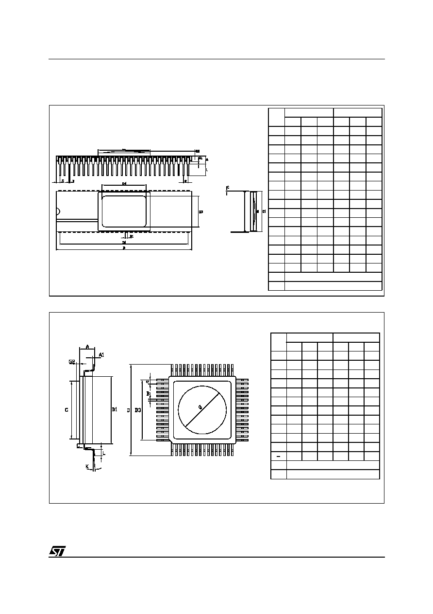
225/230
ST92163 - GENERAL INFORMATION
PACKAGE DESCRIPTION (Cont'd)
Figure 94. 56-Pin Shrink Ceramic Dual In-Line Package, 600-mil Width
Figure 95. 64-Pin Ceramic Quad Flat Package
Dim.
mm
inches
Min
Typ
Max
Min
Typ
Max
A
4.17
0.164
A1
0.76
0.030
B
0.38
0.46
0.56 0.015 0.018 0.022
B1
0.76
0.89
1.02 0.030 0.035 0.040
C
0.23
0.25
0.38 0.009 0.010 0.015
D
50.04 50.80 51.56 1.970 2.000 2.030
D1
48.01
1.890
E1
14.48 14.99 15.49 0.570 0.590 0.610
e
1.78
0.070
G
14.12 14.38 14.63 0.556 0.566 0.576
G1
18.69 18.95 19.20 0.736 0.746 0.756
G2
1.14
0.045
G3
11.05 11.30 11.56 0.435 0.445 0.455
G4
15.11 15.37 15.62 0.595 0.605 0.615
L
2.92
5.08 0.115
0.200
S
1.40
0.055
Number of Pins
N
56
CDIP56SW
Dim
mm
inches
Min
Typ
Max
Min
Typ
Max
A
3.27
0.129
A1
0.50
0.020
B
0.30 0.35 0.45 0.012 0.014 0.018
C
0.13 0.15 0.23 0.005 0.006 0.009
D
16.65 17.20 17.75 0.656 0.677 0.699
D1
13.57 13.97 14.37 0.534 0.550 0.566
D3
12.00
0.472
e
0.80
0.031
G
12.70
0.500
G2
0.96
0.038
L
0.35 0.80
0.014 0.031
0
8.31
0.327
Number of Pins
N
64
CQFP064W
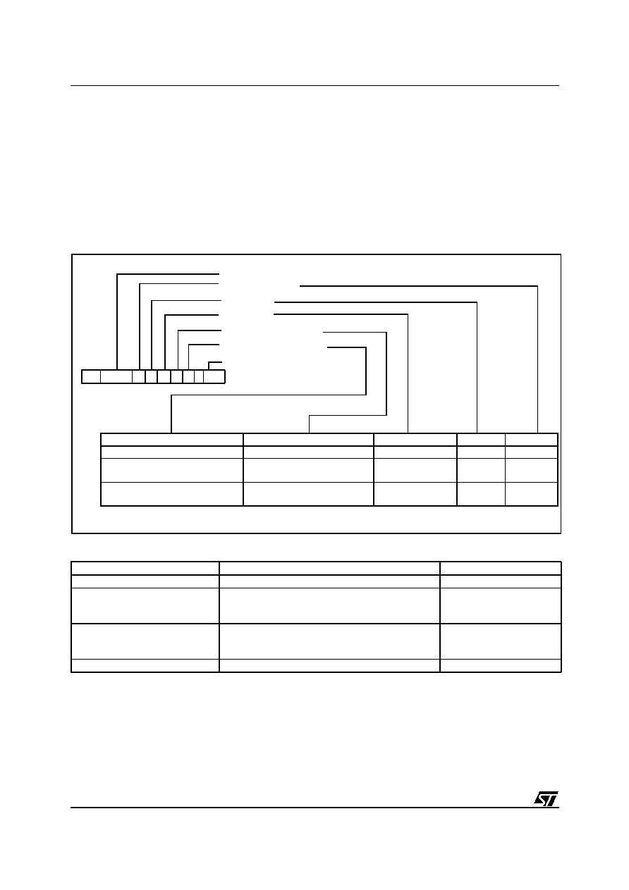
226/230
ST92163 - GENERAL INFORMATION
10.3 ORDERING INFORMATION
The following section deals with the procedure for
transfer of customer codes to STMicroelectronics.
10.4 Transfer of Customer Code
Customer code is made up of the ROM contents.
The ROM contents are to be sent on diskette, or
by electronic means, with the hexadecimal file
generated by the development tool. All unused
bytes must be set to FFh.
The customer code should be communicated to
STMicroelectronics with the correctly completed
OPTION LIST appended.
The STMicroelectronics Sales Organization will be
pleased to provide detailed information on con-
tractual points.
Figure 96. Sales Type Coding Rules
Table 39. Development Tools
Note 1: The emulator does not support Low Voltage Modes
Development Tool
Sales Type
Remarks
Real time emulator
1
ST92163-EMU2
EPROM Programming Board
ST92E163-EPB/EU
ST92E163-EPB/US
220V Power Supply
110V Power Supply
Gang Programmer
ST92E16x-GP/DIP56
ST92E16x-GP/QFP
SDIP56 package
TQFP64 package
C Hiware Compiler and Debugger
ST9P-SWC/V4
for PC
ST 92163 R 4 B 1 L / xxx
Family (92163, 92E163, 92T163)
Number of pins
ROM size
Package
Temperature Range
Device Characteristics
ROM Code (three letters)
L = 8-MHz Low Voltage Version
1= Standard (0 to +70∞C)
B = Plastic DIP
4 = 20K
N = 56 pins
V = 16-MHz Low Voltage Version 0= 25∞C
D = Ceramic DIP
R = 64 pins
E = Without LVD function (for
Normal Voltage Versions)
G = Ceramic QFP
T = Plastic TQFP
No letter = With LVD function (for
Normal Voltage Versions)
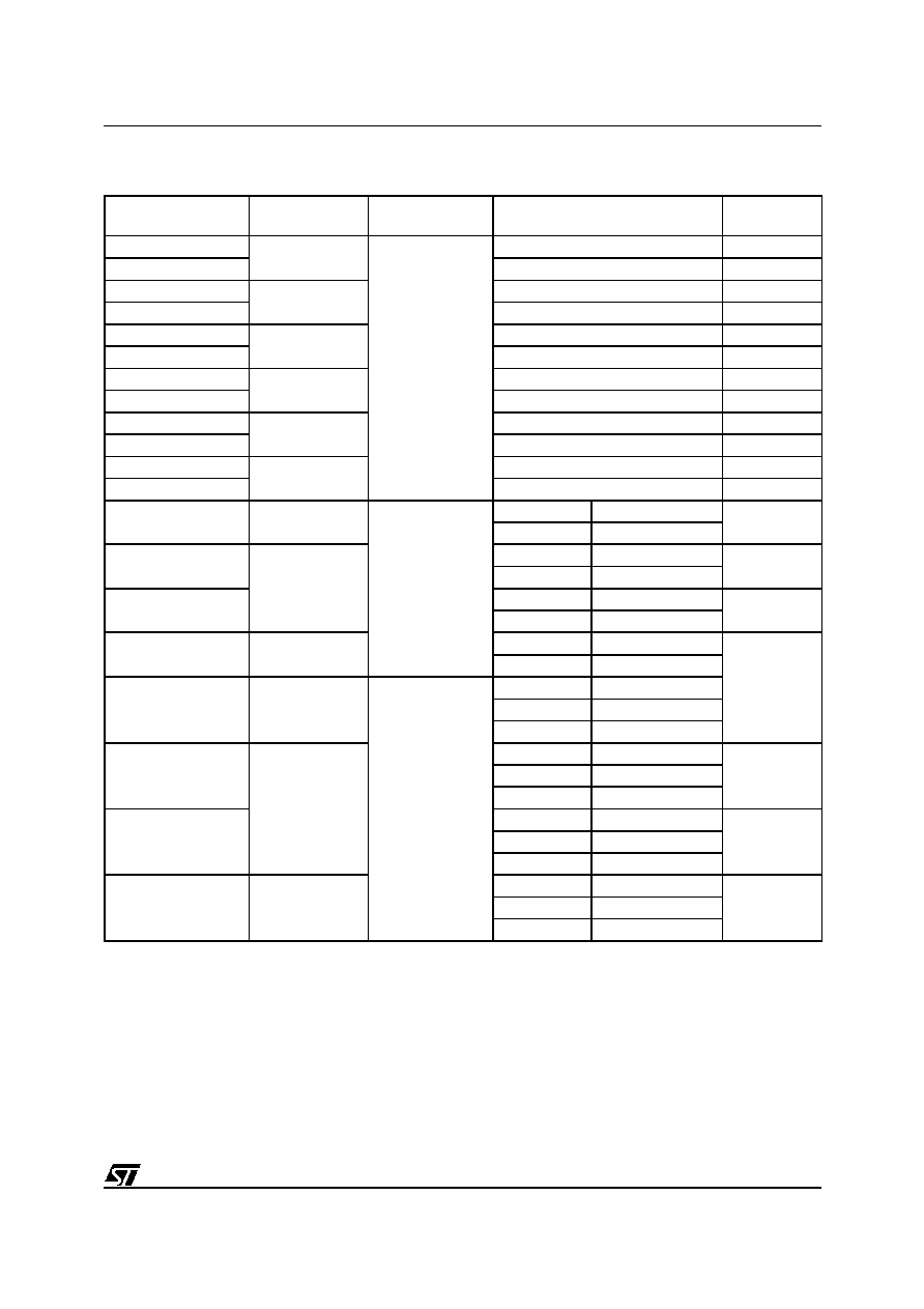
227/230
ST92163 - GENERAL INFORMATION
Table 40. Ordering Information
Note 1: xxx stands for the ROM code name assigned by STMicroelectronics
Note 2: Contact sales office for availability
Note 3: LVM = Low Voltage Mode and NM = Normal Mode
Sales Type
1)
Program Memory
(bytes)
Mode
Operating Voltage
Package
ST92163N4B1/xxx
2)
20K ROM
Normal
4.0-5.5 V
PSDIP56
ST92163R4T1/xxx
2)
4.0-5.5 V
TQFP64
ST92E163N4D0
20K EPROM
4.0-5.5 V
CSDIP56
ST92E163R4G0
4.0-5.5 V
CQFP64
ST92T163N4B1
20K OTP
4.0-5.5 V
PSDIP56
ST92T163R4T1
4.0-5.5 V
TQFP64
ST92163N4B1E/xxx
2)
20K ROM
4.0-5.5 V
PSDIP56
ST92163R4T1E/xxx
2)
4.0-5.5 V
TQFP64
ST92E163N4D1E
20K EPROM
4.0-5.5 V
CSDIP56
ST92E163R4G1E
4.0-5.5 V
CQFP64
ST92T163N4B1E
20K OTP
4.0-5.5 V
PSDIP56
ST92T163R4T1E
4.0-5.5 V
TQFP64
ST92163R4T1L/xxx
2)
20K ROM
Normal
and
8-MHz Low Voltage
8-MHz LVM
3)
3.0-4.0 V (@8Mhz)
TQFP64
NM
3)
4.0-5.5 V
ST92E163R4G1L
20K EPROM
8-MHz LVM
3)
3.0-4.0 V (@8Mhz)
CQFP64
NM
3)
4.0-5.5 V
ST92E163N4D1L
8-MHz LVM
3)
3.0-4.0 V (@8Mhz)
CSDIP56
NM
3)
4.0-5.5 V
ST92T163R4T1L
20K OTP
8-MHz LVM
3)
3.0-4.0 V (@8Mhz)
TQFP64
NM
3)
4.0-5.5 V
ST92163R4T1V/xxx
2)
20K ROM
Normal,
8-MHz Low Voltage
and
16-MHz Low voltage
16-MHz LVM
3)
3.0V-4.0 (@16Mhz)
8-MHz LVM
3)
3.0V-4.0 (@8Mhz)
NM
3)
4.0-5.5V
ST92E163R4T1V
2)
20K EPROM
16-MHz LVM
3)
3.0V-4.0 (@16Mhz)
CQFP64
8-MHz LVM
3)
3.0V-4.0 (@8Mhz)
NM
3)
4.0-5.5V
ST92E163N4D1V
2)
16-MHz LVM
3)
3.0V-4.0 (@16Mhz)
CSDIP56
8-MHz LVM
3)
3.0V-4.0 (@8Mhz)
NM
3)
4.0-5.5V
ST92T163R4T1V
2)
20K OTP
16-MHz LVM
3)
3.0V-4.0 (@16Mhz)
TQFP64
8-MHz LVM
3)
3.0V-4.0 (@8Mhz)
NM
3)
4.0-5.5V

228/230
ST92163 - GENERAL INFORMATION
ST92163 OPTION LIST
Customer: . . . . . . . . . . . . . . . . . . . . . . . . . . . .
Address:
. . . . . . . . . . . . . . . . . . . . . . . . . . . .
. . . . . . . . . . . . . . . . . . . . . . . . . . . .
Contact:
. . . . . . . . . . . . . . . . . . . . . . . . . . . .
Phone No: . . . . . . . . . . . . . . . . . . . . . . . . . . . .
Reference/ROM Code*: . . . . . . . . . . . . . . . . . . .
*The ROM code name is assigned by STMicroelectronics.
STMicroelectronics reference:
Device (TQFP64): [
]
ST92163R4T1/xxx*
[ ] ST92163R4T1E/xxx*
[ ] ST92163R4T1L/xxx*
[ ] ST92163R4T1V/xxx*
Conditioning
[ ] Tray
[ ] Tape and reel
Die form:
[ ] Inked unscribed wafers
[ ] Inked and scribed wafers
*xxx = ROM code name
Software Development:
[ ] STMicroelectronics
[ ] Customer
[ ] External laboratory
ST logo 92163/xxx (line 1)
Special Marking (line 2):
[ ] No
[ ] Yes "_ _ _ _ _ _ _ _ _ _ _ _ _ _ _ _"
For marking, one line is possible with maximum 10 characters for TQFP64
Authorized characters are letters, digits, '.', '-', '/' and spaces only.
Date
. . . . . . . . . . . . . . . . . . . . . . . . . . . .
Signature . . . . . . . . . . . . . . . . . . . . . . . . . . . .

229/230
ST92163 - SUMMARY OF CHANGES
11 SUMMARY OF CHANGES
Revision
Main changes
Date
2.4
SCI synchronous mode max. frequency changed from 3 to 6 MHZ on page 1.
Added higher F
RxCKIN
and F
TxCKIN
max. values with special conditions to SCI timing table
in
Section 9 ELECTRICAL CHARACTERISTICS
.
Jan 02

230/230
ST92163 - SUMMARY OF CHANGES
Notes:
Information furnished is believed to be accurate and reliable. However, STMicroelectronics assumes no responsibility for the consequences
of use of such information nor for any infringement of patents or other rights of third parties which may result from its use. No license is granted
by implication or otherwise under any patent or patent rights of STMicroelectronics. Specifications mentioned in this publication are subject
to change without notice. This publication supersedes and replaces all information previously supplied. STMicroelectronics products are not
authorized for use as critical components in life support devices or systems without the express written approval of STMicroelectronics.
The ST logo is a registered trademark of STMicroelectronics
©
2002 STMicroelectronics - All Rights Reserved.
Purchase of I
2
C Components by STMicroelectronics conveys a license under the Philips I
2
C Patent. Rights to use these components in an
I
2
C system is granted provided that the system conforms to the I
2
C Standard Specification as defined by Philips.
STMicroelectronics Group of Companies
Australia - Brazil - Canada - China - Finland - France - Germany - Hong Kong - India - Israel - Italy - Japan
Malaysia - Malta - Morocco - Singapore - Spain - Sweden - Switzerland - United Kingdom - U.S.A.
http://www.st.com