
September 2002
1/324
Rev. 2.6
ST92F120
8/16-BIT FLASH MCU FAMILY
WITH RAM, EEPROM AND J1850 BLPD
DATASHEET
s
Memories
≠ Internal Memory: up to 128 Kbytes Single
Voltage FLASH, 2 to 4 Kbytes RAM, 1K byte
emulated EEPROM (E3PROM
TM
)
≠ 224 general purpose registers (register file)
available as RAM, accumulators or index
pointers
s
Clock, Reset and Supply Management
≠ Register-oriented 8/16 bit CORE with RUN,
WFI, SLOW, HALT and STOP modes
≠ 0-24 MHz Operation (internal Clock), 4.5 - 5.5
Volt voltage range
≠ PLL Clock Generator (3-5 MHz crystal)
≠ Min. instruction time: 83 ns (24 MHz int.
clock)
s
Interrupt Management
≠ 77 I/O pins
≠ 4 external fast interrupts + 1 NMI
≠ Up to 16 pins programmable as wake-up or
additional external interrupt with multi-level in-
terrupt handler
s
Timers
≠ 16-bit Timer with 8 bit Prescaler, able to be
used as a Watchdog Timer with a large range
of service time (HW/SW enabling through
dedicated pin)
≠ 16-bit Standard Timer that can be used to
generate a time base independent of PLL
Clock Generator
≠ Two 16-bit independent Extended Function
Timers (EFTs) with Prescaler, 2 Input Cap-
tures and two Output Compares
≠ Two 16-bit Multifunction Timers, with Prescal-
er, 2 Input Captures and 2 Output Compares
s
Communication Interfaces
≠ 2 Serial Communication Interfaces with asyn-
chronous and synchronous capabilities. Soft-
ware Management and synchronous mode
supported
≠ Serial Peripheral Interface (SPI) with Selecta-
ble Master/Slave mode
≠ J1850 Byte Level Protocol Decoder (JBLPD)
(on J versions only)
≠ Full I≤C multiple Master/Slave Interface sup-
porting Access Bus
s
8-bit Analog to Digital Converter allowing up
to 16 input channels
s
DMA Controller for reduced processor
overhead
s
Instruction Set
≠ Rich Instruction Set with 14 Addressing
Modes
≠ Division-by-zero trap generation
s
Development Tools
≠ Versatile Development Tools, including As-
sembler, Linker, C-Compiler, Archiver,
Source Level Debugger, Hardware Emulators
and Real Time Operating System
DEVICE SUMMARY
PQFP100
Features
ST92F120V9
ST92F120JV9
ST92F120V1
ST92F120JV1
FLASH - bytes
60K
128K
RAM - bytes
2K
4K
E3PROM - bytes
1K
Network Interface
--
J1850
--
J1850
Temp. Range
-40
o
C to 105
o
C or -40
o
C to 85
o
C
Packages
PQFP100
9

2/324
Table of Contents
324
9
1 GENERAL DESCRIPTION . . . . . . . . . . . . . . . . . . . . . . . . . . . . . . . . . . . . . . . . . . . . . . . . . . . . . . 4
1.1 INTRODUCTION . . . . . . . . . . . . . . . . . . . . . . . . . . . . . . . . . . . . . . . . . . . . . . . . . . . . . . . . . 4
1.2 PIN DESCRIPTION . . . . . . . . . . . . . . . . . . . . . . . . . . . . . . . . . . . . . . . . . . . . . . . . . . . . . . . 6
1.3 I/O PORTS . . . . . . . . . . . . . . . . . . . . . . . . . . . . . . . . . . . . . . . . . . . . . . . . . . . . . . . . . . . . . 14
1.4 OPERATING MODES . . . . . . . . . . . . . . . . . . . . . . . . . . . . . . . . . . . . . . . . . . . . . . . . . . . . 19
2 DEVICE ARCHITECTURE . . . . . . . . . . . . . . . . . . . . . . . . . . . . . . . . . . . . . . . . . . . . . . . . . . . . . 20
2.1 CORE ARCHITECTURE . . . . . . . . . . . . . . . . . . . . . . . . . . . . . . . . . . . . . . . . . . . . . . . . . . 20
2.2 MEMORY SPACES . . . . . . . . . . . . . . . . . . . . . . . . . . . . . . . . . . . . . . . . . . . . . . . . . . . . . . 20
2.3 SYSTEM REGISTERS . . . . . . . . . . . . . . . . . . . . . . . . . . . . . . . . . . . . . . . . . . . . . . . . . . . . 23
2.4 MEMORY ORGANIZATION . . . . . . . . . . . . . . . . . . . . . . . . . . . . . . . . . . . . . . . . . . . . . . . . 31
2.5 MEMORY MANAGEMENT UNIT . . . . . . . . . . . . . . . . . . . . . . . . . . . . . . . . . . . . . . . . . . . . 32
2.6 ADDRESS SPACE EXTENSION . . . . . . . . . . . . . . . . . . . . . . . . . . . . . . . . . . . . . . . . . . . . 33
2.7 MMU REGISTERS . . . . . . . . . . . . . . . . . . . . . . . . . . . . . . . . . . . . . . . . . . . . . . . . . . . . . . . 34
2.8 MMU USAGE . . . . . . . . . . . . . . . . . . . . . . . . . . . . . . . . . . . . . . . . . . . . . . . . . . . . . . . . . . . 38
3 SINGLE VOLTAGE FLASH & EEPROM . . . . . . . . . . . . . . . . . . . . . . . . . . . . . . . . . . . . . . . . . . 39
3.1 INTRODUCTION . . . . . . . . . . . . . . . . . . . . . . . . . . . . . . . . . . . . . . . . . . . . . . . . . . . . . . . . 39
3.2 FUNCTIONAL DESCRIPTION . . . . . . . . . . . . . . . . . . . . . . . . . . . . . . . . . . . . . . . . . . . . . . 40
3.3 REGISTER DESCRIPTION . . . . . . . . . . . . . . . . . . . . . . . . . . . . . . . . . . . . . . . . . . . . . . . . 42
3.4 WRITE OPERATION EXAMPLE . . . . . . . . . . . . . . . . . . . . . . . . . . . . . . . . . . . . . . . . . . . . 47
3.5 EEPROM . . . . . . . . . . . . . . . . . . . . . . . . . . . . . . . . . . . . . . . . . . . . . . . . . . . . . . . . . . . . . . 48
3.6 PROTECTION STRATEGY . . . . . . . . . . . . . . . . . . . . . . . . . . . . . . . . . . . . . . . . . . . . . . . . 50
3.7 FLASH IN-SYSTEM PROGRAMMING . . . . . . . . . . . . . . . . . . . . . . . . . . . . . . . . . . . . . . . 52
4 REGISTER AND MEMORY MAP . . . . . . . . . . . . . . . . . . . . . . . . . . . . . . . . . . . . . . . . . . . . . . . . 54
4.1 INTRODUCTION . . . . . . . . . . . . . . . . . . . . . . . . . . . . . . . . . . . . . . . . . . . . . . . . . . . . . . . . 54
4.2 MEMORY CONFIGURATION . . . . . . . . . . . . . . . . . . . . . . . . . . . . . . . . . . . . . . . . . . . . . . 54
4.3 ST92F120 REGISTER MAP . . . . . . . . . . . . . . . . . . . . . . . . . . . . . . . . . . . . . . . . . . . . . . . 57
5 INTERRUPTS . . . . . . . . . . . . . . . . . . . . . . . . . . . . . . . . . . . . . . . . . . . . . . . . . . . . . . . . . . . . . . . 67
5.1 INTRODUCTION . . . . . . . . . . . . . . . . . . . . . . . . . . . . . . . . . . . . . . . . . . . . . . . . . . . . . . . . 67
5.2 INTERRUPT VECTORING . . . . . . . . . . . . . . . . . . . . . . . . . . . . . . . . . . . . . . . . . . . . . . . . 67
5.3 INTERRUPT PRIORITY LEVELS . . . . . . . . . . . . . . . . . . . . . . . . . . . . . . . . . . . . . . . . . . . 68
5.4 PRIORITY LEVEL ARBITRATION . . . . . . . . . . . . . . . . . . . . . . . . . . . . . . . . . . . . . . . . . . . 68
5.5 ARBITRATION MODES . . . . . . . . . . . . . . . . . . . . . . . . . . . . . . . . . . . . . . . . . . . . . . . . . . . 69
5.6 EXTERNAL INTERRUPTS . . . . . . . . . . . . . . . . . . . . . . . . . . . . . . . . . . . . . . . . . . . . . . . . 74
5.7 TOP LEVEL INTERRUPT . . . . . . . . . . . . . . . . . . . . . . . . . . . . . . . . . . . . . . . . . . . . . . . . . 76
5.8 ON-CHIP PERIPHERAL INTERRUPTS . . . . . . . . . . . . . . . . . . . . . . . . . . . . . . . . . . . . . . 76
5.9 INTERRUPT RESPONSE TIME . . . . . . . . . . . . . . . . . . . . . . . . . . . . . . . . . . . . . . . . . . . . 77
5.10 INTERRUPT REGISTERS . . . . . . . . . . . . . . . . . . . . . . . . . . . . . . . . . . . . . . . . . . . . . . . . . 78
5.11 WAKE-UP / INTERRUPT LINES MANAGEMENT UNIT (WUIMU) . . . . . . . . . . . . . . . . . . 81
6 ON-CHIP DIRECT MEMORY ACCESS (DMA) . . . . . . . . . . . . . . . . . . . . . . . . . . . . . . . . . . . . . . 89
6.1 INTRODUCTION . . . . . . . . . . . . . . . . . . . . . . . . . . . . . . . . . . . . . . . . . . . . . . . . . . . . . . . . 89
6.2 DMA PRIORITY LEVELS . . . . . . . . . . . . . . . . . . . . . . . . . . . . . . . . . . . . . . . . . . . . . . . . . . 89
6.3 DMA TRANSACTIONS . . . . . . . . . . . . . . . . . . . . . . . . . . . . . . . . . . . . . . . . . . . . . . . . . . . 90
6.4 DMA CYCLE TIME . . . . . . . . . . . . . . . . . . . . . . . . . . . . . . . . . . . . . . . . . . . . . . . . . . . . . . . 92
6.5 SWAP MODE . . . . . . . . . . . . . . . . . . . . . . . . . . . . . . . . . . . . . . . . . . . . . . . . . . . . . . . . . . . 92
6.6 DMA REGISTERS . . . . . . . . . . . . . . . . . . . . . . . . . . . . . . . . . . . . . . . . . . . . . . . . . . . . . . . 93
7 RESET AND CLOCK CONTROL UNIT (RCCU) . . . . . . . . . . . . . . . . . . . . . . . . . . . . . . . . . . . . 94

3/324
Table of Contents
9
7.1 INTRODUCTION . . . . . . . . . . . . . . . . . . . . . . . . . . . . . . . . . . . . . . . . . . . . . . . . . . . . . . . . 94
7.2 CLOCK CONTROL UNIT . . . . . . . . . . . . . . . . . . . . . . . . . . . . . . . . . . . . . . . . . . . . . . . . . . 94
7.3 CLOCK MANAGEMENT . . . . . . . . . . . . . . . . . . . . . . . . . . . . . . . . . . . . . . . . . . . . . . . . . . 96
7.4 CLOCK CONTROL REGISTERS . . . . . . . . . . . . . . . . . . . . . . . . . . . . . . . . . . . . . . . . . . . 101
7.5 OSCILLATOR CHARACTERISTICS . . . . . . . . . . . . . . . . . . . . . . . . . . . . . . . . . . . . . . . . 104
7.6 RESET/STOP MANAGER . . . . . . . . . . . . . . . . . . . . . . . . . . . . . . . . . . . . . . . . . . . . . . . . 106
7.7 STOP MODE . . . . . . . . . . . . . . . . . . . . . . . . . . . . . . . . . . . . . . . . . . . . . . . . . . . . . . . . . . 108
8 EXTERNAL MEMORY INTERFACE (EXTMI) . . . . . . . . . . . . . . . . . . . . . . . . . . . . . . . . . . . . . 109
8.1 INTRODUCTION . . . . . . . . . . . . . . . . . . . . . . . . . . . . . . . . . . . . . . . . . . . . . . . . . . . . . . . 109
8.2 EXTERNAL MEMORY SIGNALS . . . . . . . . . . . . . . . . . . . . . . . . . . . . . . . . . . . . . . . . . . . 110
8.3 REGISTER DESCRIPTION . . . . . . . . . . . . . . . . . . . . . . . . . . . . . . . . . . . . . . . . . . . . . . . 115
9 I/O PORTS . . . . . . . . . . . . . . . . . . . . . . . . . . . . . . . . . . . . . . . . . . . . . . . . . . . . . . . . . . . . . . . . . 118
9.1 INTRODUCTION . . . . . . . . . . . . . . . . . . . . . . . . . . . . . . . . . . . . . . . . . . . . . . . . . . . . . . . 118
9.2 SPECIFIC PORT CONFIGURATIONS . . . . . . . . . . . . . . . . . . . . . . . . . . . . . . . . . . . . . . 118
9.3 PORT CONTROL REGISTERS . . . . . . . . . . . . . . . . . . . . . . . . . . . . . . . . . . . . . . . . . . . . 118
9.4 INPUT/OUTPUT BIT CONFIGURATION . . . . . . . . . . . . . . . . . . . . . . . . . . . . . . . . . . . . . 119
9.5 ALTERNATE FUNCTION ARCHITECTURE . . . . . . . . . . . . . . . . . . . . . . . . . . . . . . . . . . 123
9.6 I/O STATUS AFTER WFI, HALT AND RESET . . . . . . . . . . . . . . . . . . . . . . . . . . . . . . . . 123
10 ON-CHIP PERIPHERALS . . . . . . . . . . . . . . . . . . . . . . . . . . . . . . . . . . . . . . . . . . . . . . . . . . . . 124
10.1 TIMER/WATCHDOG (WDT) . . . . . . . . . . . . . . . . . . . . . . . . . . . . . . . . . . . . . . . . . . . . . . 124
10.2 STANDARD TIMER (STIM) . . . . . . . . . . . . . . . . . . . . . . . . . . . . . . . . . . . . . . . . . . . . . . . 131
10.3 EXTENDED FUNCTION TIMER (EFT) . . . . . . . . . . . . . . . . . . . . . . . . . . . . . . . . . . . . . . 135
10.4 MULTIFUNCTION TIMER (MFT) . . . . . . . . . . . . . . . . . . . . . . . . . . . . . . . . . . . . . . . . . . . 155
10.5 MULTIPROTOCOL SERIAL COMMUNICATIONS INTERFACE (SCI-M) . . . . . . . . . . . . 179
10.6 SERIAL PERIPHERAL INTERFACE (SPI) . . . . . . . . . . . . . . . . . . . . . . . . . . . . . . . . . . . 204
10.7 I2C BUS INTERFACE . . . . . . . . . . . . . . . . . . . . . . . . . . . . . . . . . . . . . . . . . . . . . . . . . . . 21 6
10.8 J1850 BYTE LEVEL PROTOCOL DECODER (JBLPD) . . . . . . . . . . . . . . . . . . . . . . . . . 238
10.9 EIGHT-CHANNEL ANALOG TO DIGITAL CONVERTER (A/D) . . . . . . . . . . . . . . . . . . . 279
11 ELECTRICAL CHARACTERISTICS . . . . . . . . . . . . . . . . . . . . . . . . . . . . . . . . . . . . . . . . . . . . 287
12 PACKAGE MECHANICAL DATA . . . . . . . . . . . . . . . . . . . . . . . . . . . . . . . . . . . . . . . . . . . . . . 313
13 DEVICE ORDERING INFORMATION . . . . . . . . . . . . . . . . . . . . . . . . . . . . . . . . . . . . . . . . . . . 314
14 SUMMARY OF CHANGES . . . . . . . . . . . . . . . . . . . . . . . . . . . . . . . . . . . . . . . . . . . . . . . . . . . 315

4/324
ST92F120 - GENERAL DESCRIPTION
1 GENERAL DESCRIPTION
1.1 INTRODUCTION
The ST92F120 microcontroller is developed and
manufactured by STMicroelectronics using a pro-
prietary n-well HCMOS process. Its performance
derives from the use of a flexible 256-register pro-
gramming model for ultra-fast context switching
and real-time event response. The intelligent on-
chip peripherals offload the ST9 core from I/O and
data management processing tasks allowing criti-
cal application tasks to get the maximum use of
core resources. The new-generation ST9 MCU
devices now also support low power consumption
and low voltage operation for power-efficient and
low-cost embedded systems.
1.1.1 ST9+ Core
The advanced Core consists of the Central
Processing Unit (CPU), the Register File, the Inter-
rupt and DMA controller, and the Memory Man-
agement Unit. The MMU allows a single linear ad-
dress space of up to 4 Mbytes.
Four independent buses are controlled by the
Core: a 16-bit memory bus, an 8-bit register data
bus, an 8-bit register address bus and a 6-bit inter-
rupt/DMA bus which connects the interrupt and
DMA controllers in the on-chip peripherals with the
core.
This multiple bus architecture makes the ST9 fam-
ily devices highly efficient for accessing on and off-
chip memory and fast exchange of data with the
on-chip peripherals.
The general-purpose registers can be used as ac-
cumulators, index registers, or address pointers.
Adjacent register pairs make up 16-bit registers for
addressing or 16-bit processing. Although the ST9
has an 8-bit ALU, the chip handles 16-bit opera-
tions, including arithmetic, loads/stores, and mem-
ory/register and memory/memory exchanges.
The powerful I/O capabilities demanded by micro-
controller applications are fulfilled by the
ST92F120 with 77 I/O lines dedicated to digital In-
put/Output. These lines are grouped into up to ten
8-bit I/O Ports and can be configured on a bit basis
under software control to provide timing, status
signals, an address/data bus for interfacing to the
external memory, timer inputs and outputs, analog
inputs, external interrupts and serial or parallel I/O.
Two memory spaces are available to support this
wide range of configurations: a combined Pro-
gram/Data Memory Space and the internal Regis-
ter File, which includes the control and status reg-
isters of the on-chip peripherals.
1.1.2 External Memory Interface
100-pin devices have a 16-bit external address
bus allowing them to address up to 64K bytes of
external memory.
1.1.3 Flash and E3PROM Memories
In the ST92F120, the embedded Flash memory
cell is used to implement emulated EEPROM ca-
pability for applications that require regular up-
dates of single-byte parameters.
1.1.4 On-chip Peripherals
Two 16-bit MultiFunction Timers, each with an 8
bit Prescaler and 12 operating modes allow simple
use for complex waveform generation and meas-
urement, PWM functions and many other system
timing functions by the usage of the two associat-
ed DMA channels for each timer.
Two Extended Function Timers provide further
timing and signal generation capabilities.
A Standard Timer can be used to generate a sta-
ble time base independent from the PLL.
An I
2
C interface provides fast I
2
C and Access Bus
support.
The SPI is a synchronous serial interface for Mas-
ter and Slave device communication. It supports
single master and multimaster systems.
A J1850 Byte Level Protocol Decoder is available
(on some devices only) for communicating with a
J1850 network.
In addition, there is an 16 channel Analog to Digital
Converters with integral sample and hold, fast
conversion time and 8-bit resolution.
Completing the device are two or one full duplex
Serial Communications Interfaces with an integral
generator, asynchronous and synchronous capa-
bility (fully programmable format) and associated
address/wake-up option, plus two DMA channels.
Finally, a programmable PLL Clock Generator al-
lows the usage of standard 3 to 5 MHz crystals to
obtain a large range of internal frequencies up to
24MHz. Low power Run (SLOW), Wait For Inter-
rupt, low power Wait For Interrupt, STOP and
HALT modes are also available.
9
5/324
ST92F120 - GENERAL DESCRIPTION
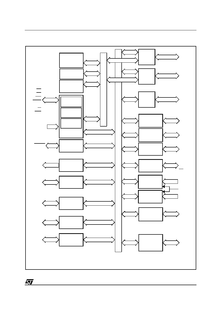
Figure 1. ST92F120JV: Architectural Block Diagram
256 bytes
Register File
ST9 CORE
8/16 bit
CPU
Interrupt
Management
MEMO
RY B
U
S
RCCU
R
EGIS
TER
BUS
WATCHDOG
AS
DS
RW
WAIT
NMI
RW
DS2
MISO
MOSI
SCK
SS
EF TIMER 0
ST. TIMER
SPI
SCI 0
TXCLK0
RXCLK0
SIN0
DCD0
SOUT0
CLKOUT0
RTS0
WDOUT
HW0SW1
WDIN
STOUT
ICAPA0
OCMPA0
ICAPB0
OCMPB0
EXTCLK0
Fully
Prog.
I/Os
P0[7:0]
P1[7:0]
P2[7:0]
P3[7:1]
P4[7:0]
P5[7:0]
P6[5:0]
P7[7:0]
P8[7:0]
P9[7:0]
TXCLK1
RXCLK1
SIN1
DCD1
SOUT1
CLKOUT1
RTS1
MF TIMER 0
TINPA0
TOUTA0
TINPB0
TOUTB0
ICAPA1
OCMPA1
ICAPB1
OCMPB1
EXTCLK1
TINPA1
TOUTA1
TINPB1
TOUTB1
INT[6:0]
WKUP[15:0]
EF TIMER 1
MF TIMER 1
SCI 1
*
OSCIN
OSCOUT
RESET
CLOCK2/8
CLOCK2
INTCLK
A/D CONV. 0
A0IN[7:0]
EXTRG
A/D CONV. 1
A1IN[7:0]
SDAI
SDAO
SCLI
SCLO
I
2
C BUS
VPWI
VPWO
J1850
JBLPD
A[7:0]
D[7:0]
A[15:8]
Ext. MEM.
ADDRESS
DATA
Port0
Ext. MEM.
ADDRESS
Port1
RAM
2/4 Kbytes
FLASH
60/128 Kbytes
EEPROM
1K byte
(optional)
All alternate functions (
Italic characters
) are mapped on Port2, Port3, Port4, Port5, Port6, Port7, Port8 and Port9
* Available on some versions only
9