December 2002
1/398
This is preliminary information on a new product now in development or undergoing evaluation. Details are subject to change without notice.
Rev. 1.3
ST92F124/ST92F150/ST92F250
8/16-BIT SINGLE VOLTAGE FLASH MCU FAMILY WITH RAM,
E
3
TM
(EMULATED EEPROM), CAN 2.0B AND J1850 BLPD
PRELIMINARY DATA
s
Memories
≠ Internal Memory: Single Voltage FLASH up to 256
Kbytes, RAM up to 8Kbytes, 1K byte E
3 TM
(Emulat-
ed EEPROM)
≠ In-Application Programming (IAP)
≠ 224 general purpose registers (register file) availa-
ble as RAM, accumulators or index pointers
s
Clock, Reset and Supply Management
≠ Register-oriented 8/16 bit CORE with RUN, WFI,
SLOW, HALT and STOP modes
≠ 0-24 MHz Operation (Int. Clock), 4.5-5.5 V range
≠ PLL Clock Generator (3-5 MHz crystal)
≠ Minimum instruction time: 83 ns (24 MHz int. clock)
s
80, 77 or 48 I/O pins (depending on device)
s
Interrupt Management
≠ 80, 77 or 48 I/O pins (depending on device)
≠ 4 external fast interrupts + 1 NMI
≠ Up to 16 pins programmable as wake-up or addition-
al external interrupt with multi-level interrupt handler
≠ DMA controller for reduced processor overhead
s
Timers
≠ 16-bit Timer with 8-bit Prescaler, and Watchdog Tim-
er (activated by software or by hardware)
≠ 16-bit Standard Timer that can be used to generate
a time base independent of PLL Clock Generator
≠ Two 16-bit independent Extended Function Timers
(EFTs) with Prescaler, 2 Input Captures and two
Output Compares (100-pin devices only)
≠ Two 16-bit Multifunction Timers, with Prescaler, 2 In-
put Captures and two Output Compares
s
Communication Interfaces
≠ Serial Peripheral Interface (SPI) with Selectable
Master/Slave mode
≠ One Multiprotocol Serial Communications Interface
with asynchronous and synchronous capabilities
≠ One asynchronous Serial Communications Interface
(on 100-pin versions only) with 13-bit LIN Synch
Break generation capability
≠ J1850 Byte Level Protocol Decoder (JBLPD)
(on F150J versions only)
≠ One or two full I≤C multiple Master/Slave Interfaces
supporting Access Bus
≠ One or two CAN 2.0B (150 version only) Active inter-
faces
s
10-bit Analog to Digital Converter allowing up to 16
input channels on 100-pin devices or 8 input channels
on 64-pin devices
s
Development Tools
≠ Free High performance Development environment
(IDE) based on Visual Debugger, Assembler, Linker,
and C-Compiler; Real Time Operating System (OS-
EK OS, CMX) and CAN drivers
≠ Hardware Emulator and Flash Programming Board
for development and ISP Flasher for production
DEVICE SUMMARY
1) see
Section 12.3 on page 396
for important information
2) see
Table 70 on page 393
PQFP100
14x20
TQFP64
14x14
TQFP100
14x14
Features
ST92F124R9
ST92F124V1
ST92F150C(R/V)1
ST92F150JDV1
ST92F250CV2
FLASH - bytes
64K
128K
128K
128K
256K
RAM - bytes
2K
4K
4K
6K
8K
E
3 TM
- bytes
1K
1K
1K
1K
1K
Timers and Serial
Interface
2 MFT, STIM,
WD, SCI, SPI,
I≤C
2 MFT, 2 EFT,
STIM, WD,
2 SCI, SPI, I≤C
2 MFT, 0/2 EFT,
STIM, WD,
1/2 SCI, SPI, I≤C
2 MFT, 2 EFT,
STIM, WD,
2 SCI, SPI, I≤C
2 MFT, 2 EFT, STIM,
WD, 2 SCI,
SPI, 2 I≤C
1)
ADC
8 x 10 bits
16 x 10 bits
8/16 x 10 bits
16 x 10 bits
Network Interface
-
CAN
2 CAN, J1850
CAN, LIN Master
Temp. Range
-40∞C to 85∞C
-40∞C to 105∞C
-40∞C to 105∞C ,
-40∞C to 125∞C
2)
-40
o
C to 125
o
C
-40∞C to 105∞C ,
-40∞C to 125∞C
2)
Packages
TQFP64
PQFP100
P/TQFP100 and
TQFP64
P/TQFP100
9

2/398
Table of Contents
398
9
1 GENERAL DESCRIPTION . . . . . . . . . . . . . . . . . . . . . . . . . . . . . . . . . . . . . . . . . . . . . . . . . . . . . . 4
1.1
INTRODUCTION . . . . . . . . . . . . . . . . . . . . . . . . . . . . . . . . . . . . . . . . . . . . . . . . . . . . . . . . 4
1.2
PIN DESCRIPTION . . . . . . . . . . . . . . . . . . . . . . . . . . . . . . . . . . . . . . . . . . . . . . . . . . . . . 10
1.3
VOLTAGE REGULATOR . . . . . . . . . . . . . . . . . . . . . . . . . . . . . . . . . . . . . . . . . . . . . . . . 22
1.4
I/O PORTS . . . . . . . . . . . . . . . . . . . . . . . . . . . . . . . . . . . . . . . . . . . . . . . . . . . . . . . . . . . . 23
1.5
ALTERNATE FUNCTIONS FOR I/O PORTS . . . . . . . . . . . . . . . . . . . . . . . . . . . . . . . . . 25
1.6
OPERATING MODES . . . . . . . . . . . . . . . . . . . . . . . . . . . . . . . . . . . . . . . . . . . . . . . . . . . 29
2 DEVICE ARCHITECTURE . . . . . . . . . . . . . . . . . . . . . . . . . . . . . . . . . . . . . . . . . . . . . . . . . . . . . 30
2.1
CORE ARCHITECTURE . . . . . . . . . . . . . . . . . . . . . . . . . . . . . . . . . . . . . . . . . . . . . . . . . 30
2.2
MEMORY SPACES . . . . . . . . . . . . . . . . . . . . . . . . . . . . . . . . . . . . . . . . . . . . . . . . . . . . . 30
2.3
SYSTEM REGISTERS . . . . . . . . . . . . . . . . . . . . . . . . . . . . . . . . . . . . . . . . . . . . . . . . . . 33
2.4
MEMORY ORGANIZATION . . . . . . . . . . . . . . . . . . . . . . . . . . . . . . . . . . . . . . . . . . . . . . 41
2.5
MEMORY MANAGEMENT UNIT . . . . . . . . . . . . . . . . . . . . . . . . . . . . . . . . . . . . . . . . . . 42
2.6
ADDRESS SPACE EXTENSION . . . . . . . . . . . . . . . . . . . . . . . . . . . . . . . . . . . . . . . . . . 43
2.7
MMU REGISTERS . . . . . . . . . . . . . . . . . . . . . . . . . . . . . . . . . . . . . . . . . . . . . . . . . . . . . 44
2.8
MMU USAGE . . . . . . . . . . . . . . . . . . . . . . . . . . . . . . . . . . . . . . . . . . . . . . . . . . . . . . . . . . 48
3 SINGLE VOLTAGE FLASH & E3 TM (EMULATED EEPROM) . . . . . . . . . . . . . . . . . . . . . . . . . 49
3.1
INTRODUCTION . . . . . . . . . . . . . . . . . . . . . . . . . . . . . . . . . . . . . . . . . . . . . . . . . . . . . . . 49
3.2
FUNCTIONAL DESCRIPTION . . . . . . . . . . . . . . . . . . . . . . . . . . . . . . . . . . . . . . . . . . . . 51
3.3
REGISTER DESCRIPTION . . . . . . . . . . . . . . . . . . . . . . . . . . . . . . . . . . . . . . . . . . . . . . . 55
3.4
WRITE OPERATION EXAMPLE . . . . . . . . . . . . . . . . . . . . . . . . . . . . . . . . . . . . . . . . . . . 59
3.5
PROTECTION STRATEGY . . . . . . . . . . . . . . . . . . . . . . . . . . . . . . . . . . . . . . . . . . . . . . . 60
3.6
FLASH IN-SYSTEM PROGRAMMING . . . . . . . . . . . . . . . . . . . . . . . . . . . . . . . . . . . . . . 63
4 REGISTER AND MEMORY MAP . . . . . . . . . . . . . . . . . . . . . . . . . . . . . . . . . . . . . . . . . . . . . . . . 65
4.1
INTRODUCTION . . . . . . . . . . . . . . . . . . . . . . . . . . . . . . . . . . . . . . . . . . . . . . . . . . . . . . . 65
4.2
MEMORY CONFIGURATION . . . . . . . . . . . . . . . . . . . . . . . . . . . . . . . . . . . . . . . . . . . . . 65
4.3
ST92F124/F150/F250 REGISTER MAP . . . . . . . . . . . . . . . . . . . . . . . . . . . . . . . . . . . . . 70
5 INTERRUPTS . . . . . . . . . . . . . . . . . . . . . . . . . . . . . . . . . . . . . . . . . . . . . . . . . . . . . . . . . . . . . . . 88
5.1
INTRODUCTION . . . . . . . . . . . . . . . . . . . . . . . . . . . . . . . . . . . . . . . . . . . . . . . . . . . . . . . 88
5.2
INTERRUPT VECTORING . . . . . . . . . . . . . . . . . . . . . . . . . . . . . . . . . . . . . . . . . . . . . . . 88
5.3
INTERRUPT PRIORITY LEVELS . . . . . . . . . . . . . . . . . . . . . . . . . . . . . . . . . . . . . . . . . . 90
5.4
PRIORITY LEVEL ARBITRATION . . . . . . . . . . . . . . . . . . . . . . . . . . . . . . . . . . . . . . . . . 90
5.5
ARBITRATION MODES . . . . . . . . . . . . . . . . . . . . . . . . . . . . . . . . . . . . . . . . . . . . . . . . . 91
5.6
EXTERNAL INTERRUPTS . . . . . . . . . . . . . . . . . . . . . . . . . . . . . . . . . . . . . . . . . . . . . . . 96
5.7
STANDARD INTERRUPTS (CAN AND SCI-A) . . . . . . . . . . . . . . . . . . . . . . . . . . . . . . . . 98
5.8
TOP LEVEL INTERRUPT . . . . . . . . . . . . . . . . . . . . . . . . . . . . . . . . . . . . . . . . . . . . . . . 100
5.9
DEDICATED ON-CHIP PERIPHERAL INTERRUPTS . . . . . . . . . . . . . . . . . . . . . . . . . 100
5.10 INTERRUPT RESPONSE TIME . . . . . . . . . . . . . . . . . . . . . . . . . . . . . . . . . . . . . . . . . . 101
5.11 INTERRUPT REGISTERS . . . . . . . . . . . . . . . . . . . . . . . . . . . . . . . . . . . . . . . . . . . . . . 102
5.12 WAKE-UP / INTERRUPT LINES MANAGEMENT UNIT (WUIMU) . . . . . . . . . . . . . . . . 109
6 ON-CHIP DIRECT MEMORY ACCESS (DMA) . . . . . . . . . . . . . . . . . . . . . . . . . . . . . . . . . . . . . 117
6.1
INTRODUCTION . . . . . . . . . . . . . . . . . . . . . . . . . . . . . . . . . . . . . . . . . . . . . . . . . . . . . . 117
6.2
DMA PRIORITY LEVELS . . . . . . . . . . . . . . . . . . . . . . . . . . . . . . . . . . . . . . . . . . . . . . . 117
6.3
DMA TRANSACTIONS . . . . . . . . . . . . . . . . . . . . . . . . . . . . . . . . . . . . . . . . . . . . . . . . . 118
6.4
DMA CYCLE TIME . . . . . . . . . . . . . . . . . . . . . . . . . . . . . . . . . . . . . . . . . . . . . . . . . . . . 120
6.5
SWAP MODE . . . . . . . . . . . . . . . . . . . . . . . . . . . . . . . . . . . . . . . . . . . . . . . . . . . . . . . . 1 20

3/398
Table of Contents
9
6.6
DMA REGISTERS . . . . . . . . . . . . . . . . . . . . . . . . . . . . . . . . . . . . . . . . . . . . . . . . . . . . . 121
7 RESET AND CLOCK CONTROL UNIT (RCCU) . . . . . . . . . . . . . . . . . . . . . . . . . . . . . . . . . . . . 122
7.1
INTRODUCTION . . . . . . . . . . . . . . . . . . . . . . . . . . . . . . . . . . . . . . . . . . . . . . . . . . . . . . 122
7.2
CLOCK CONTROL UNIT . . . . . . . . . . . . . . . . . . . . . . . . . . . . . . . . . . . . . . . . . . . . . . . . 122
7.3
CLOCK MANAGEMENT . . . . . . . . . . . . . . . . . . . . . . . . . . . . . . . . . . . . . . . . . . . . . . . . 124
7.4
CLOCK CONTROL REGISTERS . . . . . . . . . . . . . . . . . . . . . . . . . . . . . . . . . . . . . . . . . . 130
7.5
CRYSTAL OSCILLATOR . . . . . . . . . . . . . . . . . . . . . . . . . . . . . . . . . . . . . . . . . . . . . . . . 134
7.6
RESET/STOP MANAGER . . . . . . . . . . . . . . . . . . . . . . . . . . . . . . . . . . . . . . . . . . . . . . . 136
8 EXTERNAL MEMORY INTERFACE (EXTMI) . . . . . . . . . . . . . . . . . . . . . . . . . . . . . . . . . . . . . . 138
8.1
INTRODUCTION . . . . . . . . . . . . . . . . . . . . . . . . . . . . . . . . . . . . . . . . . . . . . . . . . . . . . . 138
8.2
EXTERNAL MEMORY SIGNALS . . . . . . . . . . . . . . . . . . . . . . . . . . . . . . . . . . . . . . . . . . 139
8.3
REGISTER DESCRIPTION . . . . . . . . . . . . . . . . . . . . . . . . . . . . . . . . . . . . . . . . . . . . . . 144
9 I/O PORTS . . . . . . . . . . . . . . . . . . . . . . . . . . . . . . . . . . . . . . . . . . . . . . . . . . . . . . . . . . . . . . . . . 147
9.1
INTRODUCTION . . . . . . . . . . . . . . . . . . . . . . . . . . . . . . . . . . . . . . . . . . . . . . . . . . . . . . 147
9.2
SPECIFIC PORT CONFIGURATIONS . . . . . . . . . . . . . . . . . . . . . . . . . . . . . . . . . . . . . 147
9.3
PORT CONTROL REGISTERS . . . . . . . . . . . . . . . . . . . . . . . . . . . . . . . . . . . . . . . . . . . 147
9.4
INPUT/OUTPUT BIT CONFIGURATION . . . . . . . . . . . . . . . . . . . . . . . . . . . . . . . . . . . . 148
9.5
ALTERNATE FUNCTION ARCHITECTURE . . . . . . . . . . . . . . . . . . . . . . . . . . . . . . . . . 152
9.6
I/O STATUS AFTER WFI, HALT AND RESET . . . . . . . . . . . . . . . . . . . . . . . . . . . . . . . 152
10 ON-CHIP PERIPHERALS . . . . . . . . . . . . . . . . . . . . . . . . . . . . . . . . . . . . . . . . . . . . . . . . . . . . 153
10.1 TIMER/WATCHDOG (WDT) . . . . . . . . . . . . . . . . . . . . . . . . . . . . . . . . . . . . . . . . . . . . . 153
10.2 STANDARD TIMER (STIM) . . . . . . . . . . . . . . . . . . . . . . . . . . . . . . . . . . . . . . . . . . . . . . 160
10.3 EXTENDED FUNCTION TIMER (EFT) . . . . . . . . . . . . . . . . . . . . . . . . . . . . . . . . . . . . . 164
10.4 MULTIFUNCTION TIMER (MFT) . . . . . . . . . . . . . . . . . . . . . . . . . . . . . . . . . . . . . . . . . . 185
10.5 MULTIPROTOCOL SERIAL COMMUNICATIONS INTERFACE (SCI-M) . . . . . . . . . . . 209
10.6 ASYNCHRONOUS SERIAL COMMUNICATIONS INTERFACE (SCI-A) . . . . . . . . . . . 234
10.7 SERIAL PERIPHERAL INTERFACE (SPI) . . . . . . . . . . . . . . . . . . . . . . . . . . . . . . . . . . 247
10.8 I2C BUS INTERFACE . . . . . . . . . . . . . . . . . . . . . . . . . . . . . . . . . . . . . . . . . . . . . . . . . . 259
10.9 J1850 BYTE LEVEL PROTOCOL DECODER (JBLPD) . . . . . . . . . . . . . . . . . . . . . . . . 281
10.10 CONTROLLER AREA NETWORK (BXCAN) . . . . . . . . . . . . . . . . . . . . . . . . . . . . . . . . . 322
10.11 10-BIT ANALOG TO DIGITAL CONVERTER (ADC) . . . . . . . . . . . . . . . . . . . . . . . . . . . 358
11 ELECTRICAL CHARACTERISTICS . . . . . . . . . . . . . . . . . . . . . . . . . . . . . . . . . . . . . . . . . . . . 371
12 GENERAL INFORMATION . . . . . . . . . . . . . . . . . . . . . . . . . . . . . . . . . . . . . . . . . . . . . . . . . . . 392
12.1 ORDERING INFORMATION . . . . . . . . . . . . . . . . . . . . . . . . . . . . . . . . . . . . . . . . . . . . . 392
12.2 PACKAGE MECHANICAL DATA . . . . . . . . . . . . . . . . . . . . . . . . . . . . . . . . . . . . . . . . . . 394
12.3 DEVELOPMENT TOOLS . . . . . . . . . . . . . . . . . . . . . . . . . . . . . . . . . . . . . . . . . . . . . . . . 396
13 SUMMARY OF CHANGES . . . . . . . . . . . . . . . . . . . . . . . . . . . . . . . . . . . . . . . . . . . . . . . . . . . 397

4/398
ST92F124/F150/F250 - GENERAL DESCRIPTION
1 GENERAL DESCRIPTION
1.1 INTRODUCTION
The ST92F124/F150/F250 microcontroller is de-
veloped and manufactured by STMicroelectronics
using a proprietary n-well HCMOS process. Its
performance derives from the use of a flexible
256-register programming model for ultra-fast con-
text switching and real-time event response. The
intelligent on-chip peripherals offload the ST9 core
from I/O and data management processing tasks
allowing critical application tasks to get the maxi-
mum use of core resources. The new-generation
ST9 MCU devices now also support low power
consumption and low voltage operation for power-
efficient and low-cost embedded systems.
1.1.1 ST9+ Core
The advanced Core consists of the Central
Processing Unit (CPU), the Register File, the Inter-
rupt and DMA controller, and the Memory Man-
agement Unit. The MMU allows a single linear ad-
dress space of up to 4 Mbytes.
Four independent buses are controlled by the
Core: a 22-bit memory bus, an 8-bit register data
bus, an 8-bit register address bus and a 6-bit inter-
rupt/DMA bus which connects the interrupt and
DMA controllers in the on-chip peripherals with the
core.
This multiple bus architecture makes the ST9 fam-
ily devices highly efficient for accessing on and off-
chip memory and fast exchange of data with the
on-chip peripherals.
The general-purpose registers can be used as ac-
cumulators, index registers, or address pointers.
Adjacent register pairs make up 16-bit registers for
addressing or 16-bit processing. Although the ST9
has an 8-bit ALU, the chip handles 16-bit opera-
tions, including arithmetic, loads/stores, and mem-
ory/register and memory/memory exchanges.
The powerful I/O capabilities demanded by micro-
controller applications are fulfilled by the
ST92F150/F124 with 48 (64-pin devices) or 77
(100-pin devices) I/O lines dedicated to digital In-
put/Output and with 80 I/O lines by the ST92F250.
These lines are grouped into up to ten 8-bit I/O
Ports and can be configured on a bit basis under
software control to provide timing, status signals,
an address/data bus for interfacing to the external
memory, timer inputs and outputs, analog inputs,
external interrupts and serial or parallel I/O. Two
memory spaces are available to support this wide
range of configurations: a combined Program/
Data Memory Space and the internal Register File,
which includes the control and status registers of
the on-chip peripherals.
1.1.2 External Memory Interface
100-pin devices have a 22-bit external address
bus allowing them to address up to 4M bytes of ex-
ternal memory. 64-pin devices have an 11-bit ex-
ternal address bus for addressing up to 2K bytes.
1.1.3 On-chip Peripherals
Two 16-bit Multifunction Timers, each with an 8 bit
Prescaler and 12 operating modes allow simple
use for complex waveform generation and meas-
urement, PWM functions and many other system
timing functions by the usage of the two associat-
ed DMA channels for each timer.
On 100-pin devices, two Extended Function Tim-
ers provide further timing and signal generation
capabilities.
A Standard Timer can be used to generate a sta-
ble time base independent from the PLL.
An I
2
C interface (two in the ST92F250) provides
fast I
2
C and Access Bus support.
The SPI is a synchronous serial interface for Mas-
ter and Slave device communication. It supports
single master and multimaster systems.
A J1850 Byte Level Protocol Decoder is available
(on some devices only) for communicating with a
J1850 network.
The bxCAN (basic extended) interface supports
2.0B Active protocol. It has 3 transmit mailboxes, 2
independent receive FIFOs and 8 filters.
In addition, there is an 16 channel Analog to Digital
Converter with integral sample and hold, fast con-
version time and 10-bit resolution. In the 64-pin
version only 8 input channels are available.
There is one Multiprotocol Serial Communications
Interface with an integral generator, asynchronous
and synchronous capability (fully programmable
format) and associated address/wake-up option,
plus two DMA channels.
On some devices, there is an additional asynchro-
nous Serial Communications interface.
Finally, a programmable PLL Clock Generator al-
lows the usage of standard 3 to 5 MHz crystals to
obtain a large range of internal frequencies up to
24MHz. Low power Run (SLOW), Wait For Inter-
rupt, low power Wait For Interrupt, STOP and
HALT modes are also available.
9
5/398
ST92F124/F150/F250 - GENERAL DESCRIPTION
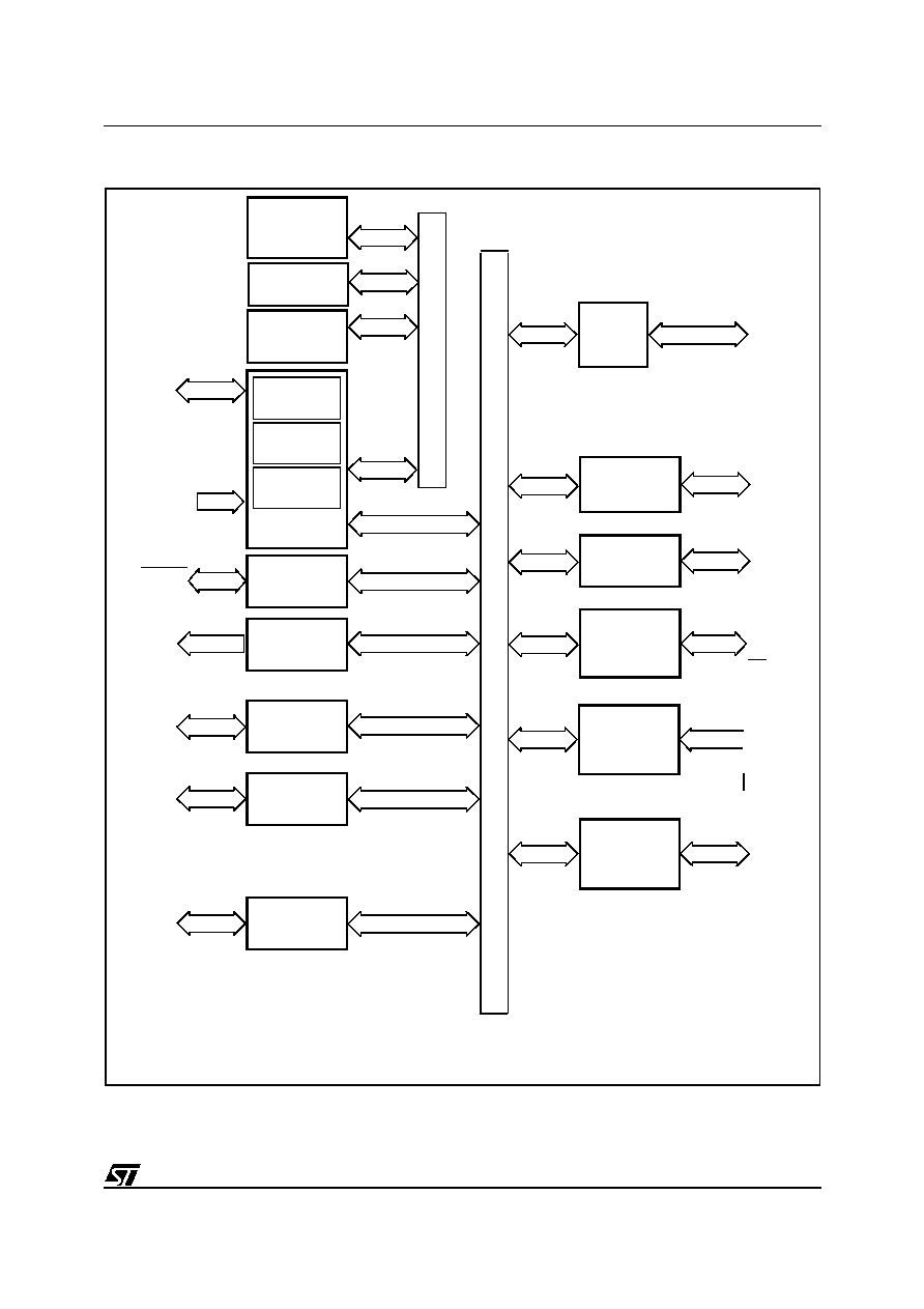
Figure 1. ST92F124R9: Architectural Block Diagram
256 bytes
Register File
RAM
2 Kbytes
ST9 CORE
8/16 bits
CPU
Interrupt
Management
MEMO
RY B
U
S
RCCU
R
EGIS
TER
BUS
WATCHDOG
NMI
MISO
MOSI
SCK
SS
ST. TIMER
SPI
SDA
SCL
I
2
C BUS
SCI M
FLASH
64 Kbytes
TXCLK
RXCLK
SIN
DCD
SOUT
CLKOUT
RTS
WDOUT
HW0SW1
STOUT
Fully
Prog.
I/Os
P0[7:0]
P1[2:0]
P2[7:0]
P3[7:4]
P4[7:4]
P5[7:0]
P6[5:2,0]
P7[7:0]
MF TIMER 0
TINPA0
TOUTA0
TINPB0
TOUTB0
TINPA1
TOUTA1
TINPB1
TOUTB1
INT[5:0]
WKUP[13:0]
MF TIMER 1
E
3 TM
1 Kbyte
OSCIN
OSCOUT
RESET
CLOCK2/8
INTCLK
CK_AF
ADC
AV
DD
AV
SS
AIN[15:8]
EXTRG
V
REG
VOLTAGE
REGULATOR
The alternate functions (
Italic characters
) are mapped on Port 0, Port 1, Port2, Port3, Port4, Port5, Port6
and Port7.
9