ST93CS46
ST93CS47
1K (64 x 16) SERIAL MICROWIRE EEPROM
NOT FOR NEW DESIGN
June 1997
1/16
This is information on a product still in production bu t not recommended for new de signs.
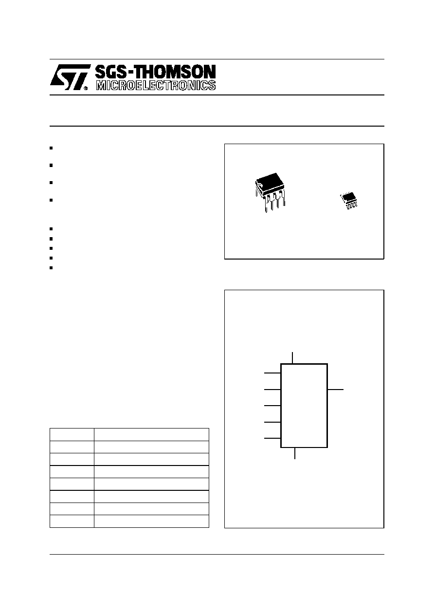
AI00884B
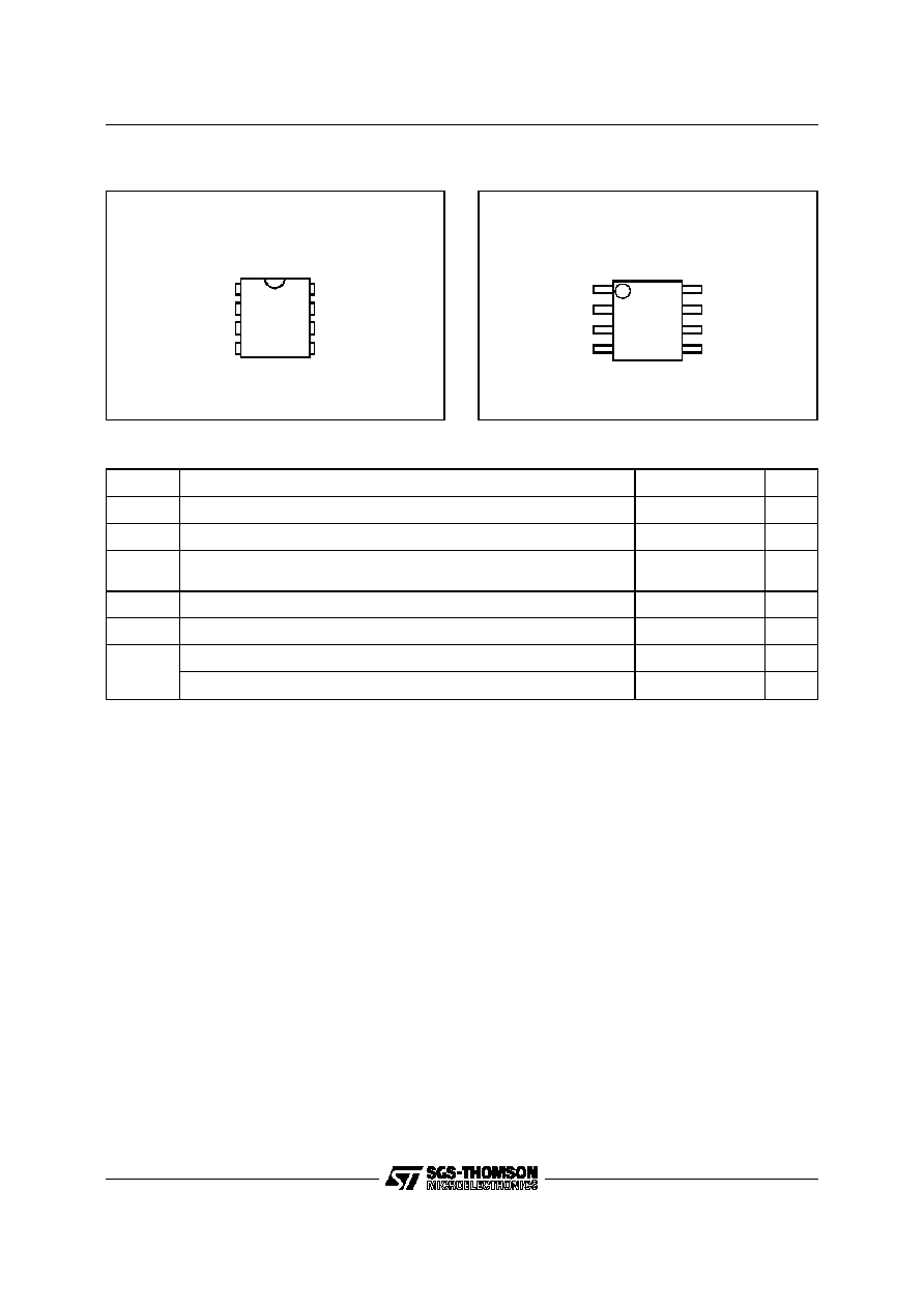
D
VCC
ST93CS46
ST93CS47
VSS
C
Q
PRE
W
S
Figure 1. Logic Diagram
1 MILLION ERASE/WRITE CYCLES, with
40 YEARS DATA RETENTION
SELF-TIMED PROGRAMMING CYCLE with
AUTO-ERASE
READY/BUSY SIGNAL DURING
PROGRAMMING
SINGLE SUPPLY VOLTAGE
≠ 3V to 5.5V for the ST93CS46
≠ 2.5V to 5.5V for the ST93CS47
USER DEFINED WRITE PROTECTED AREA
PAGE WRITE MODE (4 WORDS)
SEQUENTIAL READ OPERATION
5ms TYPICAL PROGRAMMING TIME
ST93CS46 and ST93CS47 are replaced by
the M93S46
DESCRIPTION
The ST93CS46 and ST93CS47 are 1K bit Electri-
cally Erasable Programmable Memory (EEPROM)
fabricated with SGS-THOMSON's High Endurance
Single Polysilicon CMOS technology. The memory
is accessed through a serial input D and output Q.
The 1K bit memory is organized as 64 x 16 bit
words.The memory is accessed by a set of instruc-
tions which include Read, Write, Page Write, Write
All and instructions used to set the memory protec-
tion. A Read instruction loads the address of the
first word to be read into an internal address
pointer.
S
Chip Select Input
D
Serial Data Input
Q
Serial Data Output
C
Serial Clock
PRE
Protect Enable
W
Write Enable
V
CC
Supply Voltage
V
SS
Ground
Table 1. Signal Names
8
1
SO8 (M)
150mil Width
8
1
PSDIP8 (B)
0.4mm Frame
DESCRIPTION (cont'd)
The data is then clocked out serially. The address
pointer is automatically incremented after the data
is output and, if the Chip Select input (S) is held
High, the ST93CS46/47 can output a sequential
stream of data words. In this way, the memory can
be read as a data stream of 16 to 1024 bits, or
continuously as the address counter automatically
rolls over to 00 when the highest address is
reached. Within the time required by a program-
ming cycle (t
W
), up to 4 words may be written with
the help of the Page Write instruction; the whole
memory may also be erased, or set to a predeter-
mined pattern, by using the Write All instruction.
Within the memory, an user defined area may be
protected against further Write instructions. The
size of this area is defined by the content of a
VSS
Q
W
PRE
C
S
VCC
D
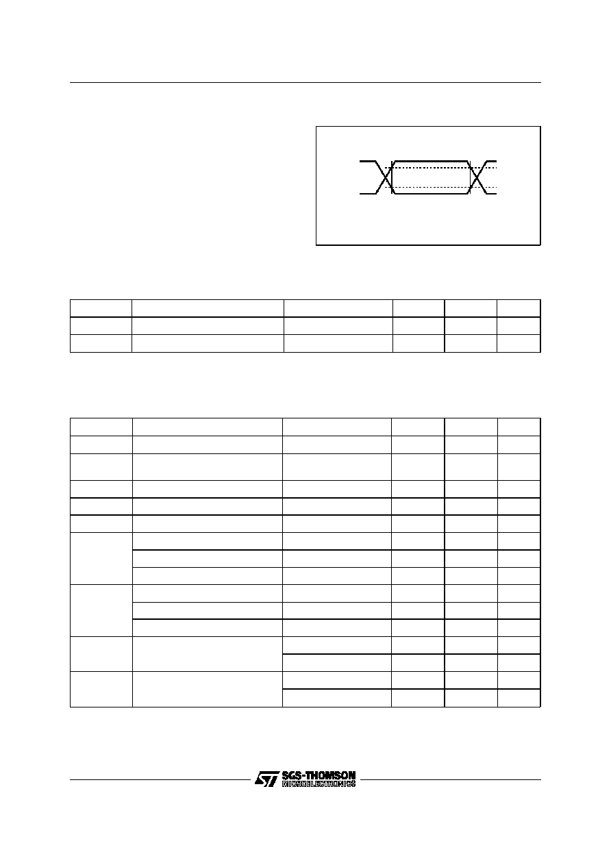
AI00885B
ST93CS46
ST93CS47
1
2
3
4
8
7
6
5
Figure 2A. DIP Pin Connections
1
VSS
Q
W
PRE
C
S
VCC
D
AI00886C
ST93CS46
ST93CS47
2
3
4
8
7
6
5
Figure 2B. SO Pin Connections
Symbol
Parameter
Value
Unit
T
A
Ambient Operating Temperature
≠40 to 85
∞
C
T
STG
Storage Temperature
≠65 to 150
∞
C
T
LEAD
Lead Temperature, Soldering
(SO8 package)
(PSDIP8 package)
40 sec
10 sec
215
260
∞
C
V
IO
Input or Output Voltages (Q = V
OH
or Hi-Z)
≠0.3 to V
CC
+0.5
V
V
CC
Supply Voltage
≠0.3 to 6.5
V
V
ESD
Electrostatic Discharge Voltage (Human Body model)
(2)
3000
V
Electrostatic Discharge Voltage (Machine model)
(3)
500
V
Notes: 1. Except for the rating "Operating Temperature Range", stresses above those listed in the Table "Absolute Maximum Ratings"
may cause permanent damage to the device. These are stress ratings only and operation of the device at these or any other
conditions above those indicated in the Operating sections of this specification is not implied. Exposure to Absolute Maximum
Rating conditions for extended periods may affect device reliability. Refer also to the SGS-THOMSON SURE Program and other
relevant quality documents.
2. MIL-STD-883C, 3015.7 (100pF, 1500
).
3. EIAJ IC-121 (Condition C) (200pF, 0
).
Table 2. Absolute Maximum Ratings
(1)
Protect Register, located outside of the memory
array. As a final protection step, data may be per-
manently protected by programming a One Time
Programing bit (OTP bit) which locks the Protect
Register content.
Programming is internally self-timed (the external
clock signal on C input may be disconnected or left
running after the start of a Write cycle) and does
not require an erase cycle prior to the Write instruc-
tion. The Write instruction writes 16 bits at one time
into one of the 64 words, the Page Write instruction
writes up to 4 words of 16 bits to sequential loca-
tions, assuming in both cases that all addresses
are outside the Write Protected area.
After the start of the programming cycle, a
Ready/Busy signal is available on the Data output
(Q) when the Chip Select (S) input pin is driven
High.
2/16
ST93CS46, ST93CS47
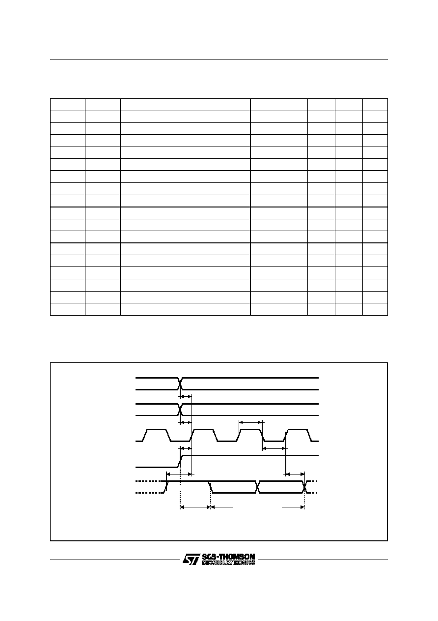
Input Rise and Fall Times
20ns (10% to 90%)
Input Pulse Voltages
0.4V to 2.4V
Input and Output Timing
Reference Voltages
0.8 and 2V
AC MEASUREMENT CONDITIONS
Note that Output Hi-Z is defined as the point where data
is no longer driven.
AI00825
0.8VCC
0.2VCC
0.7VCC
0.3VCC
Figure 3. AC Testing Input Output Waveforms
Symbol
Parameter
Test Condition
Min
Max
Unit
C
IN
Input Capacitance
V
IN
= 0V
5
pF
C
OUT
Output Capacitance
V
OUT
= 0V
5
pF
Note: 1. Sampled only, not 100% tested.
Table 3. Capacitance
(1)
(T
A
= 25
∞
C, f = 1 MHz )
Symbol
Parameter
Test Condition
Min
Max
Unit
I
LI
Input Leakage Current
0V
V
IN
V
CC
±
2.5
µ
A
I
LO
Output Leakage Current
0V
V
OUT
V
CC
,
Q in Hi-Z
±
2.5
µ
A
I
CC
Supply Current (TTL Inputs)
S = V
IH
, f = 1 MHz
3
mA
Supply Current (CMOS Inputs)
S = V
IH
, f = 1 MHz
2
mA
I
CC1
Supply Current (Standby)
S = V
SS
, C = V
SS
50
µ
A
V
IL
Input Low Voltage (ST93CS46,47)
4.5V
V
CC
5.5V
≠0.1
0.8
V
Input Low Voltage (ST93CS46)
3V
V
CC
5.5V
≠0.1
0.2 V
CC
V
Input Low Voltage (ST93CS47)
2.5V
V
CC
5.5V
≠0.1
0.2 V
CC
V
V
IH
Input High Voltage (ST93CS46,47)
4.5V
V
CC
5.5V
2
V
CC
+ 1
V
Input High Voltage (ST93CS46)
3V
V
CC
5.5V
0.8 V
CC
V
CC
+ 1
V
Input High Voltage (ST93CS47)
2.5V
V
CC
5.5V
0.8 V
CC
V
CC
+ 1
V
V
OL
Output Low Voltage
I
OL
= 2.1mA
0.4
V
I
OL
= 10
µ
A
0.2
V
V
OH
Output High Voltage
I
OH
= ≠400
µ
A
2.4
V
I
OH
= ≠10
µ
A
V
CC
≠ 0.2
V
Table 4. DC Characteristics (T
A
= 0 to 70
∞
C or ≠40 to 85
∞
C; V
CC
= 3V to 5.5V for ST93CS46 and
V
CC
= 2.5V to 5.5V for ST93CS47)
3/16
ST93CS46, ST93CS47
Symbol
Alt
Parameter
Test Condition
Min
Max
Unit
t
PRVCH
t
PRES
Protect Enable Valid to Clock High
50
ns
t
WVCH
t
PES
Write Enable Valid to Clock High
50
ns
t
SHCH
t
CSS
Chip Select High to Clock High
50
ns
t
DVCH
t
DIS
Input Valid to Clock High
100
ns
t
CHDX
t
DIH
Clock High to Input Transition
100
ns
t
CHQL
t
PD0
Clock High to Output Low
500
ns
t
CHQV
t
PD1
Clock High to Output Valid
500
ns
t
CLPRX
t
PREH
Clock Low to Protect Enable Transition
0
ns
t
SLWX
t
PEH
Chip Select Low to Write Enable Transition
250
ns
t
CLSL
t
CSH
Clock Low to Chip Select Transition
0
ns
t
SLSH
t
CS
Chip Select Low to Chip Select High
Note 1
250
ns
t
SHQV
t
SV
Chip Select High to Output Valid
500
ns
t
SLQZ
t
DF
Chip Select Low to Output Hi-Z
300
ns
t
CHCL
t
SKH
Clock High to Clock Low
Note 2
250
ns
t
CLCH
t
SKL
Clock Low to Clock High
Note 2
250
ns
t
W
t
WP
Erase/Write Cycle time
10
ms
f
C
f
SK
Clock Frequency
0
1
MHz
Notes: 1. Chip Select must be brought low for a minimum of 250 ns (t
SLSH
) between consecutive instruction cycles.
2. The Clock frequency specification calls for a minimum clock period of 1
µ
s, therefore the sum of the timings t
CHCL
+ t
CLCH
must be greater or equal to 1
µ
s. For example, if t
CHCL
is 250 ns, then t
CLCH
must be at least 750 ns.
Table 5. DC Characteristics (T
A
= 0 to 70
∞
C or ≠40 to 85
∞
C; V
CC
= 3V to 5.5V for ST93CS46 and
V
CC
= 2.5V to 5.5V for ST93CS47)
PRE
W
C
S
D
OP CODE
OP CODE
START
START
OP CODE INPUT
tCHDX
tDVCH
tSHCH
tCLCH
tCHCL
tWVCH
tPRVCH
AI00887
Figure 4. Synchronous Timing, Start and Op-Code Input
4/16
ST93CS46, ST93CS47
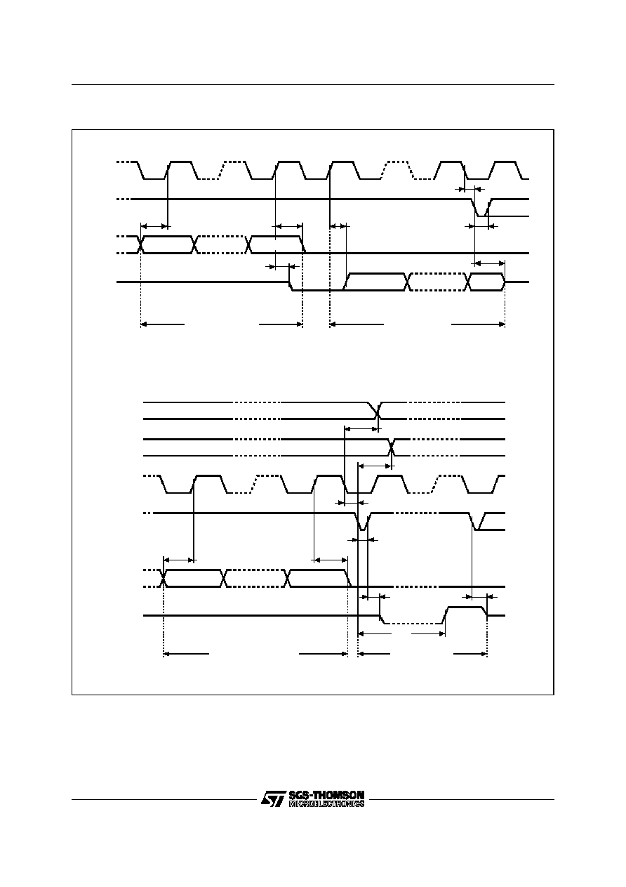
Figure 5. Synchronous Timing, Read or Write
AI00820C
C
D
Q
ADDRESS INPUT
Hi-Z
tDVCH
tCLSL
A0
S
DATA OUTPUT
tCHQV
tCHDX
tCHQL
An
tSLSH
tSLQZ
Q15/Q7
Q0
PRE
W
C
S
D
Hi-Z
tW
tDVCH
AI00888B
Q
tCLPRX
tSLWX
tCLSL
tCHDX
tSLSH
tSLQZ
BUSY
tSHQV
READY
WRITE CYCLE
ADDRESS/DATA INPUT
An
A0/D0
5/16
ST93CS46, ST93CS47