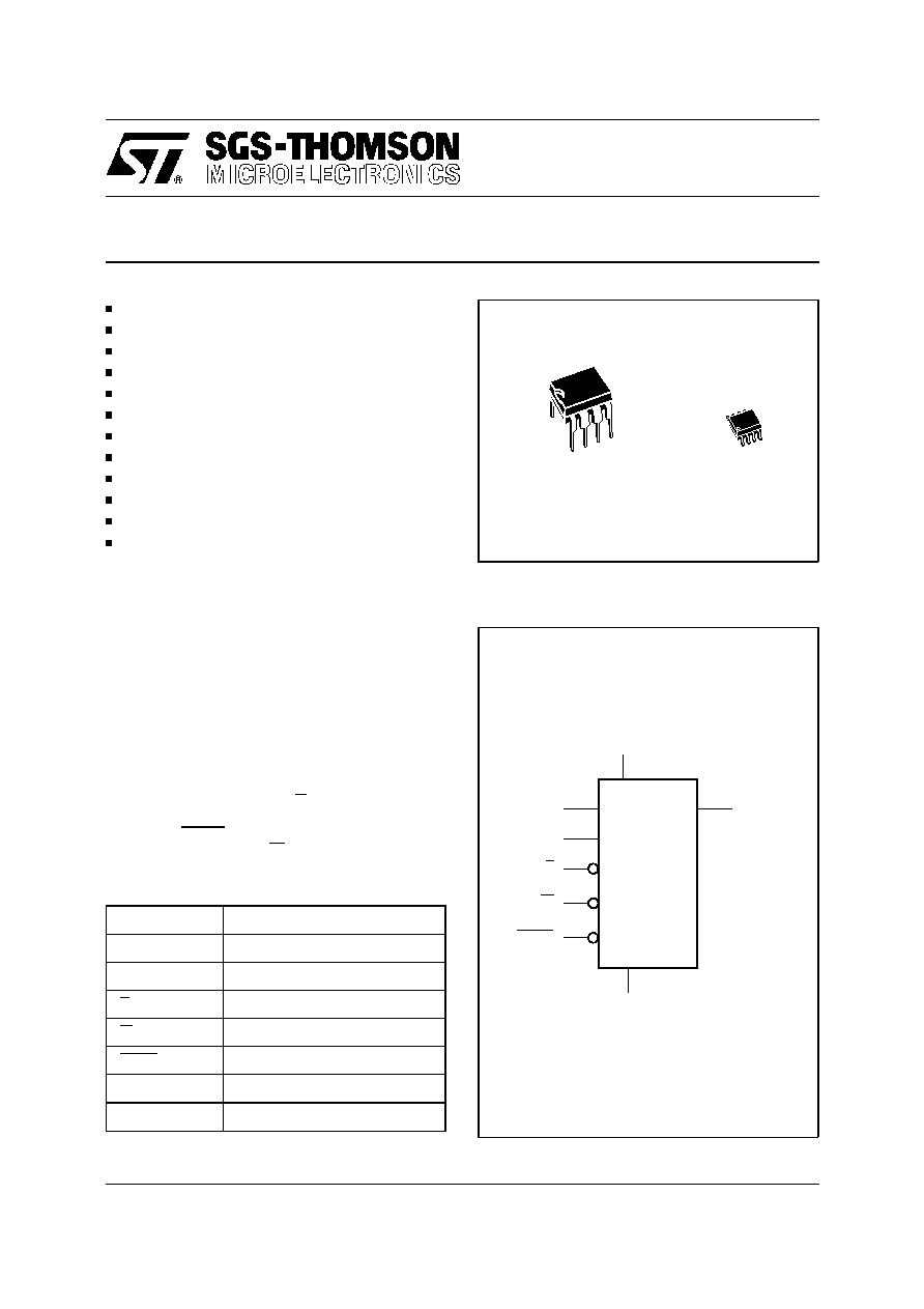
AI01063B
S
VCC
ST95P04
HOLD
VSS
W
Q
C
D
Figure 1. Logic Diagram
ST95P04
SERIAL ACCESS SPI BUS 4K (512 x 8) EEPROM
NOT FOR NEW DESIGN
1 MILLION ERASE/WRITE CYCLES
40 YEARS DATA RETENTION
SINGLE 3V to 5.5V SUPPLY VOLTAGE
SPI BUS COMPATIBLE SERIAL INTERFACE
1 MHz CLOCK RATE MAX
BLOCK WRITE PROTECTION
STATUS REGISTER
16 BYTE PAGE MODE
WRITE PROTECT
SELF-TIMED PROGRAMMING CYCLE
E.S.D.PROTECTION GREATER than 4000V
The ST95P04 will be replaced shortly by the
updated version ST95040
DESCRIPTION
The ST95P04 is a 4K bit Electrically Erasable
Programmable Memory (EEPROM) fabricated with
SGS-THOMSON's High Endurance Single Polysili-
con CMOS technology. The 4K bit memory is or-
ganised as 32 pages of 16 bytes. The memory is
accessed by a simple SPI bus compatible serial
interface. The bus signals are a serial clock input
(C), a serial data input (D) and a serial data output
(Q). The device connected to the bus is selected
when the chip select input (S) goes low. Commu-
nications with the chip can be interrupted with a
hold input (HOLD). The write operation is disabled
by a write protect input (W).
C
Serial Clock
D
Serial Data Input
Q
Serial Data Output
S
Chip Select
W
Write Protect
HOLD
Hold
V
CC
Supply Voltage
V
SS
Ground
Table 1. Signal Names
8
1
SO8 (M)
8
1
PSDIP8 (B)
0.25mm Frame
June 1996
1/16
Symbol
Parameter
Value
Unit
T
A
Ambient Operating Temperature
≠40 to 85
∞
C
T
STG
Storage Temperature
≠65 to 150
∞
C
T
LEAD
Lead Temperature, Soldering
(SO8 package)
(PSDIP8 package)
40 sec
10 sec
215
260
∞
C
V
O
Output Voltage
≠0.3 to V
CC
+0.6
V
V
I
Input Voltage
≠0.3 to 6.5
V
V
CC
Supply Voltage
≠0.3 to 6.5
V
V
ESD
Electrostatic Discharge Voltage (Human Body model)
(2)
4000
V
Electrostatic Discharge Voltage (Machine model)
(3)
500
V
Notes: 1. Except for the rating "Operating Temperature Range", stresses above those listed in the Table "Absolute Maximum Ratings"
may cause permanent damage to the device. These are stress ratings only and operation of the device at these or any other
conditions above those indicated in the Operating sections of this specification is not implied. Exposure to Absolute Maximum
Rating conditions for extended periods may affect device reliability. Refer also to the SGS-THOMSON SURE Program and
other relevant quality documents.
2. MIL-STD-883C, 3015.7 (100pF, 1500
)
3. EIAJ IC-121 (Condition C) (200pF, 0
)
Table 2. Absolute Maximum Ratings
(1)
SIGNALS DESCRIPTION
Serial Output (Q). The output pin is used to trans-
fer data serially out of the ST95P04. Data is shifted
out on the falling edge of the serial clock.
Serial Input (D). The input pin is used to transfer
data serially into the device. It receives instructions,
addresses, and data to be written. Input is latched
on the rising edge of the serial clock.
Serial Clock (C). The serial clock provides the
timing of the serial interface. Instructions, ad-
dresses, or data present at the input pin are latched
on the rising edge of the clock input, while data on
the Q pin changes after the falling edge of the clock
input.
Chip Select (S). This input is used to select the
ST95P04. The chip is selected by a high to low
transition on the S pin when C is at '0' state. At any
time, the chip is deselected by a low to high transi-
tion on the S pin when C is at '0' state. As soon as
the chip is deselected, the Q pin is at high imped-
ance state. This pin allows multiple ST95P04 to
share the same SPI bus. After power up, the chip
is at the deselect state. Transitions of S are ignored
when C is at '1' state.
D
VSS
C
HOLD
Q
S
VCC
W
AI01064B
ST95P04
1
2
3
4
8
7
6
5
Figure 2A. DIP Pin Connections
1
AI01065C
2
3
4
8
7
6
5
D
VSS
C
HOLD
Q
S
VCC
W
ST95P04
Figure 2B. SO Pin Connections
2/16
ST95P04
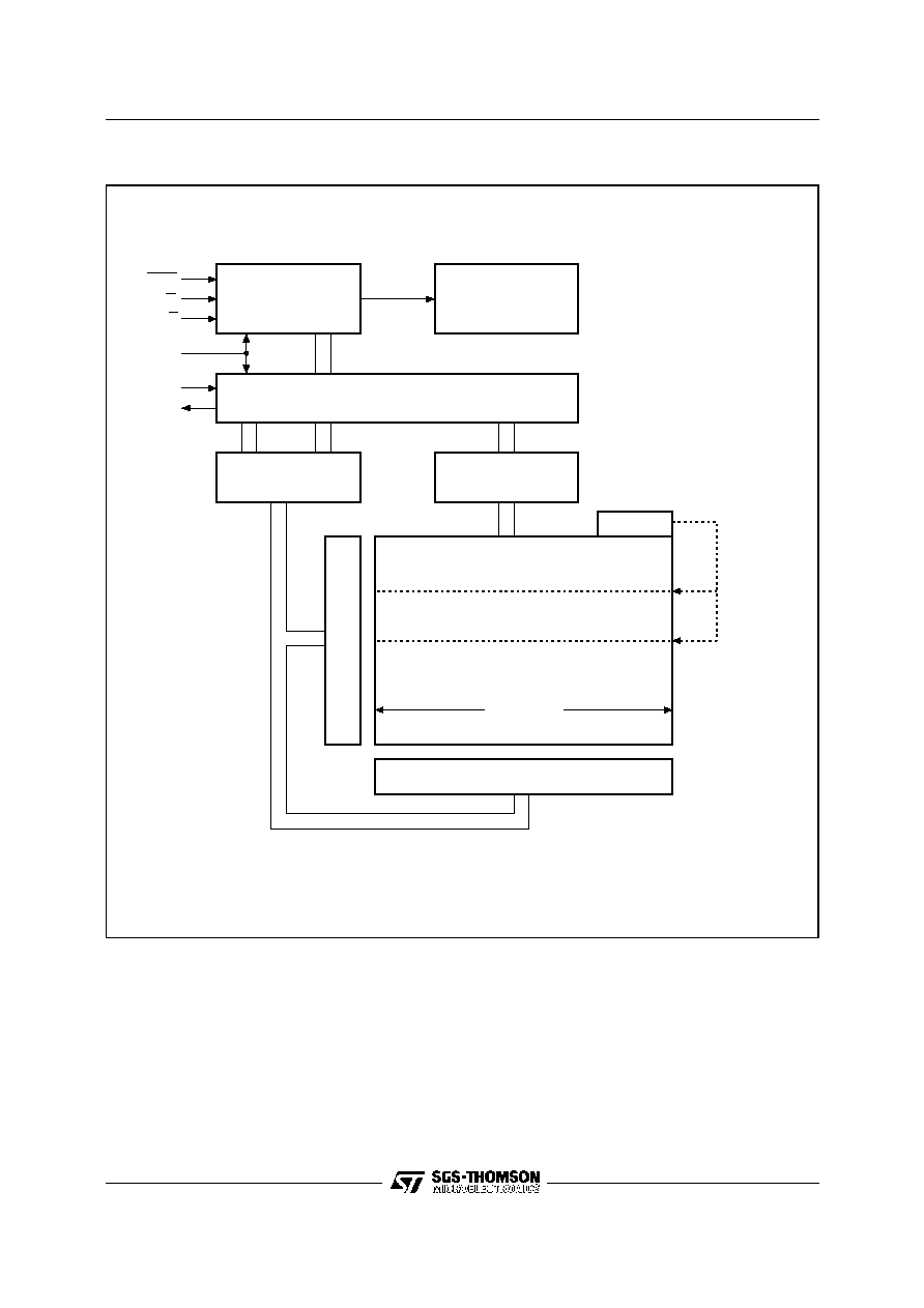
AI01272
HOLD
S
W
Control Logic
High Voltage
Generator
I/O Shift Register
Address Register
and Counter
Data
Register
16 Bytes
X Decoder
Y Decoder
Block
Protect
C
D
Q
Status
Figure 3. Block Diagram
3/16
ST95P04

AI00825
0.8VCC
0.2VCC
0.7VCC
0.3VCC
Figure 4. AC Testing Input Output Waveforms
Input Rise and Fall Times
50ns
Input Pulse Voltages
0.2V
CC
to 0.8V
CC
Input and Output Timing
Reference Voltages
0.3V
CC
to 0.7V
CC
AC MEASUREMENT CONDITIONS
Note that Output Hi-Z is defined as the point where data
is no longer driven.
Symbol
Parameter
Min
Max
Unit
C
IN
Input Capacitance (D)
8
pF
C
IN
Input Capacitance (other pins)
6
pF
t
LPF
Input Signal Pulse Width
10
ns
Note: 1. Sampled only, not 100% tested.
Table 3. Input Parameters
(1)
(T
A
= 25
∞
C, f = 1 MHz )
Symbol
Parameter
Test Condition
Min
Max
Unit
I
LI
Input Leakage Current
2
µ
A
I
LO
Output Leakage Current
±
2
µ
A
I
CC
V
CC
Supply Current (Active)
C = 0.1 V
CC
/0.9 V
CC
,
@ 1 MHz, Q = Open
2
mA
I
CC1
V
CC
Supply Current (Standby)
S = V
CC
, V
IN
= V
SS
or V
CC
,
V
CC
= 5.5V
50
µ
A
S = V
CC
, V
IN
= V
SS
or V
CC
,
V
CC
= 3V
10
µ
A
V
IL
Input Low Voltage
≠ 0.3
0.3 V
CC
V
V
IH
Input High Voltage
0.7 V
CC
V
CC
+ 1
V
V
OL
Output Low Voltage
I
OL
= 2mA
0.2 V
CC
V
V
OH
Output High Voltage
I
OH
= ≠2mA
0.8 V
CC
V
Table 4. DC Characteristics
(T
A
= 0 to 70
∞
C or ≠40 to 85
∞
C; V
CC
= 3V to 5.5V)
4/16
ST95P04
Symbol
Alt
Parameter
Test Condition
Min
Max
Unit
f
C
f
C
Clock Frequency
D.C.
1
MHz
t
SLCH
t
SU
S Setup Time
100
ns
t
CLSH
t
SH
S Hold Time
100
ns
t
CH
t
WH
Clock High Time
400
ns
t
CL
t
WL
Clock Low Time
400
ns
t
CLCH
t
RC
Clock Rise Time
1
µ
s
t
CHCL
t
FC
Clock Fall Time
1
µ
s
t
DVCH
t
DSU
Data In Setup Time
100
ns
t
CHDX
t
DH
Data In Hold Time
100
ns
t
DLDH
t
RI
Data In Rise Time
1
µ
s
t
DHDL
t
FI
Data In Fall Time
1
µ
s
t
HXCH
t
HSU
HOLD Setup Time
100
ns
t
CLHX
t
HH
HOLD Hold Time
100
ns
t
SHSL
t
CS
S Deselect Time
400
ns
t
SHQZ
t
DIS
Output Disable Time
300
ns
t
QVCL
t
V
Clock Low to Output Valid
400
ns
t
CLQX
t
HO
Output Hold Time
0
ns
t
QLQH
t
RO
Output Rise Time
150
ns
t
QHQL
t
FO
Output Fall Time
150
ns
t
HHQX
t
LZ
HOLD High to Output Low-Z
300
ns
t
HLQZ
t
HZ
HOLD Low to Output High-Z
300
ns
t
W
(1)
t
W
Write Cycle Time
10
ms
Note: 1. Not enough characterisation data were available on this parameter at the time of issue this Data Sheet. The typical value is well
below 5ms, the maximum value will be reviewed and lowered when sufficient data is available.
Table 5. AC Characteristics
(T
A
= 0 to 70
∞
C or ≠40 to 85
∞
C; V
CC
= 3V to 5.5V)
5/16
ST95P04
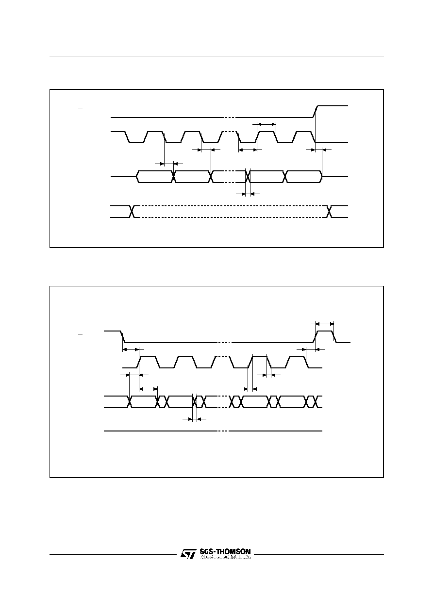
C
Q
AI01070B
S
MSB OUT
MSB-1 OUT
LSB OUT
D
ADDR.LSB IN
tSHQZ
tCH
tCL
tQLQH
tQHQL
tCLQX
tQVCL
Figure 5. Output Timing
C
D
AI01071
S
MSB IN
Q
tDVCH
HIGH IMPEDANCE
LSB IN
tSLCH
tCHDX
tDLDH
tDHDL
tCHCL
tCLCH
tCLSH
tSHSL
Figure 6. Serial Input Timing
6/16
ST95P04
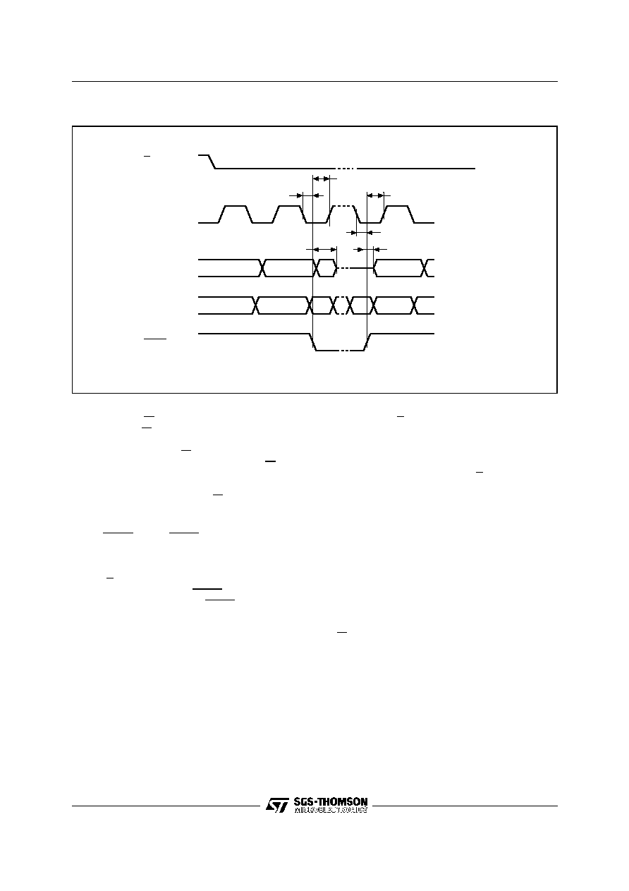
C
Q
AI01072B
S
D
HOLD
tCLHX
tHXCH
tHXCH
tCLHX
tHHQX
tHLQZ
Figure 7. Hold Timing
Write Protect (W). This pin is for hardware write
protect. When W is low, non-volatile writes to the
ST95P04 are disabled but any other operation
stays enabled. When W is high, all operations
including non-volatile writes are available. W going
low at any time before the last bit D0 of the data
stream will reset the write enable latch and prevent
programming. No action on W or on the write
enable latch can interrupt a write cycle which has
commenced.
Hold (HOLD). The HOLD pin is used to pause
serial communications with a ST95P04 without
resetting the serial sequence. To take the Hold
condition into account, the product must be se-
lected (S = 0). Then the Hold state is validated by
a high to low transition on HOLD when C is low. To
resume the communications, HOLD is brought high
when C is low. During Hold condition D, Q, and C
are at a high impedance state.
When the ST95P04 is under Hold condition, it is
possible to deselect it. However, the serial commu-
nications will remain paused after a reselect, and
the chip will be reset.
OPERATIONS
All instructions, addresses and data are shifted in
and out of the chip MSB first. Data input (D) is
sampled on the first rising edge of clock (C) after
the chip select (S) goes low. Prior to any operation,
a one-byte instruction code must be entered in the
chip. This code is entered via the data input (D),
and latched on the rising edge of the clock input
(C). To enter an instruction code, the product must
have been previously selected (S = low). Table 7
shows the instruction set and format for device
operation. When an invalid instruction is sent (one
not contained in Table 7), the chip is automatically
deselected. For operations that read or write data
in the memory array, bit 3 of the instruction is the
MSB of the address, otherwise, it is a don't care.
Write Enable (WREN) and Write Disable (WRDI)
The ST95P04 contains a write enable latch. This
latch must be set prior to every WRITE or WRSR
operation. The WREN instruction will set the latch
and the WRDI instruction will reset the latch. The
latch is reset under all the following conditions:
≠ W pin is low
≠ Power on
≠ WRDI instruction executed
≠ WRSR instruction executed
≠ WRITE instruction executed
As soon as the WREN or WRDI instruction is
received by the ST95P04, the circuit executes the
instruction and enters a wait mode until it is dese-
lected.
7/16
ST95P04
Read Status Register (RDSR)
The RDSR instruction provides access to the status
register. The status register may be read at any
time, even during a non-volatile write. As soon as
the 8th bit of the status register is read out, the
ST95P04 enters a wait mode (data on D are not
decoded, Q is in Hi-Z) until it is deselected.
The status register format is as follows:
b7
b0
1
1
1
1
BP1
BP0
WEL
WIP
BP1, BP0: Read and Write bits
WEL, WIP: Read only bits.
During a non-volatile write to the memory array, all
bits BP1, BP0, WEL, WIP are valid and can be read.
During a non volatile write to the status register, the
only bits WEL and WIP are valid and can be read.
The values of BP1 and BP0 read at that time
correspond to the previous contents of the status
register.
The Write-In-Process (WIP) read only bit indicates
whether the ST95P04 is busy with a write opera-
tion. When set to a '1' a write is in progress, when
set to a '0' no write is in progress.
The Write Enable Latch (WEL) read only bit indi-
cates the status of the write enable latch. When set
to a '1' the latch is set, when set to a '0' the latch is
reset.
The Block Protect (BP0 and BP1) bits indicate the
extent of the protection employed. These bits are
set by the user issuing the WRSR instruction.
These bits are non-volatile.
Write Status Register (WRSR)
The WRSR instruction allows the user to select the
size of protected memory. The ST95P04 is divided
into four 1024 bit blocks. The user may read the
blocks but will be unable to write within the selected
blocks.
The blocks and respective WRSR control bits are
shown in Table 6.
When the WRSR instruction and the 8 bits of the
Status Register are latched-in, the internal write
cycle is then triggered by the rising edge of S. This
rising edge of S must appear after the 8th bit of the
Status Register content (it must not appear a 17th
clock pulse before the rising edge of S), otherwise
the internal write sequence is not performed.
Read Operation
The chip is first selected by putting S low. The serial
one byte read instruction is followed by a one byte
address (A7-A0), each bit being latched-in during
the rising edge of the clock (C). Bit 3 of the read
instruction contains address A8 (most significant
address bit). This bit is used to select the first or
second page of the device. Then, the data stored
in the memory at the selected address is shifted out
on the Q output pin; each bit being shifted out
during the falling edge of the clock (C). The data
stored in the memory at the next address can be
read in sequence by continuing to provide clock
Status Register Bits
Array Addresses
Protected
BP1
BP0
0
0
none
0
1
180h - 1FFh
1
0
100h - 1FFh
1
1
000h - 1FFh
Table 6. Array Addresses Protect
Instruction
Description
Instruction Format
WREN
Set Write Enable Latch
0000 X110
WRDI
Reset Write Enable Latch
0000 X100
RDSR
Read Status Register
0000 X101
WRSR
Write Status Register
0000 X001
READ
Read Data from Memory Array
0000 A011
WRITE
Write Data to Memory Array
0000 A010
Table 7. Instruction Set
Notes: A = 1, Upper page selected
A = 0, Lower page selected
X = Don't care
8/16
ST95P04
pulses. The byte address is automatically incre-
mented to the next higher address after each byte
of data is shifted out. When the highest address is
reached (1FFh), the address counter rolls over to
0h allowing the read cycle to be continued indefi-
nitely. The read operation is terminated by dese-
lecting the chip. The chip can be deselected at any
time during data output. Any read attempt during a
non-volatile write cycle will be rejected and will
deselect the chip.
Byte Write Operation
Prior to any write attempt, the write enable latch
must have been set by issuing the WREN instruc-
tion. First, the device is selected (S = low) and a
serial WREN instruction byte is issued. Then, the
product is deselected by taking S high. After the
WREN instruction byte is sent, the ST95P04 will
set the write enable latch and then remain in
standby until it is deselected. Then, the write state
is entered by selecting the chip, issuing a one byte
address (A7-A0), and one byte of data. Bit 3 of the
write instruction contains address A8 (most signifi-
cant address bit). S must remain low for the entire
duration of the operation. The product must be
deselected just after the eigth bit of data has been
latched in. If not, the write process is cancelled. As
soon as the product is deselected, the self-timed
write cycle is initiated. While the write is in progress,
the status register may be read to check BP1, BP0,
WEL and WIP. WIP is high during the self-timed
write cycle. When the cycle is close to completion,
the write enable latch is reset.
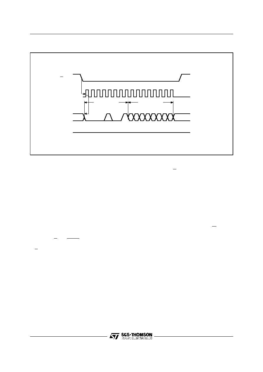
Page Write Operation
A maximum of 16 bytes of data may be written
during one non-volatile write cycle. All 16 bytes
must reside on the same page. The page write
mode is the same as the byte write mode except
that instead of deselecting after the first byte of
data, up to 15 additional bytes can be shifted in
prior to deselecting the chip. A page address begins
with address xxxx 0000 and ends with xxxx 1111.
If the address counter reaches xxxx 1111 and the
clock continues, the counter will roll over to the first
address of the page (xxxx 0000) and overwrite any
previous written data. The programming cycle will
only start if the S transition does occur at the clock
low pulse just after the eigth bit of data of a word is
received.
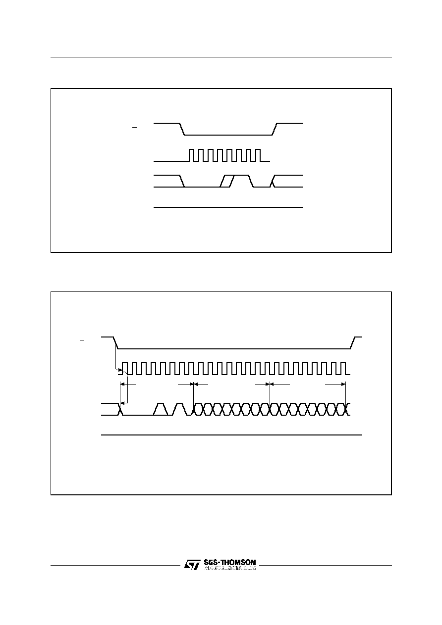
C
D
AI01066
S
Q
2
1
3
4
5
6
7
8
9 10 11 12 13 14 15 16 17 18 19
A
20 21 22 23
7
6
5
4
3
2
0
1
HIGH IMPEDANCE
DATA OUT
INSTRUCTION
BYTE ADDRESS
0
MSB
Figure 8. Read Operation Sequence
9/16
ST95P04
C
D
AI01068
S
Q
2
1
3
4
5
6
7
8
9 10 11 12 13 14 15 16 17 18 19 20 21 22 23
HIGH IMPEDANCE
INSTRUCTION
BYTE ADDRESS
0
7
6
5
4
3
2
0
1
DATA BYTE
A
Figure 10. Write Operation Sequence
C
D
AI01067
S
Q
2
1
3
4
5
6
7
HIGH IMPEDANCE
0
Figure 9. Write Enable Latch Sequence
10/16
ST95P04
C
D
S
2
1
3
4
5
6
7
8
9 10 11 12 13 14 15 16 17 18 19 20 21 22 23
INSTRUCTION
BYTE ADDRESS
0
7
6
5
4
3
2
0
1
DATA BYTE 1
C
D
AI01069
S
7
26
25
27 28 29 30 31
8+8N
6
3
2
1
0
24
7
6
5
4
3
2
1
DATA BYTE 16
9+8N
10+8N
11+8N
12+8N
13+8N
14+8N
15+8N
136
137
138
139
140
141
142
143
5
4
0
DATA BYTE N
7
6
3
2
1
0
5
4
DATA BYTE 2
7
A
Figure 11. Page Write Operation Sequence
C
D
S
2
1
3
4
5
6
7
8
9 10 11 12 13 14 15
INSTRUCTION
0
AI01433
Q
7
6
5
4
3
2
1
0
STATUS REG. OUT
HIGH IMPEDANCE
MSB
Figure 12. RDSR: Read Status Register Sequence
11/16
ST95P04
POWER ON STATE
After a Power up the ST95P04 is in the following
state:
≠ The device is in the low power standby state.
≠ The chip is deselected.
≠ The chip is not in hold condition.
≠ The write enable latch is reset.
≠ BP1 and BP0 are unchanged (non-volatile
bits).
DATA PROTECTION AND PROTOCOL SAFETY
≠ All inputs are protected against noise, see Ta-
ble 3.
≠ Non valid S and HOLD transitions are not
taken into account.
≠ S must come high at the proper clock count in
order to start a non-volatile write cycle (in the
memory array or in the cycle status register).
The Chip Select S must rise during the clock
pulse following the introduction of a multiple of
8 bits.
≠ Access to the memory array during non-vola-
tile programming cycle is cancelled and the
chip is automatically deselected; however, the
programming cycle continues.
≠ After either of the following operations
(WREN, WRDI, RDSR) is completed, the chip
enters a wait state and waits for a deselect.
≠ The write enable latch is reset upon power-up.
≠ The write enable latch is reset when W is
brought low.
INITIAL DELIVERY STATE
The device is delivered with the memory array in a
fully erased state (all data set at all "1's" or FFh).
The block protect bits are initialized to 00.
C
D
AI01434
S
Q
2
1
3
4
5
6
7
8
9 10 11 12 13 14 15
HIGH IMPEDANCE
INSTRUCTION
STATUS REG.
0
Figure 13. WRSR: Write Status Register Sequence
12/16
ST95P04
ORDERING INFORMATION SCHEME
For a list of available options (Package, Temperature Range, etc...) refer to the current Memory Shortform
catalogue.
For further information on any aspect of this device, please contact the SGS-THOMSON Sales Office
nearest to you.
Notes: P * Data In strobed on rising edge of the clock (C) and Data Out synchronized from the falling edge of the clock.
3 * Temperature range on special request only.
Data Strobe
P *
D Q
Package
B
PSDIP8
0.25 mm Frame
M
SO8
1501mil Width
Temperature Range
1
0 to 70
∞
C
6
≠40 to 85
∞
C
3 *
≠40 to 125
∞
C
Option
TR
Tape & Reel
Packing
Example: ST95P04 M 6 TR
13/16
ST95P04
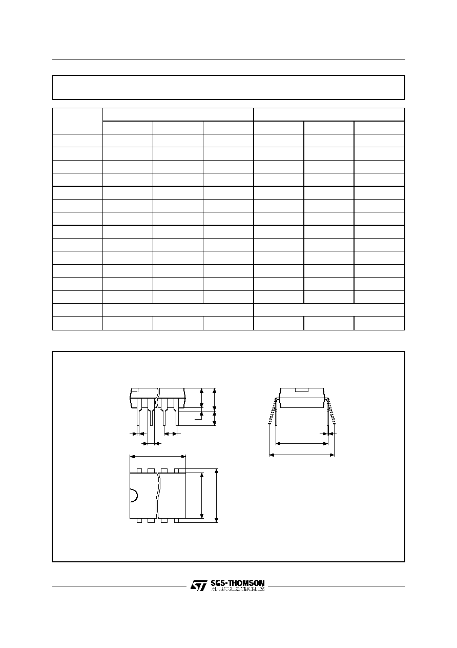
PSDIP-a
A2
A1
A
L
e1
D
E1
E
N
1
C
eA
eB
B1
B
Symb
mm
inches
Typ
Min
Max
Typ
Min
Max
A
3.90
5.90
0.154
0.232
A1
0.49
≠
0.019
≠
A2
3.30
5.30
0.130
0.209
B
0.36
0.56
0.014
0.022
B1
1.15
1.65
0.045
0.065
C
0.20
0.36
0.008
0.014
D
9.20
9.90
0.362
0.390
E
7.62
≠
≠
0.300
≠
≠
E1
6.00
6.70
0.236
0.264
e1
2.54
≠
≠
0.100
≠
≠
eA
7.80
≠
0.307
≠
eB
10.00
0.394
L
3.00
3.80
0.118
0.150
N
8
8
CP
0.10
0.004
PSDIP8
Drawing is not to scale
PSDIP8 - 8 pin Plastic Skinny DIP, 0.25mm lead frame
14/16
ST95P04
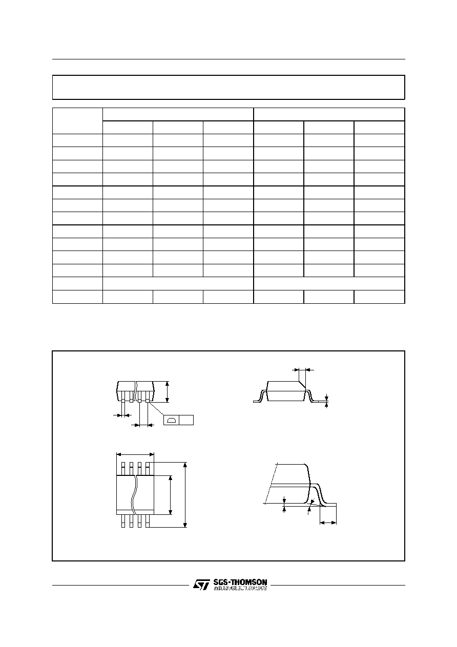
SO-a
E
N
CP
B
e
A
D
C
L
A1
1
H
h x 45∞
Symb
mm
inches
Typ
Min
Max
Typ
Min
Max
A
1.35
1.75
0.053
0.069
A1
0.10
0.25
0.004
0.010
B
0.33
0.51
0.013
0.020
C
0.19
0.25
0.007
0.010
D
4.80
5.00
0.189
0.197
E
3.80
4.00
0.150
0.157
e
1.27
≠
≠
0.050
≠
≠
H
5.80
6.20
0.228
0.244
h
0.25
0.50
0.010
0.020
L
0.40
0.90
0.016
0.035
0
∞
8
∞
0
∞
8
∞
N
8
8
CP
0.10
0.004
SO8
Drawing is not to scale
SO8 - 8 lead Plastic Small Outline, 150 mils body width
15/16
ST95P04

Information furnished is believed to be accurate and reliable. However, SGS-THOMSON Microelectronics assumes no responsibility for the
consequences of use of such information nor for any infringement of patents or other rights of third parties which may result from its use. No
license is granted by implication or otherwise under any patent or patent rights of SGS-THOMSON Microelectronics. Specifications mentioned
in this publication are subject to change without notice. This publication supersedes and replaces all information previously supplied.
SGS-THOMSON Microelectronics products are not authorized for use as critical components in life support devices or systems without express
written approval of SGS-THOMSON Microelectronics.
© 1996 SGS-THOMSON Microelectronics - All Rights Reserved
SGS-THOMSON Microelectronics GROUP OF COMPANIES
Australia - Brazil - China - France - Germany - Hong Kong - Italy - Japan - Korea - Malaysia - Malta - Morocco - The Netherlands -
Singapore - Spain - Sweden - Switzerland - Taiwan - Thailand - United Kingdom - U.S.A.
16/16
ST95P04