AI01256
S
VCC
ST95P02
HOLD
VSS
W
Q
C
D
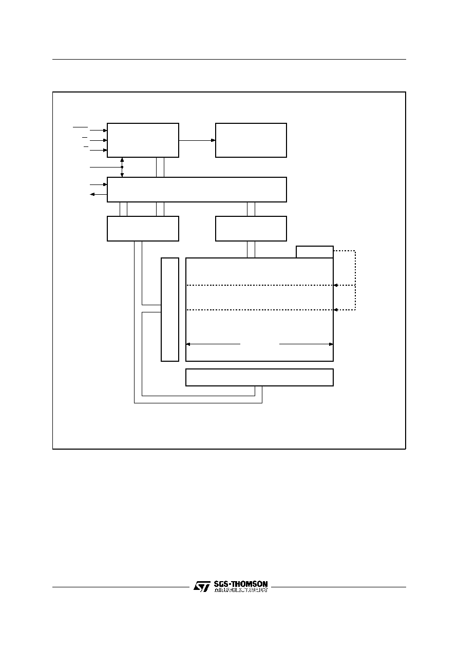
Figure 1. Logic Diagram
ST95P02
SERIAL ACCESS SPI BUS 2K (256 x 8) EEPROM
NOT FOR NEW DESIGN
1 MILLION ERASE/WRITE CYCLES
40 YEARS DATA RETENTION
SINGLE 3V to 5.5V SUPPLY VOLTAGE
SPI BUS COMPATIBLE SERIAL INTERFACE
2 MHz CLOCK RATE MAX
BLOCK WRITE PROTECTION
STATUS REGISTER
16 BYTE PAGE MODE
WRITE PROTECT
SELF-TIMED PROGRAMMING CYCLE
E.S.D.PROTECTION GREATER than 4000V
The ST95P02 will be replaced shortly by the
updated version ST95020
DESCRIPTION
The ST95P02 is a 2K bit Electrically Erasable
Programmable Memory (EEPROM) fabricated with
SGS-THOMSON's High Endurance Single Polysili-
con CMOS technology. The 2K bit memory is or-
ganised as 16 pages of 16 bytes. The memory is
accessed by a simple SPI bus compatible serial
interface. The bus signals are a serial clock input
(C), a serial data input (D) and a serial data output
(Q). The device connected to the bus is selected
when the chip select input (S) goes low. Commu-
nications with the chip can be interrupted with a
hold input (HOLD). The write operation is disabled
by a write protect input (W).
C
Serial Clock
D
Serial Data Input
Q
Serial Data Output
S
Chip Select
W
Write Protect
HOLD
Hold
V
CC
Supply Voltage
V
SS
Ground
Table 1. Signal Names
8
1
SO8 (M)
8
1
PSDIP8 (B)
0.25mm Frame
June 1996
1/16
Symbol
Parameter
Value
Unit
T
A
Ambient Operating Temperature
≠40 to 85
∞
C
T
STG
Storage Temperature
≠65 to 150
∞
C
T
LEAD
Lead Temperature, Soldering
(SO8 package)
(PSDIP8 package)
40 sec
10 sec
215
260
∞
C
V
O
Output Voltage
≠0.3 to V
CC
+0.6
V
V
I
Input Voltage
≠0.3 to 6.5
V
V
CC
Supply Voltage
≠0.3 to 6.5
V
V
ESD
Electrostatic Discharge Voltage (Human Body model)
(2)
4000
V
Electrostatic Discharge Voltage (Machine model)
(3)
500
V
Notes: 1. Except for the rating "Operating Temperature Range", stresses above those listed in the Table "Absolute Maximum Ratings"
may cause permanent damage to the device. These are stress ratings only and operation of the device at these or any other
conditions above those indicated in the Operating sections of this specification is not implied. Exposure to Absolute Maximum
Rating conditions for extended periods may affect device reliability. Refer also to the SGS-THOMSON SURE Program and
other relevant quality documents.
2. MIL-STD-883C, 3015.7 (100pF, 1500
)
3. EIAJ IC-121 (Condition C) (200pF, 0
)
Table 2. Absolute Maximum Ratings
(1)
SIGNALS DESCRIPTION
Serial Output (Q). The output pin is used to trans-
fer data serially out of the ST95P02. Data is shifted
out on the falling edge of the serial clock.
Serial Input (D). The input pin is used to transfer
data serially into the device. It receives instructions,
addresses, and data to be written. Input is latched
on the rising edge of the serial clock.
Serial Clock (C). The serial clock provides the
timing of the serial interface. Instructions, ad-
dresses, or data present at the input pin are latched
on the rising edge of the clock input, while data on
the Q pin changes after the falling edge of the clock
input.
Chip Select (S). This input is used to select the
ST95P02. The chip is selected by a high to low
transition on the S pin when C is at '0' state. At any
time, the chip is deselected by a low to high transi-
tion on the S pin when C is at '0' state. As soon as
the chip is deselected, the Q pin is at high imped-
ance state. This pin allows multiple ST95P02 to
share the same SPI bus. After power up, the chip
is at the deselect state. Transitions of S are ignored
when C is at '1' state.
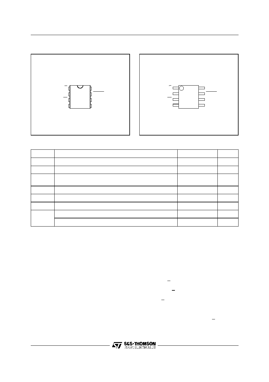
D
VSS
C
HOLD
Q
S
VCC
W
AI01257
ST95P02
1
2
3
4
8
7
6
5
Figure 2A. DIP Pin Connections
1
AI01258B
2
3
4
8
7
6
5
D
VSS
C
HOLD
Q
S
VCC
W
ST95P02
Figure 2B. SO Pin Connections
2/16
ST95P02
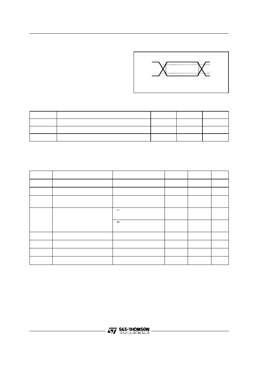
AI00825
0.8VCC
0.2VCC
0.7VCC
0.3VCC
Figure 4. AC Testing Input Output Waveforms
Input Rise and Fall Times
50ns
Input Pulse Voltages
0.2V
CC
to 0.8V
CC
Input and Output Timing
Reference Voltages
0.3V
CC
to 0.7V
CC
AC MEASUREMENT CONDITIONS
Note that Output Hi-Z is defined as the point where data
is no longer driven.
Symbol
Parameter
Min
Max
Unit
C
IN
Input Capacitance (D)
8
pF
C
IN
Input Capacitance (other pins)
6
pF
t
LPF
Input Signal Pulse Width
10
ns
Note: 1. Sampled only, not 100% tested.
Table 3. Input Parameters
(1)
(T
A
= 25
∞
C, f = 1 MHz )
Symbol
Parameter
Test Condition
Min
Max
Unit
I
LI
Input Leakage Current
2
µ
A
I
LO
Output Leakage Current
±
2
µ
A
I
CC
V
CC
Supply Current (Active)
C = 0.1 V
CC
/0.9 V
CC
,
@ 2 MHz, Q = Open
2
mA
I
CC1
V
CC
Supply Current (Standby)
S = V
CC
, V
IN
= V
SS
or V
CC
,
V
CC
= 5.5V
50
µ
A
S = V
CC
, V
IN
= V
SS
or V
CC
,
V
CC
= 3V
10
µ
A
V
IL
Input Low Voltage
≠ 0.3
0.3 V
CC
V
V
IH
Input High Voltage
0.7 V
CC
V
CC
+ 1
V
V
OL
Output Low Voltage
I
OL
= 2mA
0.2 V
CC
V
V
OH
Output High Voltage
I
OH
= ≠2mA
0.8 V
CC
V
Table 4. DC Characteristics
(T
A
= 0 to 70
∞
C or ≠40 to 85
∞
C; V
CC
= 3V to 5.5V)
4/16
ST95P02
Symbol
Alt
Parameter
Test Condition
Min
Max
Unit
f
C
f
C
Clock Frequency
D.C.
2
MHz
t
SLCH
t
SU
S Setup Time
50
ns
t
CLSH
t
SH
S Hold Time
50
ns
t
CH
t
WH
Clock High Time
200
ns
t
CL
t
WL
Clock Low Time
300
ns
t
CLCH
t
RC
Clock Rise Time
1
µ
s
t
CHCL
t
FC
Clock Fall Time
1
µ
s
t
DVCH
t
DSU
Data In Setup Time
50
ns
t
CHDX
t
DH
Data In Hold Time
50
ns
t
DLDH
t
RI
Data In Rise Time
1
µ
s
t
DHDL
t
FI
Data In Fall Time
1
µ
s
t
HXCH
t
HSU
HOLD Setup Time
50
ns
t
CLHX
t
HH
HOLD Hold Time
50
ns
t
SHSL
t
CS
S Deselect Time
4.5V < V
CC
< 5.5V
200
ns
3V < V
CC
< 4.5V
250
ns
t
SHQZ
t
DIS
Output Disable Time
150
ns
t
QVCL
t
V
Clock Low to Output Valid
300
ns
t
CLQX
t
HO
Output Hold Time
0
ns
t
QLQH
t
RO
Output Rise Time
100
ns
t
QHQL
t
FO
Output Fall Time
100
ns
t
HHQX
t
LZ
HOLD High to Output Low-Z
150
ns
t
HLQZ
t
HZ
HOLD Low to Output High-Z
150
ns
t
W
(1)
t
W
Write Cycle Time
10
ms
Note: 1. Not enough characterisation data were available on this parameter at the time of issue this Data Sheet. The typical value is well
below 5ms, the maximum value will be reviewed and lowered when sufficient data is available.
Table 5. AC Characteristics
(T
A
= 0 to 70
∞
C or ≠40 to 85
∞
C; V
CC
= 3V to 5.5V)
5/16
ST95P02