 | –≠–ª–µ–∫—Ç—Ä–æ–Ω–Ω—ã–π –∫–æ–º–ø–æ–Ω–µ–Ω—Ç: STA002 | –°–∫–∞—á–∞—Ç—å:  PDF PDF  ZIP ZIP |
FRONT_END INTERFACE:
IF input carrier frequency: f = 1.84 MHz
Single internal 6 bit A/D converter
QPSK demodulation
Input symbol frequency: Fs = 1.84 Msymbols/s
Digital Nyquist root filter:
- roll-off value of 0.4
Digital carrier loop:
- on-chip quadrature demodulator and tracking
loop
- lock detector
- C/N indicator
Digital timing recovery:
- internal timing error evaluation, filter and
correction
Digital AGC:
- internal signal power estimation and filter
- output control signal for AGC (1 bit PWM)
FORWARD ERROR CORRECTION:
Inner decoder:
- Viterbi soft decoder for convolutional codes,
constraint length M=7, Rate 1/2
Deinterleaver block
Outer decoder:
- Reed-Solomon decoder for 32 parity bytes;
correction of up to 16 byte errors
- Block lengths: 255
- Energy dispersal descrambler
BACK_END INTERFACE:
Broadcast Channel selection
Audio Service Component selection to MPEG
decoder
Service Component selection
CONTROL:
I
2
C serial Bus control interface
DECRYPTION:
WES scheme supported
DESCRIPTION
Designed for World Space satellites digital audio
receivers, the STA002 Digital Receiver Front-end
integrates all the blocks needed to demodulate
incoming digital satellite audio signals from the
tuner: analog to digital converter, QPSK demodu-
lator, signal power estimator, automatic gain con-
trol, Viterbi decoder, deinterleaver, Reed-Solo-
mon decoder and energy dispersal descrabler. Its
advanced error correction functions guarantees a
low error rate even with small low gain receiver
antennas.
Additional functions include the selection of
broadcast channel, service components and
audio components for source decoding:
- The MPEG Audio bitstream is provided at the
serial audio output port.
- The Broadcast Channel is provided to the serial
data output port.
- The Service Component is provided at the SC
output interface.
World Space encryption scheme is supported for
pay programs and paging.
January 2002
Æ
TQFP44
STA002
STARMAN
TM
CHANNEL DECODER
1/43
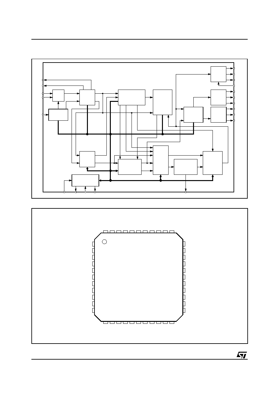
A/D
QPSK
LOCK
AGC
TDM FRAME
CONTROLLER
FRAME
SYNC.
TSCC
MANAGEMENT
PRC
MANAGEMENT
TDM_CLK
TDM
VITERBI
DE-INTERLEAVER
REED
SOLOMON
SOURCE
DECODER
INTERFACE
MICROPROCESSOR
INTERFACE
SCL
M_CLK
SCK
D96AU541C
RXI
RNXI
SDA
SC
MANGEMENT
BC_CLK
BC
SC
DATA
INTERFACE
SDO
SEN
SCEN
SCDO
SCCK
BC/TSCC
INTR
RESET
MINTR
BC
DATA
INTERFACE
BCCK
BCDO
BCSYNC
BCDIN
PLL/CLOCK
DISTRIBUTION
Fig. 1: Channel Decoder Block Diagram
D97AU671A
1
2
3
5
6
4
7
8
9
10
17
11
18
19
20
21
22
44
43
42
41
39
40
38
37
36
35
34
28
27
26
24
23
25
33
32
31
29
30
NRXI
RXI
A_VDD
AGC
TEST 1
VDD
12
13
14
15
16
A_GND
M_CLK
GND
CLK_TEST
TEST 2
TEST 3
LOCK
VDD
SDA
SCL
GND
TEST 4
VDD
GND
INTR
RESET
TEST 5
SCK
SEN
VDD
MINTR
TEST 6
TEST 7
BCDIN
BCSYNC
GND
SDO
SCEN
VDD
BCDO
BCCK
TEST 8
GND
VDD
SCCK
GND
TEST 9
SCDO
Fig. 2: Pin Connection
STA002
2/43
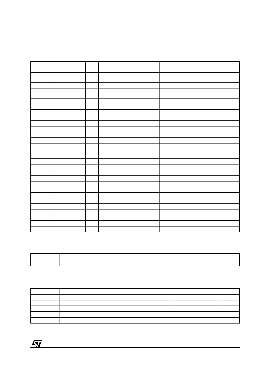
PIN DESCRIPTION
Type
Pin Name
Type
Function
PAD Description
1, 11, 12
TEST (1:3)
I
Test Pin
CMOS Input Pad Buffer with Pull-Down
22
23, 25, 33, 34, 44
TEST
(4:9)
I
Test Pin
2
AGC
O
AGC Output
CMOS 2mA Output Driver
3, 14, 21,
26, 38, 40
VDD
Positive Supply Voltage
4
A_VDD
Analog Positive Supply Voltage
5
RXI
I
IF Signal Input
Analog Pad Buffer
6
NRXI
I
IF Signal Input
Analog Pad Buffer
7
A_GND
Analog Ground
9
M_CLK
I
Master Clock
Analog Pad Buffer with Comparator
10
CLK_TEST
Not Connected
CMOS Input Pad Buffer
13
LOCK
O
Carrrier Lock Indicator
CMOS 2mA Output Driver
15
SDA
I/O
Data + ACK
CMOS Schmitt Trigger Bdir Pad Bufer
16
SCL
I
Serial Clock
CMOS Input Pad Schmitt Triggered
8, 17, 19,
30, 35, 42
GND
Negative Supply Voltage
18
INTR
O
Interrupt
CMOS 2mA Output Driver
20
RESET
I
Master Reset
CMOS Input Pad Buffer with Pull-Up
24
MINTR
O
MPEG Interrupt
CMOS 2mA Output Driver
27
SEN
O
MPEG Enable
CMOS 2mA Output Driver
28
SCK
O
MPEG Clock
CMOS 2mA Output Driver
29
SDO
O
MPEG Bit Output
CMOS 2mA Output Driver
31
BCSYNC
O
Broadcast Channel Sync
CMOS 2mA Output Driver
32
BCDIN
I
Broadcast Channel Data Input
CMOS Input Pad Buffer
36
BCCK
O
Broadcast Channel Clock
CMOS 2mA Output Driver
37
BCDO
O
Broadcast Channel Data Output
CMOS 2mA Output Driver
39
SCEN
O
Service Component Enable
CMOS 2mA Output Driver
41
SCCK
O
Service Component Clock
CMOS 2mA Output Driver
43
SCDO
O
Service Component Data Output
CMOS 2mA Output Driver
Note: pin 1, 11, 12 and 22 must be connected to ground in functional mode.
THERMAL DATA
Symbol
Parameter
Value
Unit
R
th j-amb
Thermal resistance Junction to Ambient
85
∞C/W
ABSOLUTE MAXIMUM RATINGS
Symbol
Parameter
Value
Unit
V
DD
Power Supply
-0.3 to 4
V
V
i
Voltage on Input pins
-0.3 to V
DD
+0.3
V
V
O
Voltage on output pins
-0.3 to V
DD
+0.3
V
T
stg
Storage Temperature
-40 to +150
∞C
T
oper
Operative ambient temp
-20 to +85
∞C
STA002
3/43
ELECTRICAL CHARACTERISTICS: V
DD
= 3.3V
±
0.3V; T
amb
= 0 to 70∞C; Rg = 50
unless otherwise
specified
DC OPERATING CONDITIONS
Symbol
Parameter
Value
V
DD
Power Supply Voltage
2.7 to 3.6V
T
j
Operating Junction Temperature
-20 to 125∞C
GENERAL INTERFACE ELECTRICAL CHARACTERISTICS
Symbol
Parameter
Test Condition
Min.
Typ.
Max.
Unit
Note
I
IL
Low Level Input Current
Without pull-up device
V
i
= 0V
-10
10
µ
A
1
I
IH
High Level Input Current
Without pull-up device
V
i
= V
DD
-10
10
µ
A
1
V
esd
Electrostatic Protection
Leakage < 1
µ
A
2000
V
2
Note 1: The leakage currents are generally very small, < 1nA. The value given here is a maximum that can occur after an electrostatic stress
on the pin.
Note 2: Human Body Model.
DC ELECTRICAL CHARACTERISTICS
Symbol
Parameter
Test Condition
Min.
Typ.
Max.
Unit
Note
V
IL
Low Level Input Voltage
0.2*V
DD
V
V
IH
High Level Input Voltage
0.8*V
DD
V
V
ol
Low Level Output Voltage
I
ol
= Xma
0.4V
V
1, 2
V
oh
High Level Output Voltage
0.85*V
DD
V
1, 2
Note 1: Takes into account 200mV voltage drop in both supply lines.
Note 2: X is the source/sink current under worst case conditions and is reflected in the name of the I/O cell according to the drive capability.
PULL_UP & PULL_DOWN CHARACTERISTICS
Symbol
Parameter
Test Condition
Min.
Typ.
Max.
Unit
Note
I
pu
Pull-up current
V
i
= 0V
-25
-66
-125
µ
A
1
I
pu
Pull-up current
V
i
= V
DD
25
66
125
µ
A
1
R
pu
Equivalent Pull-up
Resistance
V
i
= 0V
50
k
R
pu
Equivalent Pull-down
Resistance
V
i
= V
DD
50
k
Note 1: Min. condition: V
DD
= 2.7V, 125∞C Min process
Max. condition: V
DD
= 3.6V, -20∞C Max.
M_ CLK Electrical Characteristics (Pin number 9)
Symbol
Parameter
Min.
Typ.
Max.
Unit
V
il
Low Level Input Voltage
V
DD
-1.7
V
V
ih
High Level Input Voltage
V
DD
-0.9
V
V
ref
Input Reference Voltage
V
DD
-1.3
V
POWER DISSIPATION
Symbol
Parameter
Test Condition
Min.
Typ.
Max.
Unit
Note
PD
Power Dissipation
@ V
DD
= 3V
M_CLK = 39,0269MHz
80
mW
STA002
4/43

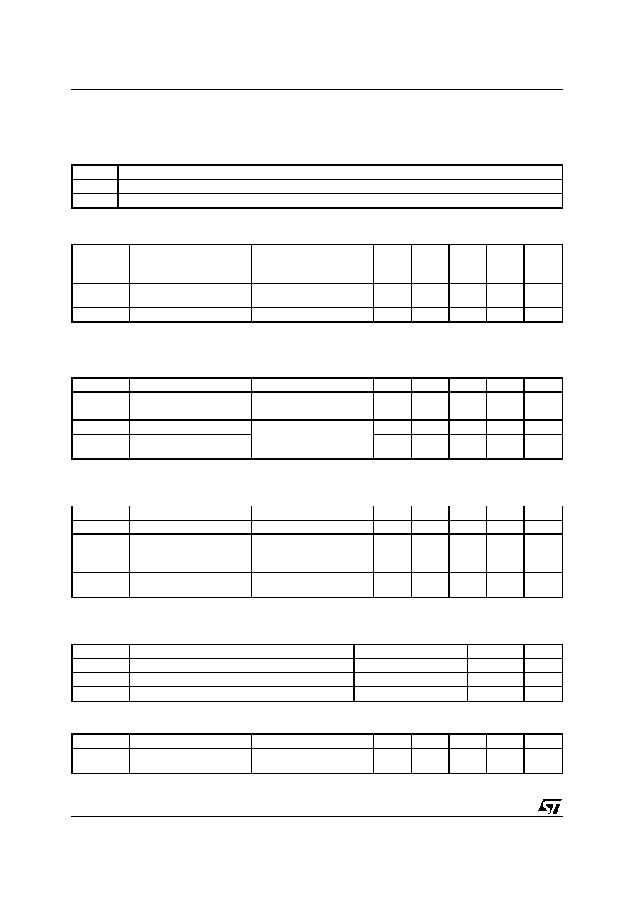
1
44
43
TEST9
SCDI
200
41
SCCK
200
200
39
SEN
200
37
BCDO
200
36
BCCK
BCSYNC
200
31
200
29
SDI
200
28
SCK
200
27
SEN
200
24
MINTR
200
18
INTR
AGC
200
13
200
2
3
8
5
6
9
10
11
34
TEST8
33
TEST7
32
BCDIN
25
TEST6
23
TEST5
22
TEST4
20
RESET
16
SCL
12
TEST3
15
SDA
100nF
4.7
µ
F
4.7
µ
F
100nF
100nF
100nF
100nF
100nF
14
17
100nF
21
19
100nF
26
30
100nF
38
35
100nF
40
42
4
7
100nF
VDD
V
SS
V
SS
V
SS
AV
SS
AV
SS
AV
SS
4.7
µ
F
4.7
µ
F
100nF
D99AU1011
100nF
100nF
100nF
100nF
AVDD
VDD
VDD
VDD
VDD
VDD
VDD
AVDD
RXI
NRXI
M_CLK
TEST_CLK
TEST2
TEST1
LOCK
Fig. 3: Test Circuit
I
OL
I
OH
C
L
V
REF
V
DD
OUTPUT
D98AU967
Figure 4. Test Load Circuit
Output
I
OL
I
OH
C
L
V
REF
SDA
5mA
100pF
3.6V
Other Outputs
100
µ
A
100
µ
A
100pF
1.5V
Test Load
STA002
5/43