 | –≠–ª–µ–∫—Ç—Ä–æ–Ω–Ω—ã–π –∫–æ–º–ø–æ–Ω–µ–Ω—Ç: STA003T | –°–∫–∞—á–∞—Ç—å:  PDF PDF  ZIP ZIP |
January 2002
SO28
SINGLE CHIP MPEG2 LAYER 3 DECODER
SUPPORTING:
- All features specified for Layer III in ISO/IEC
11172-3 (MPEG 1 Audio) except 44.1KHz
Audio
- All features specified for Layer III 2 channels
in ISO/IEC13818-3.2 (MPEG 2 Audio) except
22.05KHz Audio
- Lower sampling frequencies syntax extension,
(not specified by ISO) called MPEG 2.5
except 11.025KHz Audio
DECODES LAYER III STEREO CHANNELS,
DUAL CHANNEL, SINGLE CHANNEL
(MONO)
SUPPORTING THE MPEG 1 & 2 SAMPLING
FREQUENCIES AND THE EXTENSION TO
MPEG 2.5:
48, 32, 24, 16, 12, 8 KHz
ACCEPTS MPEG 2.5 LAYER III ELEMEN-
TARY COMPRESSED BITSTREAM WITH
DATA RATE FROM 8 Kbit/s UP TO 128 Kbit/s
DIGITAL VOLUME CONTROL
DIGITAL BASS & TREBLE CONTROL
SERIAL BITSTREAM INPUT INTERFACE
ANCILLARY DATA EXTRACTION VIA I2C IN-
TERFACE.
SERIAL PCM OUTPUT INTERFACE (I
2
S
AND OTHER FORMATS)
PLL FOR INTERNAL CLOCK AND FOR OUT-
PUT PCM CLOCK GENERATION
LOW POWER DATA ELABORATION FOR
POWER CONSUMPTION OPTIMISATION
CRC CHECK AND SYNCHRONISATION ER-
ROR DETECTION WITH SOFTWARE INDI-
CATORS
I
2
C CONTROL BUS
LOW POWER 3.3V CMOS TECHNOLOGY
14.72MHz EXTERNAL INPUT CLOCK OR
BUILT-IN XTAL OSCILLATOR
APPLICATIONS
STARMAN SATELLITE RADIO RECEIVER
DESCRIPTION
The STA003T is a fully integrated high flexibility
MPEG Layer III Audio Decoder, capable of de-
coding Layer III compressed elementary streams,
as specified in MPEG 1 and MPEG 2 ISO stand-
ards. The device decodes also elementary streams
compressed by using low sampling rates, as speci-
fied by MPEG 2.5.
STA003T receives the input data through a Serial
Input Interface. The decoded signal is a stereo,
mono, or dual channel digital output that can be
sent directly to a D/A converter, by the PCM Out-
put Interface. This interface is software program-
mable to adapt the STA003T digital output to the
most common DACs architectures used on the
market.
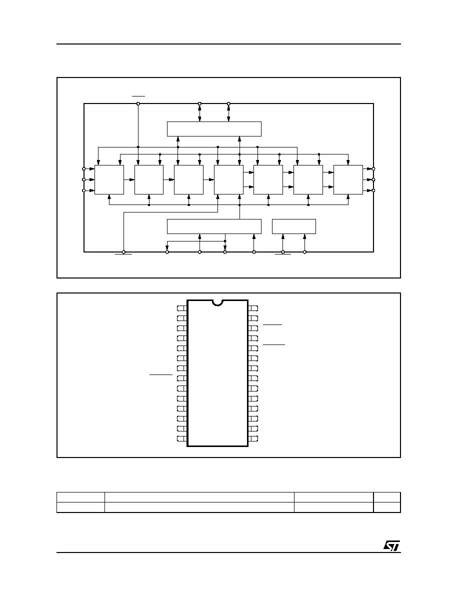
The functional STA003T chip partitioning is de-
scribed in Fig.1.
STA003T
MPEG 2.5 LAYER III AUDIO DECODER
Æ
1/32
I
2
C CONTROL
SERIAL
INPUT
INTERFACE
BUFFER
MPEG 2.5
LAYER III
DECODER
CORE
CHANNEL
CONFIG.
&
VOLUME
CONTROL
OUTPUT
BUFFER
PCM
OUTPUT
INTERFACE
PARSER
26
3
4
RESET
SDA
SCL
5
6
7
BIT_EN
SCKR
SDI
SDO
9
10
11
SCKT
LRCKT
SYSTEM & AUDIO CLOCKS
TEST INTERFACE
SRC_INT
VDD_5/CLK_OUT
XTI
XTO
OCLK
TESTEN
SCANEN
D99AU1005
8
28
21
20
12
24
25
Figure 1. BLOCK DIAGRAM: MPEG 2.5 Layer III Decoder Hardware Partitioning.
THERMAL DATA
Symbol
Parameter
Value
Unit
R
th j-amb
Thermal resistance Junction to Ambient
85
∞C/W
VDD_1
VSS_1
RESET
SDA
SCL
SCKR
SDI
BIT_EN
SDO
VDD_4
VSS_4
XTI
FILT
XTO
PVSS
PVDD
VDD_3
VSS_3
1
3
2
4
5
6
7
8
9
26
25
24
23
22
20
21
19
27
10
28
VDD_2
TESTEN
D99AU1003
VSS_2
SCKT
LRCKT
VSS_5
SRC_INT
SCANEN
11
12
13
18
16
17
15
14
OCLK
VDD_5/CLK_OUT
Figure 2. PIN CONNECTION
Fig. 2 describes the STA003T pinout in SO28 package
STA003T
2/32
PIN DESCRIPTION
Type
Pin Name
Type
Function
PAD Description
1
VDD_1
Supply Voltage
2
VSS_1
Ground
3
SDA
I/O
I
2
C Serial Data + Acknowledge
CMOS Input Pad Buffer
CMOS 4mA Output Drive
4
SCL
I
I
2
C Serial Clock
CMOS Input Pad Buffer
5
SDI
I
Receiver Serial Data
CMOS Input Pad Buffer
6
SCKR
I
Receiver Serial Clock
CMOS Input Pad Buffer
7
BIT_EN
I
Bit Enable
CMOS Input Pad Buffer with pull up
8
SRC_INT
I
Interrupt Line For S.R. Control
CMOS Input Pad Buffer
9
SDO
O
Transmitter Serial Data (PCM
Data)
CMOS 4mA Output Drive
10
SCKT
O
Transmitter Serial Clock
CMOS 4mA Output Drive
11
LRCLKT
O
Transmitter Left/Right Clock
CMOS 4mA Output Drive
12
OCLK
I/O
Oversampling Clock for DAC
CMOS Input Pad Buffer
CMOS 4mA Output Drive
13
VSS_2
Ground
14
VDD_2
Supply Voltage
15
VSS_3
Ground
16
VDD_3
Supply Voltage
17
PVDD
PLL Power
18
PVSS
PLL Ground
19
FILT
O
PLL Filter Ext. Capacitor Conn.
20
XTO
O
Crystal Output
CMOS 4mA Output Drive
21
XTI
I
Crystal Input (Clock Input)
Specific Level Input Pad (see paragraph 2.1)
22
VSS_4
Ground
23
VDD_4
Supply Voltage
24
TESTEN
I
Test Enable
CMOS Input Pad Buffer with pull up
25
SCANEN
I
Scan Enable
CMOS Input Pad Buffer
26
RESET
I
System Reset
CMOS Input Pad Buffer with pull up
27
VSS_5
Ground
28
VDD_5/CLK_OUT
Power/14.72MHz Buffered Output
Clock
CMOS 4mA Output Drive
Note: In functional mode TESTEN must be connected to VDD, SCANEN to ground.
ABSOLUTE MAXIMUM RATINGS
Symbol
Parameter
Value
Unit
V
DD
Power Supply
-0.3 to 4
V
V
i
Voltage on Input pins
-0.3 to V
DD
+0.3
V
V
O
Voltage on output pins
-0.3 to V
DD
+0.3
V
T
stg
Storage Temperature
-40 to +150
∞C
T
oper
Operative ambient temp
-20 to +85
∞C
STA003T
3/32
1. ELECTRICAL CHARACTERISTICS: V
DD
= 3.3V
±
0.3V; T
amb
= 0 to 70∞C; Rg = 50
unless otherwise
specified
DC OPERATING CONDITIONS
Symbol
Parameter
Value
V
DD
Power Supply Voltage
2.7 to 3.6V
T
j
Operating Junction Temperature
-20 to 125∞C
GENERAL INTERFACE ELECTRICAL CHARACTERISTICS
Symbol
Parameter
Test Condition
Min.
Typ.
Max.
Unit
Note
I
IL
Low Level Input Current
Without pull-up device
V
i
= 0V
-10
10
µ
A
1
I
IH
High Level Input Current
Without pull-up device
V
i
= V
DD
-10
10
µ
A
1
V
esd
Electrostatic Protection
Leakage < 1
µ
A
2000
V
2
Note 1: The leakage currents are generally very small, < 1nA. The value given here is a maximum that can occur after an electrostatic stress
on the pin.
Note 2: Human Body Model.
DC ELECTRICAL CHARACTERISTICS
Symbol
Parameter
Test Condition
Min.
Typ.
Max.
Unit
Note
V
IL
Low Level Input Voltage
0.2*V
DD
V
V
IH
High Level Input Voltage
0.8*V
DD
V
V
ol
Low Level Output Voltage
I
ol
= Xma
0.4V
V
1, 2
V
oh
High Level Output Voltage
0.85*V
DD
V
1, 2
Note 1: Takes into account 200mV voltage drop in both supply lines.
Note 2: X is the source/sink current under worst case conditions and is reflected in the name of the I/O cell according to the drive capability.
Symbol
Parameter
Test Condition
Min.
Typ.
Max.
Unit
Note
I
pu
Pull-up current
V
i
= 0V; pin numbers 7, 24
and 26
-25
-66
-125
µ
A
1
R
pu
Equivalent Pull-up
Resistance
50
k
Note 1: Min. condition: V
DD
= 2.7V, 125∞C Min process
Max. condition: V
DD
= 3.6V, -20∞C Max.
POWER DISSIPATION
Symbol
Parameter
Test Condition
Min.
Typ.
Max.
Unit
Note
PD
Power Dissipation
@ V
DD
= 3V
Sampling_freq
24 kHz
120
mW
Sampling_freq
32 kHz
125
mW
Sampling_freq
48 kHz
135
mW
STA003T
4/32
V
DD
100nF
1
2
V
DD
100nF
14
13
V
SS
V
DD
100nF
16
15
V
DD
100nF
23
22
V
SS
V
SS
V
SS
17
18
27
28
26
RESET
24
TESTEN
25
SCANEN
VDD_5/CLK_OUT
V
DD
PV
SS
PV
DD
100nF
4.7
µ
F
4.7
µ
F
PV
DD
PV
SS
V
SS
10K
1K
4.7nF
PV
SS
470pF
19
20
21
8
7
6
5
12
11
10
9
4
3
XTO
XTI
SCR_INT
BIT_EN
SCKR
SDI
OCLK
LRCKT
SCKT
SDO
SCL
SDA
D99AU1004
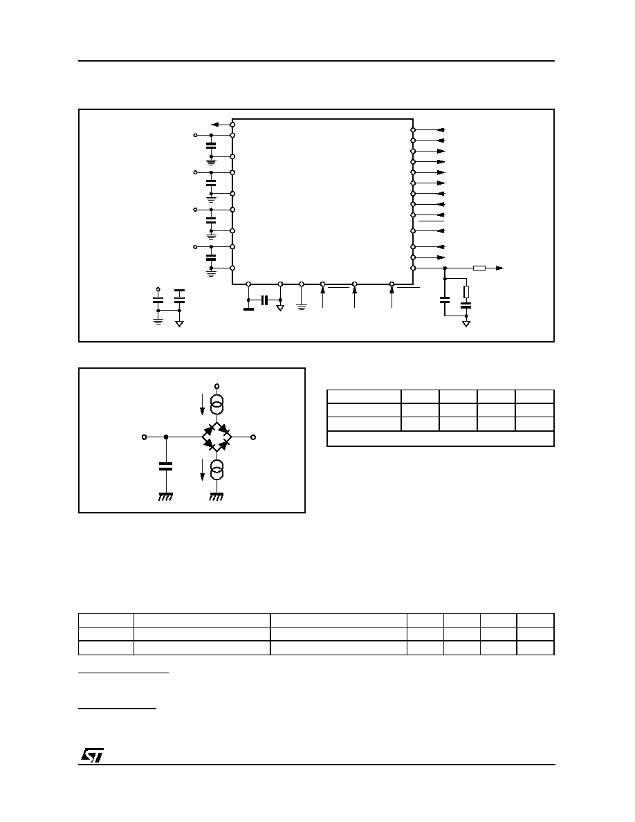
Figure 3. Test Circuit
I
OL
I
OH
C
L
V
REF
V
DD
OUTPUT
D98AU967
Test Load Circuit
Output
I
OL
I
OH
C
L
V
REF
SDA
1mA
100pF
3.6V
Other Outputs
100
µ
A
100
µ
A
100pF
1.5V
Test Load
2. FUNCTIONAL DESCRIPTION
2.1 - Clock Signal
The STA003T input clock is derivated from an ex-
ternal source or from a 14.72 MHz crystal.
XTI is an input Pad with specific levels.
Symbol
Parameter
Test Condition
Min.
Typ.
Max.
Unit
V
IL
Low Level Input Voltage
V
DD
-1.8
V
V
IH
High Level Input Voltage
V
DD
-0.8
V
CMOS compatibility
The XTI pad low and high levels are CMOS compatible; XTI pad noise margin is better than typical
CMOS pads.
TTL compatibility
The XTI pad low level is compatible with TTL while the high level is not compatible (for example if V
DD
=
3V TTL min high level = 2.0V while XTI min high level = 2.2V)
STA003T
5/32