 | –≠–ª–µ–∫—Ç—Ä–æ–Ω–Ω—ã–π –∫–æ–º–ø–æ–Ω–µ–Ω—Ç: STA013T | –°–∫–∞—á–∞—Ç—å:  PDF PDF  ZIP ZIP |
February 2004
ORDERING NUMBERS: STA013$ (SO28)
STA013T$ (TQFP44)
STA013B$ (LFBGA 8x8)
SINGLE CHIP MPEG2 LAYER 3 DECODER
SUPPORTING:
- All features specified for Layer III in ISO/IEC
11172-3 (MPEG 1 Audio)
- All features specified for Layer III in ISO/IEC
13818-3.2 (MPEG 2 Audio)
- Lower sampling frequencies syntax extension,
(not specified by ISO) called MPEG 2.5
DECODES LAYER III STEREO CHANNELS,
DUAL CHANNEL, SINGLE CHANNEL
(MONO)
SUPPORTING ALL THE MPEG 1 & 2 SAM-
PLING FREQUENCIES AND THE EXTEN-
SION TO MPEG 2.5:
48, 44.1, 32, 24, 22.05, 16, 12, 11. 025, 8 KHz
ACCEPTS MPEG 2.5 LAYER III ELEMEN-
TARY COMPRESSED BITSTREAM WITH
DATA RATE FROM 8 Kbit/s UP TO 320 Kbit/s
DIGITAL VOLUME CONTROL
DIGITAL BASS & TREBLE CONTROL
SERIAL BITSTREAM INPUT INTERFACE
ANCILLARY DATA EXTRACTION VIA I2C IN-
TERFACE.
SERIAL PCM OUTPUT INTERFACE (I
2
S
AND OTHER FORMATS)
PLL FOR INTERNAL CLOCK AND FOR OUT-
PUT PCM CLOCK GENERATION
LOW POWER CONSUMPTION:
85mW AT 2.4V
CRC CHECK AND SYNCHRONISATION ER-
ROR DETECTION WITH SOFTWARE INDI-
CATORS
I
2
C CONTROL BUS
LOW POWER 3.3V CMOS TECHNOLOGY
10 MHz, 14.31818 MHz, OR 14.7456 MHz
EXTERNAL INPUT CLOCK OR BUILT-IN IN-
DUSTRY STANDARD XTAL OSCILLATOR
DIFFERENT FREQUENCIES MAY BE SUP-
PORTED UPON REQUEST TO STM
APPLICATIONS
PC SOUND CARDS
MULTIMEDIA PLAYERS
DESCRIPTION
The STA013 is a fully integrated high flexibility
MPEG Layer III Audio Decoder, capable of de-
coding Layer III compressed elementary streams,
as specified in MPEG 1 and MPEG 2 ISO stand-
ards. The device decodes also elementary streams
compressed by using low sampling rates, as speci-
fied by MPEG 2.5.
STA013 receives the input data through a Serial
Input Interface. The decoded signal is a stereo,
mono, or dual channel digital output that can be
sent directly to a D/A converter, by the PCM Out-
put Interface. This interface is software program-
mable to adapt the STA013 digital output to the
most common DACs architectures used on the
market.
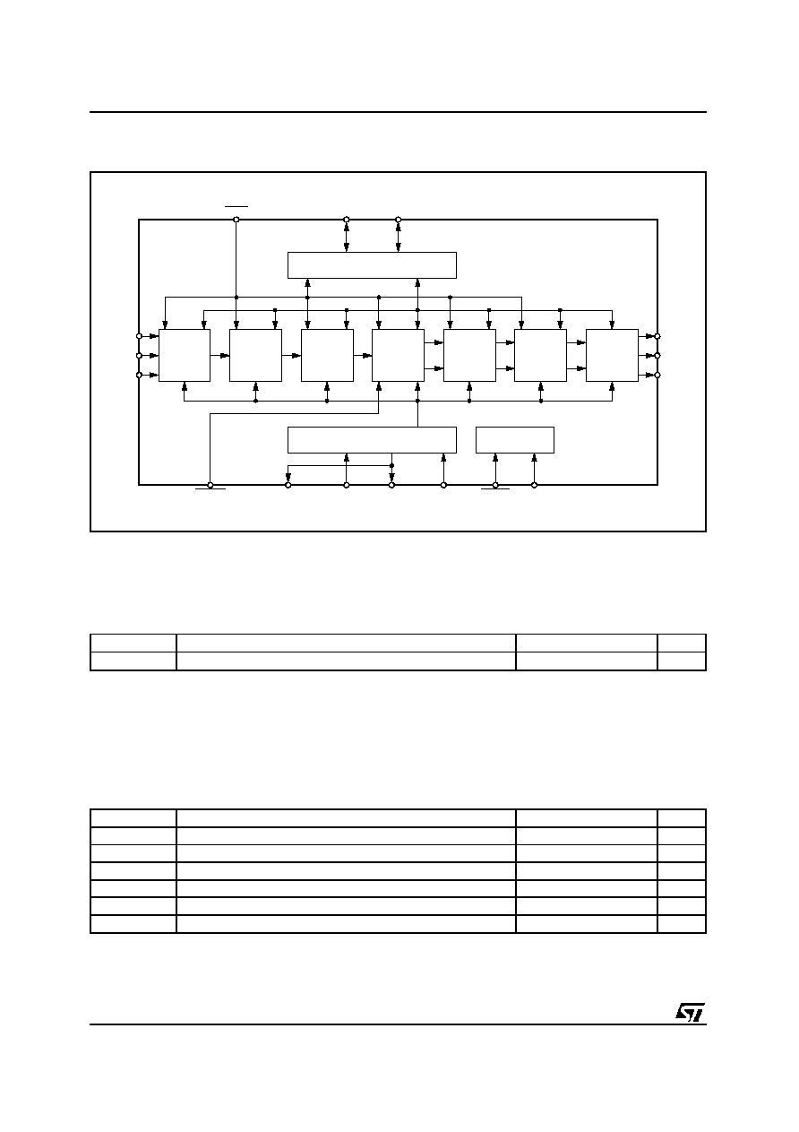
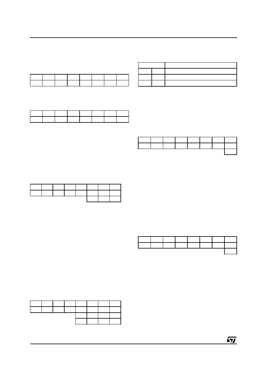
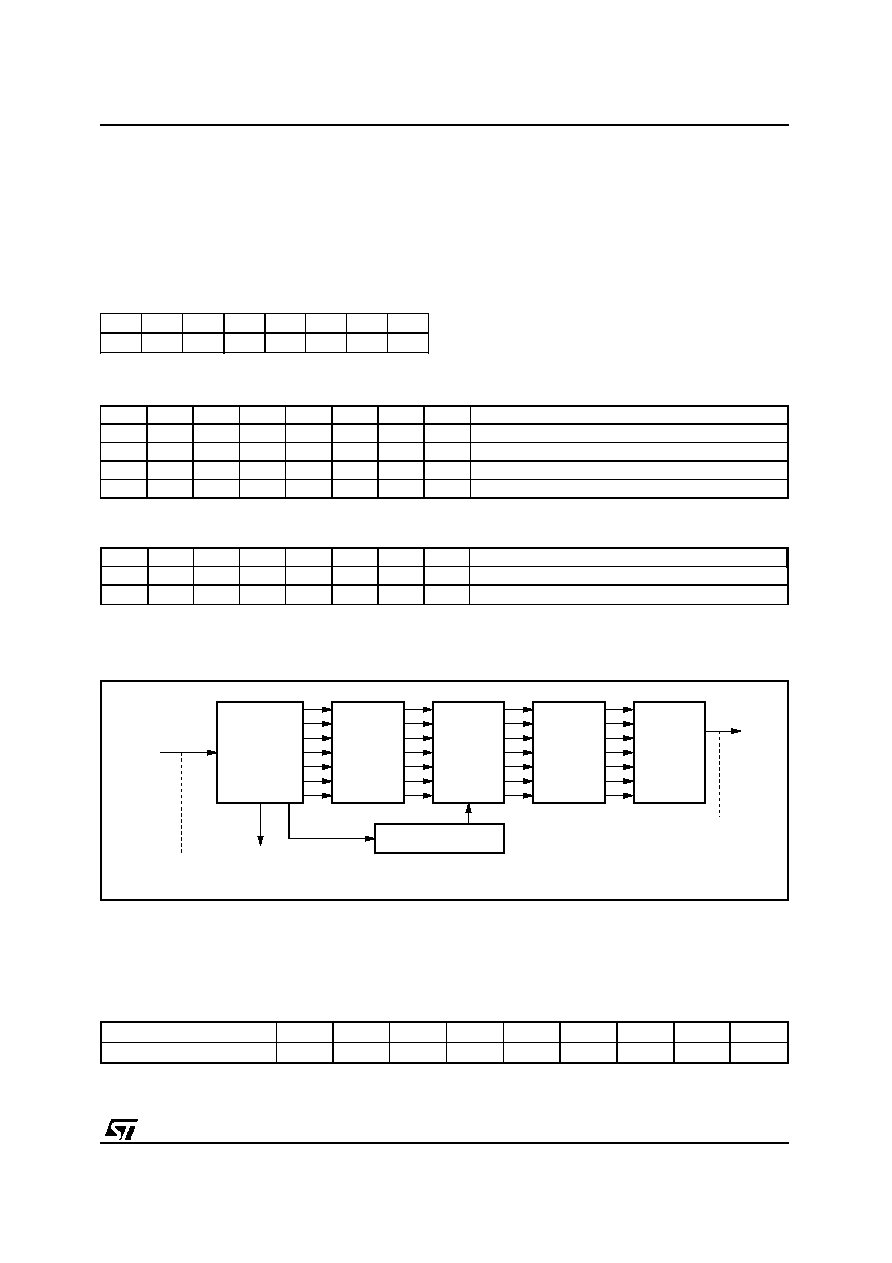
The functional STA013 chip partitioning is de-
scribed in Fig.1.
STA013
STA013B STA013T
MPEG 2.5 LAYER III AUDIO DECODER
Æ
SO28
TQFP44
LFBGA64
1/38
I
2
C CONTROL
SERIAL
INPUT
INTERFACE
BUFFER
MPEG 2.5
LAYER III
DECODER
CORE
CHANNEL
CONFIG.
&
VOLUME
CONTROL
OUTPUT
BUFFER
PCM
OUTPUT
INTERFACE
PARSER
26
3
4
RESET
SDA
SCL
5
6
7
BIT_EN
SCKR
SDI
SDO
9
10
11
SCKT
LRCKT
SYSTEM & AUDIO CLOCKS
TEST INTERFACE
SRC_INT
OUT_CLK/DATA_REQ
XTI
XTO
OCLK
TESTEN
SCANEN
D98AU965
8
28
21
20
12
24
25
Figure 1. Block Diagram: MPEG 2.5 Layer III Decoder Hardware Partitioning.
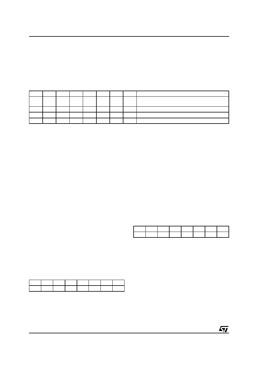
THERMAL DATA
Symbol
Parameter
Value
Unit
R
th j-amb
Thermal resistance Junction to Ambient
85
∞C/W
ABSOLUTE MAXIMUM RATINGS
Symbol
Parameter
Value
Unit
V
DD
Power Supply
-0.3 to 4
V
V
i
Voltage on Input pins
-0.3 to V
DD
+0.3
V
V
O
Voltage on output pins
-0.3 to V
DD
+0.3
V
T
stg
Storage Temperature
-40 to +150
∞C
T
oper
Operative ambient temp
-40 to +85 (*)
∞C
T
j
Operating Junction Temperature
-40 to 125
∞C
(*) guaranteed by design.
STA013 - STA013B - STA013T
2/38
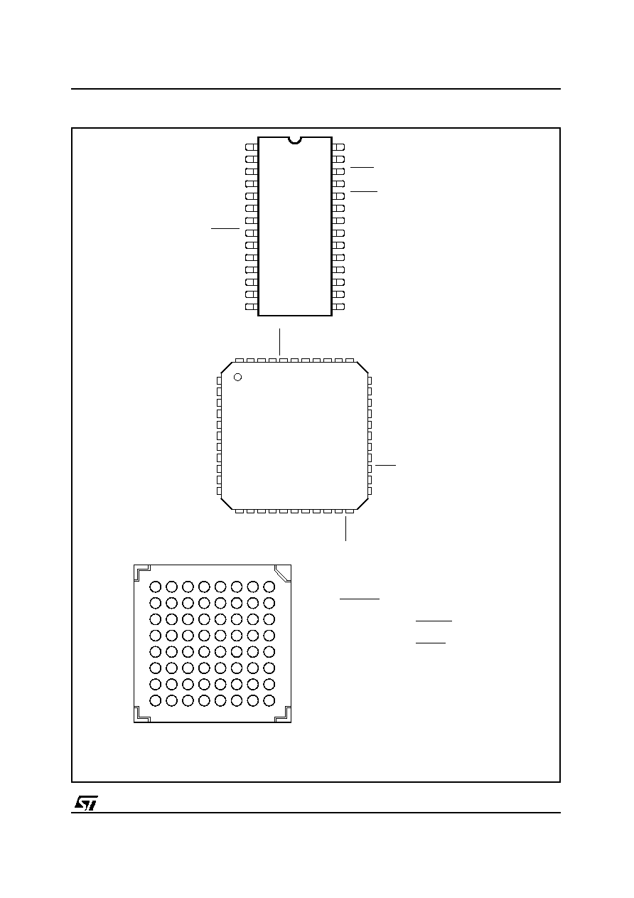
Figure 2. Pin Connection
VDD_1
VSS_1
RESET
SDA
SCL
SCKR
SDI
BIT_EN
SDO
VDD_4
VSS_4
XTI
FILT
XTO
PVSS
PVDD
VDD_3
VSS_3
1
3
2
4
5
6
7
8
9
26
25
24
23
22
20
21
19
27
10
28
VDD_2
TESTEN
D98AU911A
VSS_2
SCKT
LRCKT
VSS_5
SRC_INT
SCANEN
11
12
13
18
16
17
15
14
OCLK
OUT_CLK/DATA_REQ
1
2
3
5
6
4
7
8
9
10
17
11
18
19
20
21
22
44
43
42
41
39
40
38
37
36
35
34
28
27
26
24
23
25
33
32
31
29
30
N.C.
LRCKT
OCLK
N.C.
VSS_2
VDD_2
VSS_3
VDD_3
N.C.
PVDD
PVSS
FILT
XTO
N.C.
XTI
N.C.
N.C.
N.C.
VSS_4
N.C.
VDD_4
TESTEN
SDI
N.C.
SCKR
N.C.
BIT_EN
N.C.
SRC_INT
N.C.
SDO
N.C.
SCKT
N.C.
SCANEN
RESET
VSS_5
OUT_CLK/DATA_REC
N.C.
VDD_1
VSS_1
SDA
SCL
N.C.
D99AU1019
12
13
14
15
16
SO28
TQFP44
A
A1 = SDI
B2 = SCKR
D4 = BIT_EN
D1 = SRC_INT
E2 = SDO
F2 = SCKT
H1 = LRCKT
H3 = OCLK
F3 = VSS_2
E4 = VDD_2
G4 = VSS_3
G5 = VDD_3
F5 = PVDD
G6 = PVSS
1
2
3
4
5
6
7
8
B
C
D
E
F
G
H
D99AU1085
G7 = FILT
G8 = XTO
F7 = XTI
E7 = VSS4
C8 = VDD4
D7 = TESTEN
A7 = SCANEN
B6 = RESET
A5 = VSS5
C5 = OUT_CLK/DATA_REQ
B5 = VDD1
B4 = VSS1
A4 = SDA
B3 = SCL
LFBGA64
STA013 - STA013B - STA013T
3/38
PIN DESCRIPTION
SO28
TQFP44
LFBGA64
Pin Name
Type
Function
PAD Description
1
29
B5
VDD_1
Supply Voltage
2
30
B4
VSS_1
Ground
3
31
A4
SDA
I/O
i
2
C Serial Data + Acknowledge
CMOS Input Pad Buffer
CMOS 4mA Output Drive
4
32
B3
SCL
I
I
2
C Serial Clock
CMOS Input Pad Buffer
5
34
A1
SDI
I
Receiver Serial Data
CMOS Input Pad Buffer
6
36
B2
SCKR
I
Receiver Serial Clock
CMOS Input Pad Buffer
7
38
D4
BIT_EN
I
Bit Enable
CMOS Input Pad Buffer
with pull up
8
40
D1
SRC_INT
I
Interrupt Line For S.R. Control
CMOS Input Pad Buffer
9
42
E2
SDO
O
Transmitter Serial Data (PCM
Data)
CMOS 4mA Output Drive
10
44
F2
SCKT
O
Transmitter Serial Clock
CMOS 4mA Output Drive
11
2
H1
LRCKT
O
Transmitter Left/Right Clock
CMOS 4mA Output Drive
12
3
H3
OCLK
I/O
Oversampling Clock for DAC
CMOS Input Pad Buffer
CMOS 4mA Output Drive
13
5
F3
VSS_2
Ground
14
6
E4
VDD_2
Supply Voltage
15
7
G4
VSS_3
Ground
16
8
G5
VDD_3
Supply Voltage
17
10
F5
PVDD
PLL Power
18
11
G6
PVSS
PLL Ground
19
12
G7
FILT
O
PLL Filter Ext. Capacitor Conn.
20
13
G8
XTO
O
Crystal Output
CMOS 4mA Output Drive
21
15
F7
XTI
I
Crystal Input (Clock Input)
Specific Level Input Pad
(see paragraph 2.1)
22
19
E7
VSS_4
Ground
23
21
C8
VDD_4
Supply Voltage
24
22
D7
TESTEN
I
Test Enable
CMOS Input Pad Buffer
with pull up
25
24
A7
SCANEN
I
Scan Enable
CMOS Input Pad Buffer
26
25
B6
RESET
I
System Reset
CMOS Input Pad Buffer
with pull up
27
26
A5
VSS_5
Ground
28
27
C5
OUT_CLK/
DATA_REQ
O
Buffered Output Clock/
Data Request Signal
CMOS 4mA Output Drive
Note: SRC_INT signal is used by STA013 internal software in Broadcast Mode only; in Multimedia mode SRC_INT must be connected to
V
DD
In functional mode TESTEN must be connected to VDD, SCANEN to ground.
STA013 - STA013B - STA013T
4/38
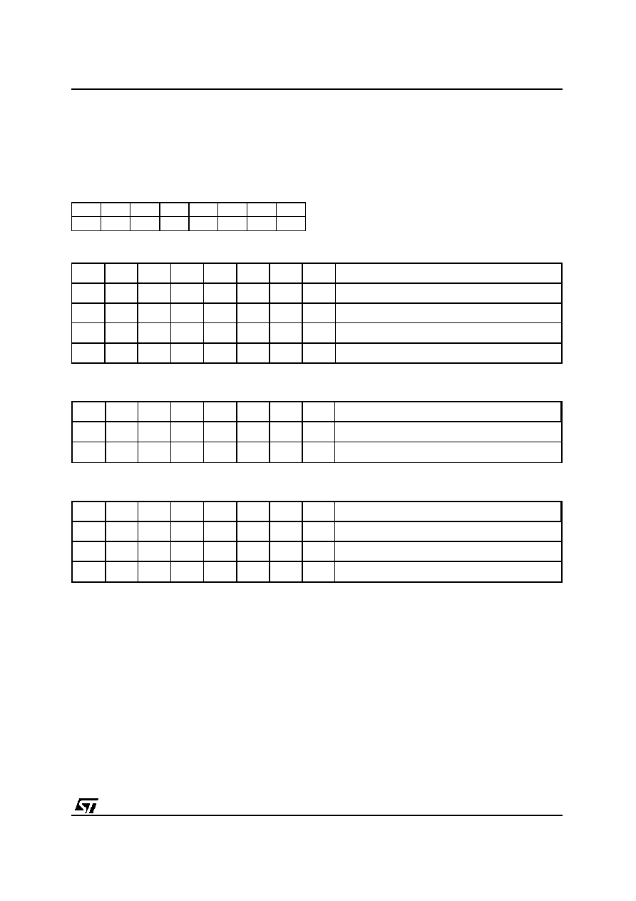
1. ELECTRICAL CHARACTERISTICS: V
DD
= 2.7V
±
0.3V; T
amb
= 0 to 70∞C; Rg = 50
unless otherwise
specified
DC OPERATING CONDITIONS
Symbol
Parameter
Value
V
DD
Power Supply Voltage
2.4 to 3.6V
GENERAL INTERFACE ELECTRICAL CHARACTERISTICS
Symbol
Parameter
Test Condition
Min.
Typ.
Max.
Unit
Note
I
IL
Low Level Input Current
Without pull-up device
V
i
= 0V
-10
10
µ
A
1
I
IH
High Level Input Current
Without pull-up device
V
i
= V
DD
= 3.6V
-10
10
µ
A
1
V
esd
Electrostatic Protection
Leakage < 1
µ
A
2000
V
2
Note 1: The leakage currents are generally very small, < 1nA. The value given here is a maximum that can occur after an electrostatic stress
on the pin.
Note 2: Human Body Model.
DC ELECTRICAL CHARACTERISTICS
Symbol
Parameter
Test Condition
Min.
Typ.
Max.
Unit
Note
V
IL
Low Level Input Voltage
0.2*V
DD
V
V
IH
High Level Input Voltage
0.8*V
DD
V
V
ol
Low Level Output Voltage
I
ol
= Xma
0.4V
V
1, 2
V
oh
High Level Output Voltage
0.85*V
DD
V
1, 2
Note 1: Takes into account 200mV voltage drop in both supply lines.
Note 2: X is the source/sink current under worst case conditions and is reflected in the name of the I/O cell according to the drive capability.
Symbol
Parameter
Test Condition
Min.
Typ.
Max.
Unit
Note
I
pu
Pull-up current
V
i
= 0V; pin numbers 7, 24
and 26; V
DD
= 3V
-25
-66
-125
µ
A
1
R
pu
Equivalent Pull-up
Resistance
50
k
Note 1: Min. condition: V
DD
= 2.4V, 125∞C Min process
Max. condition: V
DD
= 3.6V, -20∞C Max.
POWER DISSIPATION
Symbol
Parameter
Test Condition
Min.
Typ.
Max.
Unit
Note
PD
Power Dissipation
@ V
DD
= 3V
Sampling_freq
24 kHz
76
mW
Sampling_freq
32 kHz
79
mW
Sampling_freq
48 kHz
85
mW
STA013 - STA013B - STA013T
5/38
V
DD
100nF
1
2
V
DD
100nF
14
13
V
SS
V
DD
100nF
16
15
V
DD
100nF
23
22
V
SS
V
SS
V
SS
17
18
27
28
26
RESET
24
TESTEN
25
SCANEN
OUT_CLK/DATA_REQ
V
DD
PV
SS
PV
DD
100nF
4.7
µ
F
4.7
µ
F
PV
DD
PV
SS
V
SS
10K
1K
4.7nF
PV
SS
470pF
19
20
21
8
7
6
5
12
11
10
9
4
3
XTO
XTI
SCR_INT
BIT_EN
SCKR
SDI
OCLK
LRCKT
SCKT
SDO
SCL
SDA
D98AU966
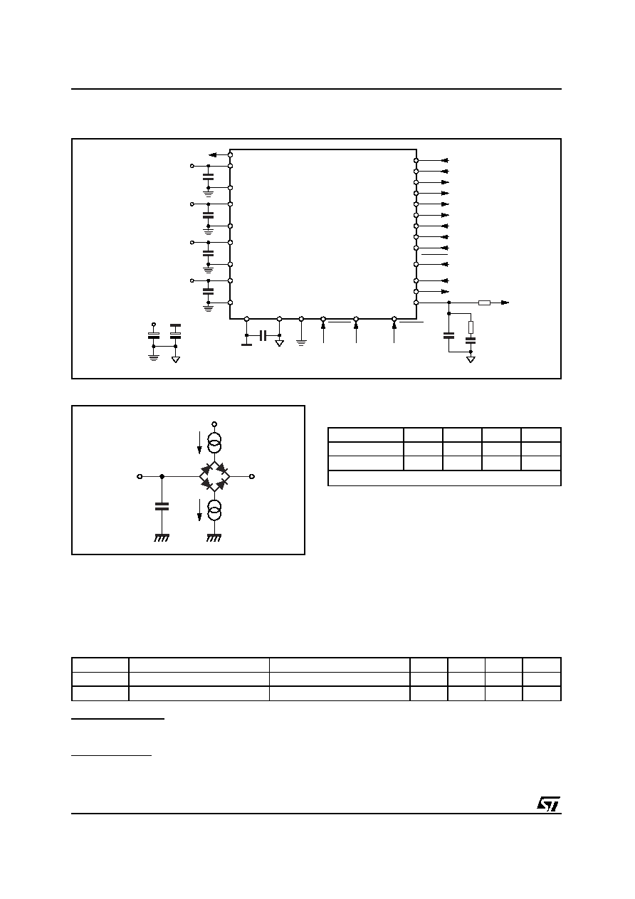
Figure 3. Test Circuit
I
OL
I
OH
C
L
V
REF
V
DD
OUTPUT
D98AU967
Figure 4. Test Load Circuit
Output
I
OL
I
OH
C
L
V
REF
SDA
1mA
100pF
3.6V
Other Outputs
100
µ
A
100
µ
A
100pF
1.5V
Test Load
2. FUNCTIONAL DESCRIPTION
2.1 - Clock Signal
The STA013 input clock is derivated from an ex-
ternal source or from a industry standard crystal
oscillator, generating input frequencies of 10,
14.31818 or 14.7456 MHz.
Other frequencies may be supported upon re-
quest to STMicroelectronics. Each frequency is
supported by downloading a specific configura-
tion file, provided by STM
XTI is an input Pad with specific levels.
Symbol
Parameter
Test Condition
Min.
Typ.
Max.
Unit
V
IL
Low Level Input Voltage
V
DD
-1.8
V
V
IH
High Level Input Voltage
V
DD
-0.8
V
CMOS compatibility
The XTI pad low and high levels are CMOS compatible; XTI pad noise margin is better than typical
CMOS pads.
TTL compatibility
The XTI pad low level is compatible with TTL while the high level is not compatible (for example if V
DD
=
3V TTL min high level = 2.0V while XTI min high level = 2.2V)
STA013 - STA013B - STA013T
6/38
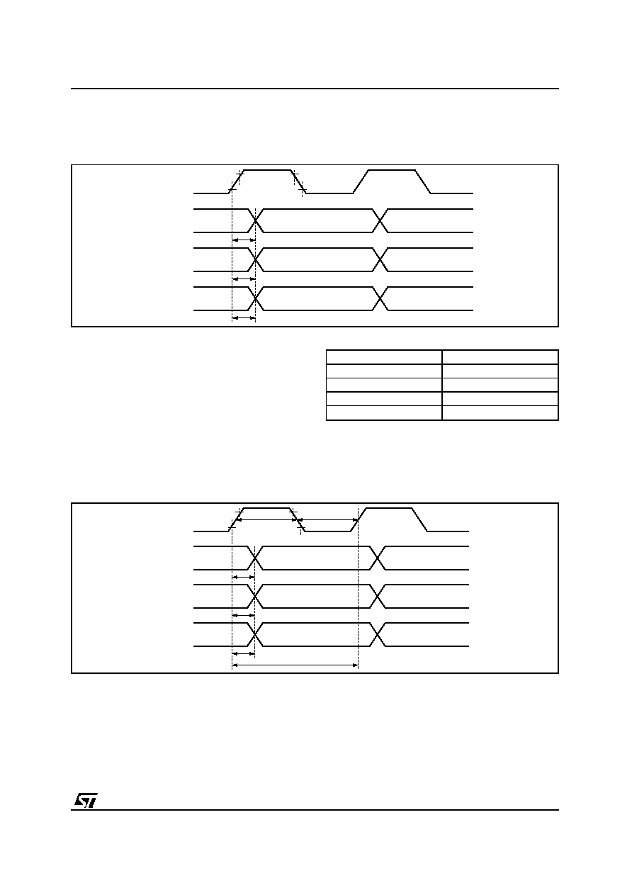
SCLK_POL=0
SCLK_POL=4
DATA IGNORED
DATA VALID
SCKR
SCKR
SDI
BIT_EN
D98AU968A
DATA IGNORED
Figure 6. Serial Input Interface Clocks
DATA
SOURCE
µ
P
MPEG
DECODER
IIC
D98AU912
IIC
SDO
SCKT
LRCKT
SERIAL AUDIO INTERFACE
SDI
SCKR
BIT_EN
XTO
DAC
RX
TX
XTI
FILT
PLL
OCLK
SCL
SDA
DATA_REQ
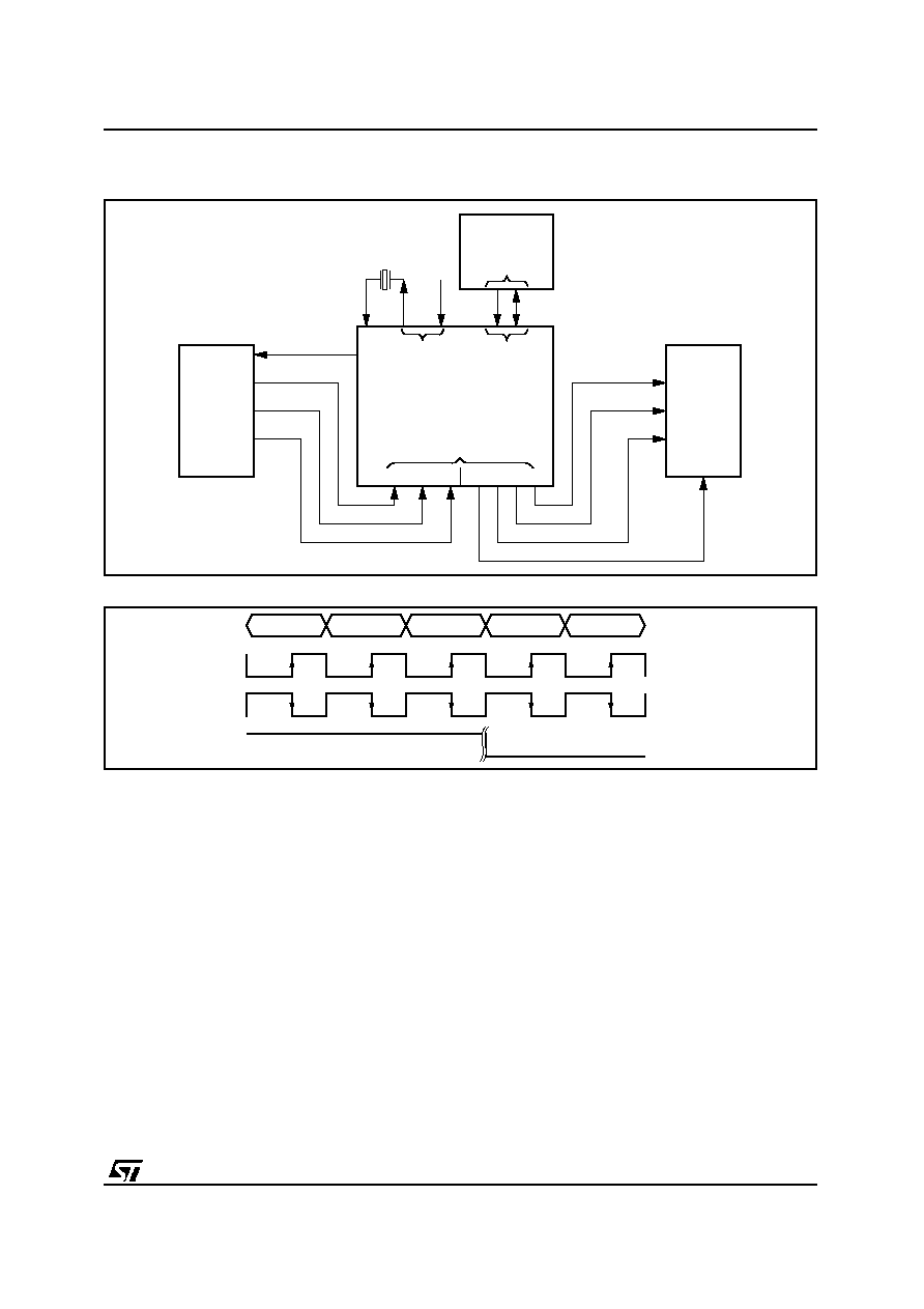
Figure 5. MPEG Decoder Interfaces.
2.2 - Serial Input Interface
STA013 receives the input data (MSB first)
thought the Serial Input Interface (Fig.5). It is a
serial communication interface connected to the
SDI (Serial Data Input) and SCKR (Receiver Se-
rial Clock).
The interface can be configured to receive data
sampled on both rising and falling edge of the
SCKR clock.
The BIT_EN pin, when set to low, forces the bit-
stream input interface to ignore the incoming
data. For proper operation Bit-E
N
line shold be
toggled only when SCR is stable low (for both
SCLK_POL configuration) The possible configu-
rations are described in Fig. 6.
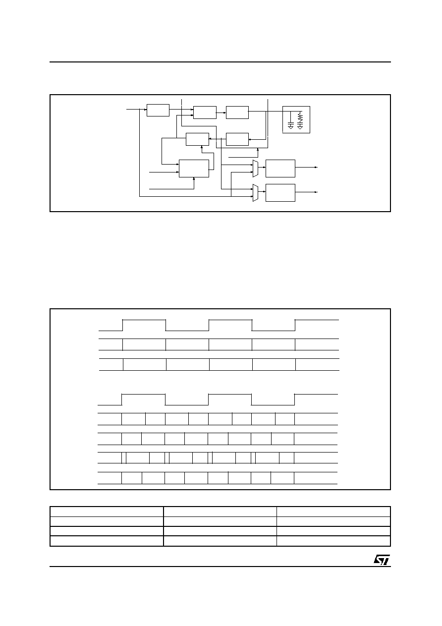
2.3 - PLL & Clock Generator System
When STA013 receives the input clock, as de-
scribed in Section 2.1, and a valid layer III input
bit stream, the internal PLL locks, providing to the
DSP Core the master clock (DCLK), and to the
Audio Output Interface the nominal frequencies of
the incoming compressed bit stream. The STA013
PLL block diagram is described in Figure 7.
The audio sample rates are obtained dividing the
oversampling clock (OCLK) by software program-
mable factors. The operation is done by STA013
embedded software and it is transparent to the
user.
The STA013 PLL can drive directly most of the
commercial DACs families, providing an over
sampling clock, OCLK, obtained dividing the VCO
frequency with a software programmable dividers.
STA013 - STA013B - STA013T
7/38
R
C
C
XTI2DSPCLK
XTI2OCLK
X
S
N
M
PFD
CP
VCO
Switching
Circuit
OCLK
DCLK
Update FRAC
FRAC
XTI
Disable PLL
Figure 7. PLL and Clocks Generation System
2.4 - PCM Output Interface
The decoded audio data are output in serial PCM
format. The interface consists of the following sig-
nals:
SDO PCM Serial Data Output
SCKT PCM Serial Clock Output
LRCLK Left/Right Channel Selection Clock
The output samples precision is selectable from
16 to 24 bits/word, by setting the output precision
with PCMCONF (16, 18, 20 and 24 bits mode)
register. Data can be output either with the most
significant bit first (MS) or least significant bit first
(LS), selected by writing into a flag of the
PCMCONF register.
Figure 8 gives a description of the several
STA013 PCM Output Formats.
The sample rates set decoded by STA013 is de-
scribed in Table 1.
LRCKT
SDO
SDO
PCM_FORMAT = 0
PCM_DIFF = 0
PCM_FORMAT = 1
PCM_DIFF = 1
32 SCLK Cycles
32 SCLK Cycles
32 SCLK Cycles
32 SCLK Cycles
32 SCLK Cycles
M
S
M
S
L
S
L
S
L
S
L
S
M
S
M
S
M
S
L
S
M
S
L
S
L
S
L
S
M
S
M
S
LRCKT
SDO
SDO
PCM_ORD = 1
PCM_PREC is 16 bit mode
PCM_ORD = 0
PCM_PREC is 16 bit mode
16 SCLK Cycles
16 SCLK Cycles
16 SCLK Cycles
16 SCLK Cycles
16 SCLK Cycles
M
S
M
S
L
S
L
S
L
S
L
S
M
S
M
S
M
S
L
S
M
S
L
S
L
S
L
S
M
S
M
S
SDO
PCM_FORMAT = 0
PCM_DIFF = 1
L
S
L
S
M
S
M
S
M
S
L
S
L
S
M
S
SDO
PCM_FORMAT = 1
PCM_DIFF = 1
L
S
L
S
M
S
M
S
M
S
L
S
L
S
M
S
0
0
0
0
0
0
0
0
0
0
0
0
0
0
0
0
MSB
MSB
MSB
MSB
Figure 8. PCM Output Formats
Table 1: MPEG Sampling Rates (KHz)
MPEG 1
MPEG 2
MPEG 2.5
48
24
12
44.1
22.05
11.025
32
16
8
STA013 - STA013B - STA013T
8/38
2.5 - STA013 Operation Mode
The STA013 can work in two different modes,
called Multimedia Mode and Broadcast Mode.
In Multimedia Mode, STA013 decodes the in-
coming bitstream, acting as a master of the data
communication from the source to itself.
This control is done by a specific buffer manage-
ment, controlled by STA013 embedded software.
The data source, by monitoring the DATA_REQ
line, send to STA013 the input data, when the
signal is high (default configuration).
The communication is stopped when the
DATA_REQ line is low.
In this mode the fractional part of the PLL is dis-
abled and the audio clocks are generated at
nominal rates. Fig. 9 describes the default
DATA_REQ signal behaviour.
Programming STA013 it is possible to invert the
polarity of the DATA_REQ line (register
REQ_POL).
In Broadcast Mode, STA013 works receiving a
bitstream with the input speed regulated by the
source. In this configuration the source has to
guarantee that the bitrate is equivalent to the
nominal bitrate of the decoded stream.
To compensate the difference between the nomi-
nal and the real sampling rates, the STA013 em-
bedded software controls the fractional PLL op-
eration. Portable or Mobile applications need
normally to operate in Broadcast Mode. In both
modes the MPEG Synchronisation is automatic
and transparent to the user. To operate in Multi-
media mode, the STA013, pin nr. 8, SCR-INT
must be connected to VDD on the application
board.
2.6 - STA013 Decoding States
There are three different decoder states: Idle,
Init, and Decode. Commands to change the de-
coding states are described in the STA013 I
2
C
registers description.
Idle Mode
In this mode the decoder is waiting for the RUN
command. This mode should be used to initialise
the configuration register of the device. The DAC
connected to STA013 can be initialised during
this mode (set MUTE to 1).
PLAY
MUTE
Clock State
PCM Output
X
0
Not Running
0
X
1
Running
0
Init Mode
"PLAY" and "MUTE" changes are ignored in this
mode. The internal state of the decoder will be
updated only when the decoder changes from the
state "init" to the state "decode". The "init" phase
ends when the first decoded samples are at the
output stage of the device.
Decode Mode
This mode is completely described by the follow-
ing table:
PLAY
MUTE
Clock State
PCM
Output
Decoding
0
0
Not Running
0
No
0
1
Running
0
No
1
0
Running
Decoded
Samples
Yes
1
1
Running
0
Yes
3 - I
2
C BUS SPECIFICATION
The STA013 supports the I
2
C protocol. This pro-
tocol defines any device that sends data on to the
bus as a transmitter and any device that reads
the data as a receiver. The device that controls
the data transfer is known as the master and the
others as the slave. The master always starts the
transfer and provides the serial clock for synchro-
nisation. The STA013 is always a slave device in
all its communications.
3. 1 - COMMUNICATION PROTOCOL
3.1.0 - Data transition or change
Data changes on the SDA line must only occur
when the SCL clock is low. SDA transition while
the clock is high are used to identify START or
STOP condition.
3.1.1 - Start condition
START is identified by a high to low transition of
the data bus SDA signal while the clock signal
SCL is stable in the high state.
A START condition must precede any command
for data transfer.
SOURCE SEND DATA TO STA013
DATA_REQ
SOURCE STOPS TRANSMITTING DATA
SOURCE STOPS TRANSMITTING DATA
D98AU913
Figure 9.
STA013 - STA013B - STA013T
9/38
3.1.2 - Stop condition
STOP is identified by low to high transition of the
data bus SDA signal while the clock signal SCL is
stable in the high state. A STOP condition termi-
nates communications between STA013 and the
bus master.
3.1.3 - Acknowledge bit
An acknowledge bit is used to indicate a success-
ful data transfer. The bus transmitter, either mas-
ter or slave, releases the SDA bus after sending
8 bit of data.
During the 9th clock pulse the receiver pulls the
SDA bus low to acknowledge the receipt of 8 bits
of data.
3.1.4 - Data input
During the data input the STA013 samples the
SDA signal on the rising edge of the clock SCL.
For correct device operation the SDA signal has
to be stable during the rising edge of the clock
and the data can change only when the SCL line
is low.
3.2 - DEVICE ADDRESSING
To start communication between the master and
the STA013, the master must initiate with a start
condition. Following this, the master sends onto
the SDA line 8 bits (MSB first) corresponding to
the device select address and read or write
mode.
The 7 most significant bits are the device address
identifier, corresponding to the I
2
C bus definition.
For the STA013 these are fixed as 1000011.
The 8th bit (LSB) is the read or write operation
RW, this bit is set to 1 in read mode and 0 for
write mode. After a START condition the STA013
identifies on the bus the device address and, if a
match is found, it acknowledges the identification
on SDA bus during the 9th bit time. The following
byte after the device identification byte is the in-
ternal space address.
3.3 - WRITE OPERATION (see fig. 10)
Following a START condition the master sends a
device select code with the RW bit set to 0.
The STA013 acknowledges this and waits for the
byte of internal address.
After receiving the internal bytes address the
STA013 again responds with an acknowledge.
3.3.1 - Byte write
In the byte write mode the master sends one data
byte, this is acknowledged by STA013. The mas-
ter then terminates the transfer by generating a
STOP condition.
3.3.2 - Multibyte write
The multibyte write mode can start from any inter-
nal address. The transfer is terminated by the
master generating a STOP condition.
DEV-ADDR
ACK
START
D98AU826A
RW
DATA
NO ACK
STOP
CURRENT
ADDRESS
READ
DEV-ADDR
ACK
START
RW
SUB-ADDR
ACK
DEV-ADDR
ACK
STOP
RANDOM
ADDRESS
READ
DATA
NO ACK
START
RW
DEV-ADDR
ACK
START
DATA
ACK
DATA
ACK
STOP
SEQUENTIAL
CURRENT
READ
DATA
NO ACK
DEV-ADDR
ACK
START
RW
SUB-ADDR
ACK
DEV-ADDR
ACK
SEQUENTIAL
RANDOM
READ
DATA
ACK
START
RW
DATA
ACK
NO ACK
STOP
DATA
RW=
HIGH
Figure 11. Read Mode Sequence
DEV-ADDR
ACK
START
D98AU825B
RW
SUB-ADDR
ACK
DATA IN
ACK
STOP
BYTE
WRITE
DEV-ADDR
ACK
START
RW
SUB-ADDR
ACK
DATA IN
ACK
STOP
MULTIBYTE
WRITE
DATA IN
ACK
Figure 10. Write Mode Sequence
STA013 - STA013B - STA013T
10/38
3.4 - READ OPERATION (see Fig. 11)
3.4.1 - Current byte address read
The STA013 has an internal byte address
counter. Each time a byte is written or read, this
counter is incremented.
For the current byte address read mode, follow-
ing a START condition the master sends the de-
vice address with the RW bit set to 1.
The STA013 acknowledges this and outputs the
byte addressed by the internal byte address
counter. The master does not acknowledge the
received byte, but terminates the transfer with a
STOP condition.
3.4.2 - Sequential address read
This mode can be initiated with either a current
address read or a random address read. How-
ever in this case the master does acknowledge
the data byte output and the STA013 continues to
output the next byte in sequence.
To terminate the streams of bytes the master
does not acknowledge the last received byte, but
terminates the transfer with a STOP condition.
The output data stream is from consecutive byte
addresses, with the internal byte address counter
automatically incremented after one byte output.
4 - I
2
C REGISTERS
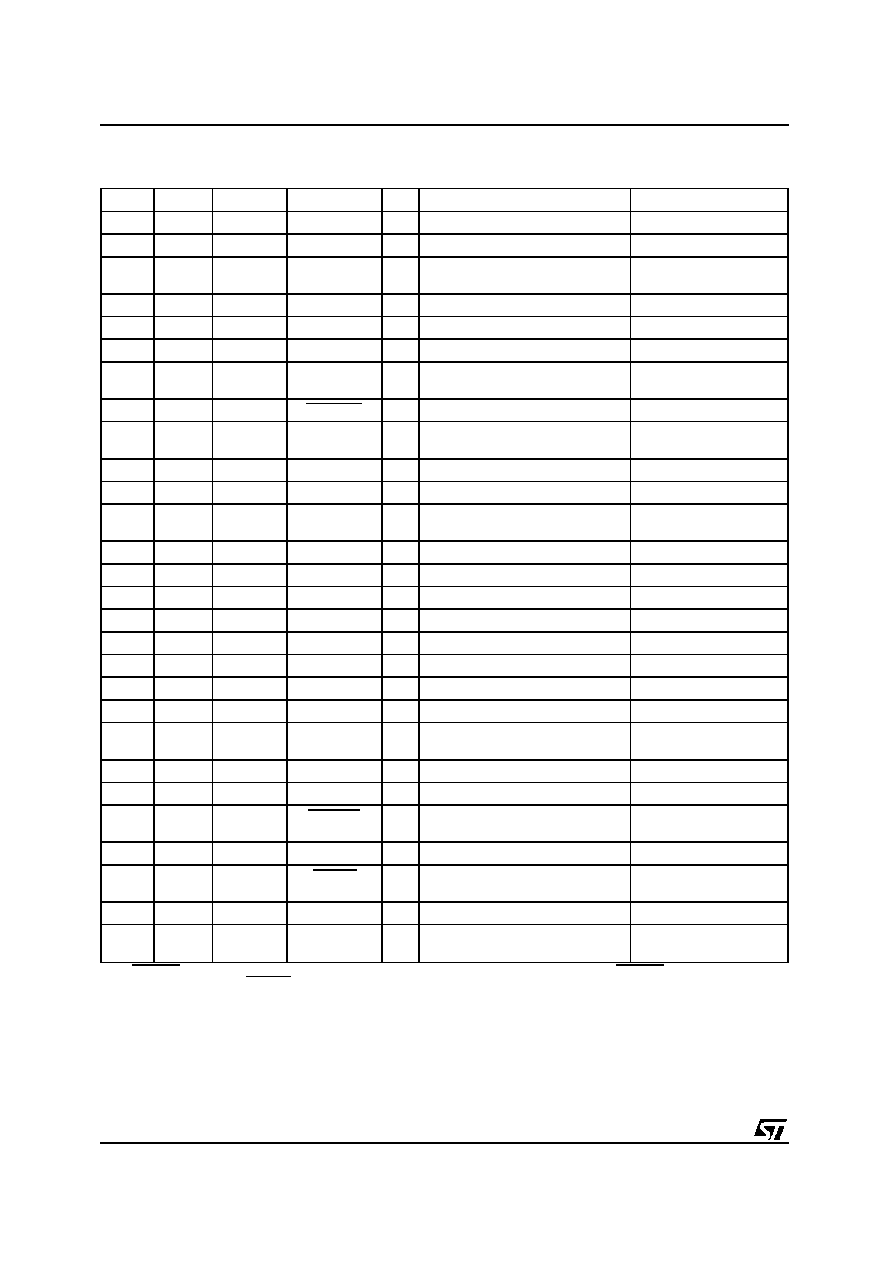
The following table gives a description of the
MPEG Source Decoder (STA013) register list.
The first column (HEX_COD) is the hexadecimal
code for the sub-address.
The second column (DEC_COD) is the decimal
code.
The third column (DESCRIPTION) is the descrip-
tion of the information contained in the register.
The fourth column (RESET) inidicate the reset
value if any. When no reset value is specifyed,
the default is "undefined".
The fifth column (R/W) is the flag to distinguish
register "read only" and "read and write", and the
useful size of the register itself.
Each register is 8 bit wide. The master shall oper-
ate reading or writing on 8 bits only.
I
2
C REGISTERS
HEX_COD
DEC_COD
DESCRIPTION
RESET
R/W
$00
0
VERSION
R (8)
$01
1
IDENT
0xAC
R (8)
$05
5
PLLCTL [7:0]
0xA1
R/W (8)
$06
6
PLLCTL [20:16] (MF[4:0]=M)
0x0C
R/W (8)
$07
7
PLLCTL [15:12] (IDF[3:0]=N)
0x00
R/W (8)
$0B
11
reserved
$0C
12
REQ_POL
0x01
R/W (8)
$0D
13
SCLK_POL
0x04
R/W (8)
$0F
15
ERROR_CODE
0x00
R (8)
$10
16
SOFT_RESET
0x00
W (8)
$13
19
PLAY
0x01
R/W(8)
$14
20
MUTE
0x00
R/W(8)
$16
22
CMD_INTERRUPT
0x00
R/W(8)
$18
24
DATA_REQ_ENABLE
0x00
R/W(8)
$40
64
SYNCSTATUS
0x00
R (8)
$41
65
ANCCOUNT_L
0x00
R (8)
$42
66
ANCCOUNT_H
0x00
R (8)
STA013 - STA013B - STA013T
11/38
I
2
C REGISTERS (continued)
HEX_COD
DEC_COD
DESCRIPTION
RESET
R/W
$43
67
HEAD_H[23:16]
0x00
R(8)
$44
68
HEAD_M[15:8]
0x00
R(8)
$45
69
HEAD_L[7:0]
0x00
R(8)
$46
70
DLA
0x00
R/W (8)
$47
71
DLB
0xFF
R/W (8)
$48
72
DRA
0x00
R/W (8)
$49
73
DRB
0xFF
R/W (8)
$50
80
MFSDF_441
0x00
R/W (8)
$51
81
PLLFRAC_441_L
0x00
R/W (8)
$52
82
PLLFRAC_441_H
0x00
R/W (8)
$54
84
PCM DIVIDER
0x03
R/W (8)
$55
85
PCMCONF
0x21
R/W (8)
$56
86
PCMCROSS
0x00
R/W (8)
$59
89
ANC_DATA_1 [7:0]
0x00
R (8)
$5A
90
ANC_DATA_2 [15:8]
0x00
R (8)
$5B
91
ANC_DATA_3 [23:16]
0x00
R (8)
$5C
92
ANC_DATA_4 [31:24]
0x00
R (8)
$5D
93
ANC_DATA_5 [39:32]
0x00
R (8)
$61
97
MFSDF (X)
0x07
R/W (8)
$63
99
DAC_CLK_MODE
0x00
R/W (8)
$64
100
PLLFRAC_L
0x46
R/W (8)
$65
101
PLLFRAC_H
0x5B
R/W (8)
$67
103
FRAME_CNT_L
0x00
R (8)
$68
104
FRAME_CNT_M
0x00
R (8)
$69
105
FRAME_CNT_H
0x00
R (8)
$6A
106
AVERAGE_BITRATE
0x00
R (8)
$71
113
SOFTVERSION
R (8)
$72
114
RUN
0x00
R/W (8)
$77
119
TREBLE_FREQUENCY_LOW
0x00
R/W (8)
$78
120
TREBLE_FREQUENCY_HIGH
0x00
R/W (8)
$79
121
BASS_FREQUENCY_LOW
0x00
R/W (8)
$7A
122
BASS_FREQUENCY_HIGH
0x00
R/W (8)
$7B
123
TREBLE_ENHANCE
0x00
R/W (8)
$7C
124
BASS_ENHANCE
0x00
R/W (8)
$7D
125
TONE_ATTEN
0x00
R/W (8)
Note:
1) The HEX_COD is the hexadecimal adress that the microcontroller has to generate to access the information.
2) RESERVED: register used for production test only, or for future use.
STA013 - STA013B - STA013T
12/38

4.1 - STA013 REGISTERS DESCRIPTION
The STA013 device includes 128 I
2
C registers. In
this document, only the user-oriented registers
are described. The undocumented registers are
reserved. These registers must never be ac-
cessed (in Read or in Write mode). The Read-
Only registers must never be written.
The following table describes the meaning of the
abbreviations used in the I
2
C registers descrip-
tion:
Symbol
Comment
NA
Not Applicable
UND
Undefined
NC
No Charge
RO
Read Only
WO
Write Only
R/W
Read and Write
R/WS
Read, Write in specific mode
VERSION
Address: 0x00
Type: RO
MSB
LSB
b7
b6
b5
b4
b3
b2
b1
b0
V8
V7
V6
V5
V4
V3
V2
V1
The VERSION register is read-only and it is used
to identify the IC on the application board.
IDENT
Address: 0x01
Type: RO
Software Reset: 0xAC
Hardware Reset: 0xAC
MSB
LSB
b7
b6
b5
b4
b3
b2
b1
b0
1
0
1
0
1
1
0
0
IDENT is a read-only register and is used to iden-
tify the IC on an application board. IDENT always
has the value "0xAC"
PLLCTL
Address: 0x05
Type: R/W
Software Reset: 0x21
Hardware Reset: 0x21
MSB
LSB
b7
b6
b5
b4
b3
b2
b1
b0
XTO_
BUF
XTOD
IS
OCLK
EN
SYS2O
CLK
PPLD
IS
XTI2DS
PCLK
XTI2O
CLK
UPD_F
RAC
UPD_FRAC: when is set to 1, update FRAC in
the switching circuit. It is set to 1 after autoboot.
XTI2OCLK: when is set to 1, use the XTI as input
of the divider X instead of VCO output. It is set to
0 on HW reset.
XTI2DSPCLK: when is to 1, set use the XTI as in-
put of the divider S instead of VCO output. It is
set to 0 on HW reset.
PLLDIS: when set to 1, the VCO output is dis-
abled. It is set to 0 on HW reset.
SYS2OCLK: when is set to 1, the OCLK fre-
quency is equal to the system frequency. It is
useful for testing. It is set to 0 on HW reset.
OCLKEN: when is set to 1, the OCLK pad is en-
able as output pad. It is set to 1 on HW reset.
XTODIS: when is set to 1, the XTO pad is dis-
able. It is set to 0 on HW reset.
XTO_BUF: when this bit is set, the pin nr. 28
(OUT_CLOCK/DATA_REQ) is enabled. It is set
to 0 after autoboot.
PLLCTL (M)
Address: 0x06
Type: R/W
Software Reset: 0x0C
Hardware Reset: 0x0C
PLLCTL (N)
Address: 0x07
Type: R/W
Software Reset: 0x00
Hardware Reset: 0x00
The M and N registers are used to configure the
STA013 PLL by DSP embedded software.
M and N registers are R/W type but they are
completely controlled, on STA013, by DSP soft-
ware.
REQ_POL
Address: 0x0C
Type: R/W
Software Reset: 0x01
Hardware Reset: 0x00
STA013 - STA013B - STA013T
13/38
Hardware Reset: 0x01
The REQ_POL registers is used to program the
polarity of the DATA_REQ line.
MSB
LSB
b7
b6
b5
b4
b3
b2
b1
b0
0
0
0
0
0
0
0
1
Default polarity (the source sends data when the
DATA_REQ line is high)
MSB
LSB
b7
b6
b5
b4
b3
b2
b1
b0
0
0
0
0
0
1
0
1
Inverted polarity (the source sends data when the
DATA_REQ line is low)
SCKL_POL
Address: 0x0D
Type: R/W
Software Reset: 0x04
Hardware Reset: 0x04
MSB
LSB
b7
b6
b5
b4
b3
b2
b1
b0
X
X
X
X
X
0
0
0
(1)
1
0
0
(2)
X = don't care
SCKL_POL is used to select the working polarity
of the Input Serial Clock (SCKR).
(1) If SCKL_POL is set to 0x00, the data (SDI)
are sent with the falling edge of SCKR
and sampled on the rising edge.
(2) If SCKL_POL is set to 0x04, the data (SDI)
are sent with the rising edge of SCKR and
sampled on the falling edge.
ERROR_CODE
Address: 0x0F
Type: RO
Software Reset: 0x00
Hardware Reset: 0x00
MSB
LSB
b7
b6
b5
b4
b3
b2
b1
b0
X
X
X
X
0
0
0
0
(1)
0
0
0
1
(2)
0
0
1
0
(3)
X = don't care
ERROR_CODE register contains the last error
occourred if any. The codes can be as follows:
Code
Description
(1)
0x00
No error since the last SW or HW Reset
(2)
0x01
CRC Failure
(3)
0x02
DATA not available
SOFT_RESET
Address: 0x10
Type: WO
Software Reset: 0x00
Hardware Reset: 0x00
MSB
LSB
b7
b6
b5
b4
b3
b2
b1
b0
X
X
X
X
X
X
X
0
1
X = don't care; 0 = normal operation; 1 = reset
When this register is written, a soft reset occours.
The STA013 core command register and the in-
terrupt register are cleared. The decoder goes in
to idle mode.
PLAY
Address: 0x13
Type: R/W
Software Reset: 0x01
Hardware Reset: 0x01
MSB
LSB
b7
b6
b5
b4
b3
b2
b1
b0
X
X
X
X
X
X
X
0
1
X = don't care; 0 = normal operation; 1 = play
The PLAY command is handled according to the
state of the decoder, as described in section 2.5.
PLAY only becomes active when the decoder is
in DECODE mode.
STA013 - STA013B - STA013T
14/38
DATA_REQ_ENABLE
Address: 0x18
Type: R/W
Software Reset: 0x00
Hardware Reset: 0x00
MSB
LSB
b7
b6
b5
b4
b3
b2
b1
b0
Description
X
X
X
X
X
0
X
X
buffered output clock
X
X
X
X
X
1
X
X
request signal
MUTE
Address: 0x14
Type: R/W
Software Reset: 0x00
Hardware Reset: 0x00
MSB
LSB
b7
b6
b5
b4
b3
b2
b1
b0
X
X
X
X
X
X
X
0
1
X = don't care; 0 = normal operation; 1 = mute
The MUTE command is handled according to the
state of the decoder, as described in section 2.5.
MUTE sets the clock running.
CMD_INTERRUPT
Address: 0x16
Type: R/W
Software Reset: 0x00
Hardware Reset: 0x00
MSB
LSB
b7
b6
b5
b4
b3
b2
b1
b0
X
X
X
X
X
X
X
0
1
X = don't care;
0 = normal operation;
1 = write into I
2
C/Ancillary Data
The INTERRUPT is used to give STA013 the
command to write into the I2C/Ancillary Data
Buffer (Registers: 0x59 ... 0x5D). Every time the
Master has to extract the new buffer content (5
bytes) it writes into this register, setting it to a
non-zero value.
SYNCSTATUS
Address: 0x40
Type: RO
Software Reset: 0x00
Hardware Reset: 0x00
MSB
LSB
b7
b6
b5
b4
b3
b2
b1
b0
Description
X
X
X
X
X
X
SS1
SS0
0
0
Research of sync word
0
1
Wait for Confirmation
1
0
Synchronised
1
1
not used
The DATA_REQ_ENABLE register is used to
configure Pin n. 28 working as buffered output
clock or data request signal, used for multimedia
mode.
The buffered Output Clock has the same fre-
quency than the input clock (XTI)
STA013 - STA013B - STA013T
15/38
ANCCOUNT_L
Address: 0x41
Type: RO
Software Reset: 0x00
Hardware Reset: 0x00
MSB
LSB
b7
b6
b5
b4
b3
b2
b1
b0
AC7
AC6
AC5
AC4
AC3
AC2
AC1
AC0
ANCCOUNT_H
Address: 0x42
Type: RO
Software Reset: 0x00
Hardware Reset: 0x00
ANCCOUNT_H
MSB
LSB
b7
b6
b5
b4
b3
b2
b1
b0
AC15 AC14 AC13 AC12 AC11 AC10
AC9
AC8
ANCCOUNT registers are logically concatenated
and indicate the number of Ancillary Data bits
available at every correctly decoded MPEG
frame.
HEAD_H[23:16]
MSB
LSB
b7
b6
b5
b4
b3
b2
b1
b0
X
X
X
H20
H19
H18
H17
H16
x = don't care
HEAD_M[15:8]
MSB
LSB
b7
b6
b5
b4
b3
b2
b1
b0
H15
H14
H13
H12
H1`1
H10
H9
H8
HEAD_L[7:0]
MSB
LSB
b7
b6
b5
b4
b3
b2
b1
b0
H7
H6
H5
H4
H3
H2
H1
H0
Address: 0x43, 0x44, 0x45
Type: RO
Software Reset: 0x00
Hardware Reset: 0x00
Head[1:0] emphasis
Head[2] original/copy
Head[3] copyrightHead
[5:4] mode extension
Head[7:6] mode
Head[8] private bit
Head[9] padding bit
Head[11:10] sampling frequency index
Head[15:12] bitrate index
Head[16] protection bit
Head[18:17] layer
Head[19] ID
Head[20] ID_ex
The HEAD registers can be viewed as logically
concatenated to store the MPEG Layer III Header
content. The set of three registers is updated
every time the synchronisation to the new MPEG
frame is achieved
STA013 - STA013B - STA013T
16/38
The meaning of the flags are shown in the follow-
ing tables:
MPEG IDs
IDex
ID
0
0
MPEG 2.5
0
1
reserved
1
0
MPEG 2
1
1
MPEG 1
Layer
in Layer III these two flags must be set always to
"01".
Protection_bit
It equals "1" if no redundancy has been added
and "0" if redundancy has been added.
Bitrate_index
indicates the bitrate (Kbit/sec) depending on the
MPEG ID.
bitrate index
ID = 1
ID = 0
'0000'
free
free
'0001'
32
8
'0010'
40
16
'0011'
48
24
'0100'
56
32
'0101'
64
40
'0110'
80
48
'0111'
96
56
'1000'
112
64
'1001'
128
80
'1010'
160
96
'1011'
192
112
'1100'
224
128
'1101'
256
144
'1110'
320
160
'1111'
forbidden
forbidden
Sampling Frequency
indicates the sampling frequency of the encoded
audio signal (KHz) depending on the MPEG ID
Sampling
Frequency
MPEG1
MPEG2
MPEG2.5
'00'
44.1
22.05
11.03
'01'
48
24
12
'10'
32
16
8
'11'
reserved
reserved
reserved
Padding bit
if this bit equals '1', the frame contains an addi-
tional slot to adjust the mean bitrate to the sam-
pling frequency, otherwise this bit is set to '0'.
Private bit
Bit for private use. This bit will not be used in the
future by ISO/IEC.
Mode
Indicates the mode according to the following ta-
ble. The joint stereo mode is intensity_stereo
and/or ms_stereo.
mode
mode specified
'00'
stereo
'01'
joint stereo (intensity_stereo and/or ms_stereo)
'10'
dual_channel
'11'
single_channel (mono)
Mode extension
These bits are used in joint stereo mode. They in-
dicates which type of joint stereo coding method
is applied. The frequency ranges, over which the
intensity_stereo and ms_stereo modes are ap-
plied, are implicit in the algorithm.
Copyright
If this bit is equal to '0', there is no copyright on
the bitstream, '1' means copyright protected.
Original/Copy
This bit equals '0' if the bitstream is a copy, '1' if it
is original.
Emphasis
Indicates the type of de-emphasis that shall be
used.
emphasis
emphasis specified
'00'
none
'01'
50/15 microseconds
'10'
reserved
'11'
CCITT J,17
STA013 - STA013B - STA013T
17/38
DLA register is used to attenuate the level of
audio output at the Left Channel using the butter-
fly shown in Fig. 12. When the register is set to
255 (0xFF), the maximum attenuation is
achieved.
A decimal unit correspond to an attenuation step
of 1 dB.
DLA
Address: 0x46
Type: R/W
Software Reset: 0x00
Hardware Reset: 0x00
MSB
LSB
b7
b6
b5
b4
b3
b2
b1
b0
Description
DLA7
DLA6
DLA5
DLA4
DLA3
DLA2
DLA1
DLA0
OUTPUT ATTENUATION
0
0
0
0
0
0
0
0
NO ATTENUATION
0
0
0
0
0
0
0
1
-1dB
0
0
0
0
0
0
1
0
-2dB
:
:
:
:
:
:
:
:
:
0
1
1
0
0
0
0
0
-96dB
DLB
Address: 0x47
Type: R/W
Software Reset: 0xFF
Hardware Reset: 0xFF
MSB
LSB
b7
b6
b5
b4
b3
b2
b1
b0
Description
DLB7
DLB6
DLB5
DLB4
DLB3
DLB2
DLB1
DLB0
OUTPUT ATTENUATION
0
0
0
0
0
0
0
0
NO ATTENUATION
0
0
0
0
0
0
0
1
-1dB
0
0
0
0
0
0
1
0
-2dB
:
:
:
:
:
:
:
:
:
0
1
1
0
0
0
0
0
-96dB
DLB register is used to re-direct the Left Channel
on the Right, or to mix both the Channels.
Default value is 0x00, corresponding at the maxi-
mum attenuation in the re-direction channel.
X
DLA
+
X
Output Left Channel
DSP Left Channel
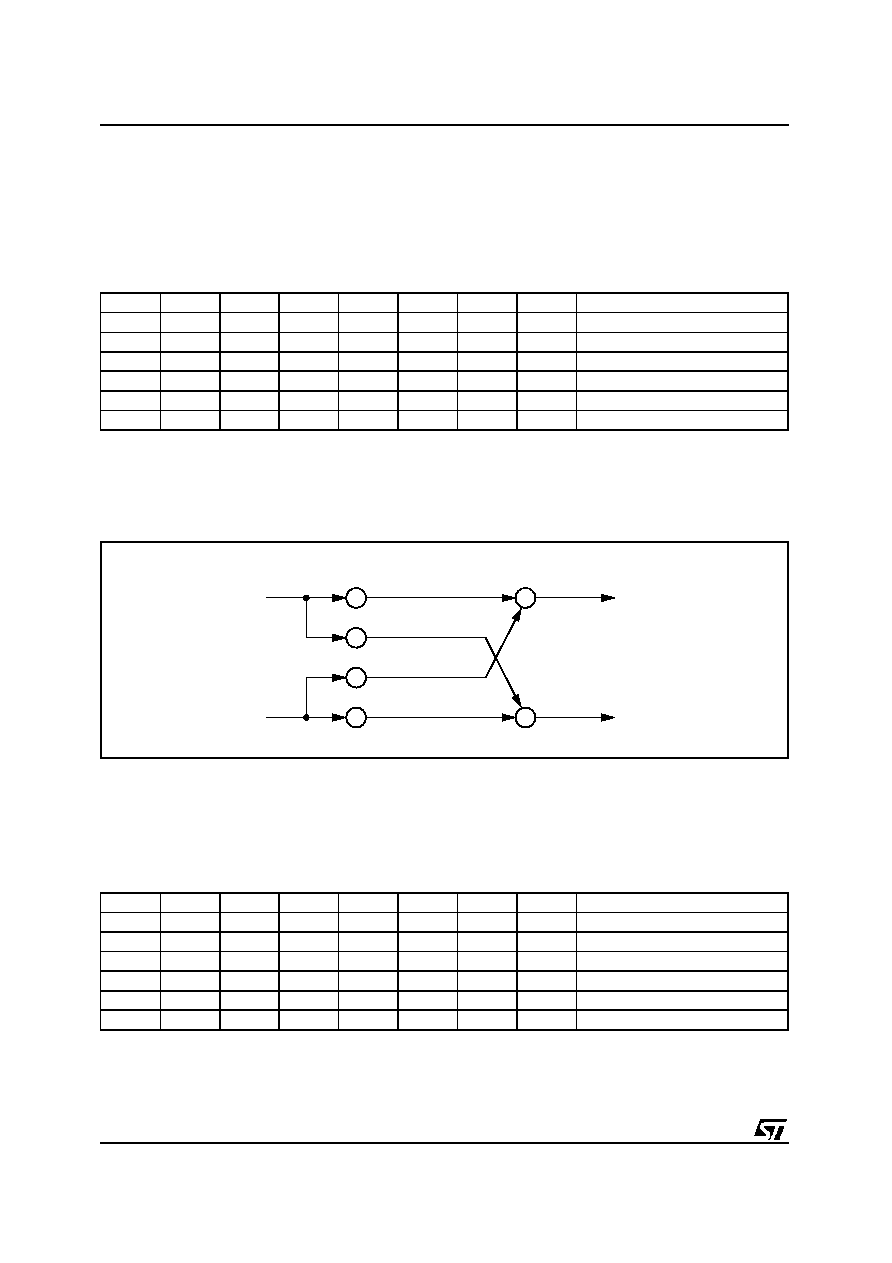
DLB
X
DRA
+
X
Output Right Channel
DSP Right Channel
DRB
D97AU667
Figure 12. Volume Control and Output Setup
STA013 - STA013B - STA013T
18/38
DRA
Address: 0x48
Type: R/W
Software Reset: 0X00
Hardware Reset: 0X00
MSB
LSB
b7
b6
b5
b4
b3
b2
b1
b0
Description
DRA7
DRA6
DRA5
DRA4
DRA3
DRA2
DRA1
DRA0
OUTPUT ATTENUATION
0
0
0
0
0
0
0
0
NO ATTENUATION
0
0
0
0
0
0
0
1
-1dB
0
0
0
0
0
0
1
0
-2dB
:
:
:
:
:
:
:
:
:
0
1
1
0
0
0
0
0
-96dB
DRA register is used to attenuate the level of
audio output at the Right Channel using the but-
terfly shown in Fig. 11. When the register is set to
255 (0xFF), the maximum attenuation is
achieved.
A decimal unit correspond to an attenuation step
of 1 dB.
DRB
Address: 0x49
Type: R/W
Software Reset: 0xFF
Hardware Reset: 0xFF
MSB
LSB
b7
b6
b5
b4
b3
b2
b1
b0
Description
DRB7
DRB6
DRB5
DRB4
DRB3
DRB2
DRB1
DRB0
OUTPUT ATTENUATION
0
0
0
0
0
0
0
0
NO ATTENUATION
0
0
0
0
0
0
0
1
-1dB
0
0
0
0
0
0
1
0
-2dB
:
:
:
:
:
:
:
:
:
0
1
1
0
0
0
0
0
-96dB
DRB register is used to re-direct the Right Chan-
nel on the Left, or to mix both the Channels.
Default value is 0x00, corresponding at the maxi-
mum attenuation in the re-direction channel.
MFSDF_441
Address: 0x50
Type: R/W
Software Reset: 0x00
Hardware Reset: 0x00
MSB
LSB
b7
b6
b5
b4
b3
b2
b1
b0
X
X
X
M4
M3
M2
M1
M0
This register contains the value for the PLL X
driver for the 44.1KHz reference frequency.
The VCO output frequency, when decoding
44.1KHz bitstream, is divided by (MFSDF_441 +1)
PLLFRAC_441_L
Address: 0x51
Type: R/W
Software Reset: 0x00
Hardware Reset: 0x00
MSB
LSB
b7
b6
b5
b4
b3
b2
b1
b0
PF7
PF6
PF5
PF4
PF3
PF2
PF1
PF0
STA013 - STA013B - STA013T
19/38
PLLFRAC_441_H
Address: 0x52
Type: R/W
Software Reset: 0x00
Hardware Reset: 0x00
MSB
LSB
b7
b6
b5
b4
b3
b2
b1
b0
PF15 PF14 PF13 PF12 PF11 PF10
PF9
PF8
The registers are considered logically concate-
nated and contain the fractional values for the
PLL, for 44.1KHz reference frequency.
(see also PLLFRAC_L and PLLFRAC_H regis-
ters)
PCMDIVIDER
Address: 0x54
Type: RW
Software Reset: 0x03
Hardware Reset: 0x03
7
6
5
4
3
2
1
0
PD7
PD6
PD5
PD4
PD3
PD2
PD1
PD0
PCMDIVIDER is used to set the frequency ratio
between the OCLK (Oversampling Clock for
DACs), and the SCKT (Serial Audio Transmitter
Clock).
The relation is the following:
SCKT_freq
=
OCLK_freq
2
(
1
+
PCM_DIV
)
The Oversampling Factor (O_FAC) is related to OCLK and SCKT by the following expression:
1) OCLK_freq = O_FAC * LRCKT_ Freq
(DAC relation)
2) OCLK_ Freq = 2 * (1+PCM_DIV) * 32*
LRCKT_Freq (when 16 bit PCM mode is used)
3) OCLK_ Freq = 2 * (1+PCM_DIV) * 64*
LRCKT_Freq (when 32 bit PCM mode is used)
4) PCM_DIV = (O_FAC/64) - 1 in 16 bit mode
5) PCM_DIV = (O_FAC/128) - 1 in 32 bit mode
Example for setting:
MSB
LSB
b7
b6
b5
b4
b3
b2
b1
b0
Description
PD7
PD6
PD5
PD4
PD3
PD2
PD1
PD0
0
0
0
0
0
1
1
1
16 bit mode
512 x Fs
0
0
0
0
0
1
0
1
16 bit mode
384 x Fs
0
0
0
0
0
0
1
1
16 bit mode
256 x Fs
0
0
0
0
0
0
1
1
32 bit mode
512 x Fs
0
0
0
0
0
0
1
0
32 bit mode
384 x Fs
0
0
0
0
0
0
0
1
32 bit mode
256 x Fs
for 16 bit PCM Mode
O_FAC = 512 ; PCM_DIV = 7
O_FAC = 256 ; PCM_DIV = 3
O_FAC = 384 ; PCM_DIV = 5
for 32 bit PCM Mode
O_FAC = 512 ; PCM_DIV = 3
O_FAC = 256 ; PCM_DIV = 1
O_FAC = 384 ; PCM_DIV = 2
STA013 - STA013B - STA013T
20/38
PCMCONF
Address: 0x55
Type: R/W
Software Reset: 0x21
Hardware Reset: 0x21
MSB
LSB
b7
b6
b5
b4
b3
b2
b1
b0
Description
X
ORD
DIF
INV
FOR
SCL
PREC (1) PREC (1)
X
1
PCM order the LS bit is transmitted First
X
0
PCM order the MS bit is transmitted First
X
0
The word is right padded
X
1
The word is left padded
X
1
LRCKT Polarity compliant to I2S format
X
0
LRCKT Polarity inverted
X
0
I2S format
X
1
Different formats
X
1
Data are sent on the rising edge of SCKT
X
0
Data are sent on the falling edge of SCKT
X
0
0
16 bit mode (16 slots transmitted)
X
0
1
18 bit mode (18 slots transmitted)
X
1
0
20 bit mode (20 slots transmitted)
X
1
1
24 bit mode (24 slots transmitted)
PCMCONF is used to set the PCM Output Inter-
face configuration:
ORD: PCM order. If this bit is set to'1', the LS Bit
is transmitted first, otherwise MS Bit is transmiited
first.
DIF: PCM_DIFF. It is used to select the position
of the valid data into the transmitted word. This
setting is significant only in 18/20/24 bit/word
mode.If it is set to '0' the word is right-padded,
otherwise it is left-padded.
INV (fig.13): It is used to select the LRCKT clock
polarity. If it is set to '1' the polarity is compliant to
I2S format (low -> left , high -> right), otherwise
the LRCKT is inverted. The default value is '0'. (if
I2S have to be selected, must be set to '1' in the
STA013 configuration phase).
FOR: FORMAT is used to select the PCM Output
Interface format.
After hw and sw reset the value is set to 0 corre-
sponding to I
2
S format.
SCL (fig.14): used to select the Transmitter Serial
Clock polarity. If set to '1' the data are sent on the
rising edge of SCKT and sampled on the falling. If
set to '0' , the data are sent on the falling edge
and sampled on the rising. This last option is the
most commonly used by the commercial DACs.
The default configuration for this flag is '0'.
PREC [1:0]: PCM PRECISION
It is used to select the PCM samples precision, as
follows:
'00': 16 bit mode (16 slots transmitted)
'01': 18 bit mode (32 slots transmitted)
'10': 20 bit mode (32 slots transmitted)
'11': 24 bit mode (32 slots transmitted)
The PCM samples precision in STA013 can be
16 or 18-20-24 bits.
When STA013 operates in 16 (18-20-24) bits
mode, the number of bits transmitted during a
LRCLT period is 32 (64).
LRCKT
LRCKT
INV_LRCLK=0
left
left
right
right
left
left
INV_LRCLK=1
Figure 13. LRCKT Polarity Selection
INV_SCLK=0
SCKT
SDO
Figure 14. SCKT Polarity Selection
INV_SCLK=1
SCKT
SDO
STA013 - STA013B - STA013T
21/38
PCMCROSS
Address: 0x56
Type: R/W
Software Reset: 0x00
Hardware Reset: 0x00
MSB
LSB
b7
b6
b5
b4
b3
b2
b1
b0
Description
X
X
X
X
X
X
0
0
Left channel is mapped on the left output.
Right channel is mapped on the Right output
X
X
X
X
X
X
0
1
Left channel is duplicated on both Output channels.
X
X
X
X
X
X
1
0
Right channel is duplicated on both Output channels
X
X
X
X
X
X
1
1
Right and Left channels are toggled
The default configuration for this register is '0x00'.
ANCILLARY DATA BUFFER
Address: 0x59 - 0x5D
Type: RO
Software Reset: 0x00
Hardware Reset: 0x00
STA013 can extract max 56 bytes/MPEG frame.
To know the number of A.D. bits available every
MPEG frame, the ANCCOUNT_L and ANC-
COUNT_H registers (0x41 and 0x42) have to be
read.
The buffer dimension is 5 bytes, written by
STA013 core in sequential order. The timing in-
formation to read the buffer can be obtained by
reading the FRAME_CNT registers (0x67 - 0x69).
To fill up the buffer with a new 5-bytes slot, the
STA013 waits until a CMD_INTERRUPT register
is written by the master.
MFSDF (X)
Address: 0x61
Type: R/W
Software Reset: 0x07
Hardware Reset: 0x07
MSB
LSB
b7
b6
b5
b4
b3
b2
b1
b0
X
X
X
M4
M3
M2
M1
M0
The register contains the values for PLL X divider
(see Fig. 7).
The value is changed by the internal STA013
Core, to set the clocks frequencies, according to
the incoming bitstream. This value can be even
set by the user to select the PCM interface con-
figuration.
The VCO output frequency is divided by (X+1).
This register is a reference for 32KHz and 48 KHz
input bitstream.
DAC_CLK_MODE
Address: 0x63
Type: RW
Software Reset: 0x00
Hardware Reset: 0x00
MSB
LSB
b7
b6
b5
b4
b3
b2
b1
b0
X
X
X
X
X
X
X
MODE
This register is used to select the operating mode
for OCLK clock signal.
If it is set to '1', the OCLK frequency is fixed, and
it is mantained to the value fixed by the user even
if the sampling frequency of the incoming bit-
stream changes.
It the MODE flag is set to '0', the OCLK frequency
changes, and can be set to (512, 384, 256) * Fs.
The default configuration for this mode is 256 *
Fs.
When this mode is selected, the default OCLK
frequency is 12.288 MHz.
STA013 - STA013B - STA013T
22/38
PLLFRAC_L ([7:0])
MSB
LSB
b7
b6
b5
b4
b3
b2
b1
b0
PF7
PF6
PF5
PF4
PF3
PF2
PF1
PF0
PLLFRAC_H ([15:8])
MSB
LSB
b7
b6
b5
b4
b3
b2
b1
b0
PF15 PF14 PF13 PF12 PF11 PF10
PF9
PF8
Address: 0x64 - 0x65
Type: R/W
Software Reset: 0x46 | 0x5B
Hardware Reset: 0xNA | 0x5B
The registers are considered logically concate-
nated and contain the fractional values for the
PLL, used to select the internal configuration.
After Reset, the values are NA, and the opera-
tional setting are done when the MPEG synchro-
nisation is achieved.
The following formula describes the relationships
among all the STA013 fractional PLL parameters:
OCLK_Freq
=
1
X
+
1
MCLK_freq
N
+
1
M
+
1
+
FRAC
65536
where:
FRAC=256 x FRAC_H + FRAC_L (decimal)
These registers are a reference for 48 / 24 / 12 /
32 / 16 / 8KHz audio.
FRAME_CNT_L
MSB
LSB
b7
b6
b5
b4
b3
b2
b1
b0
FC7
FC6
FC5
FC4
FC3
FC2
FC1
FC0
FRAME_CNT_M
MSB
LSB
b7
b6
b5
b4
b3
b2
b1
b0
FC15 FC14 FC13 FC12 FC11 FC10
FC9
FC8
FRAME_CNT_H
MSB
LSB
b7
b6
b5
b4
b3
b2
b1
b0
FC23 FC22 FC21 FC20 FC19 FC18 FC17 FC016
Address: 0x67, 0x68, 0x69
Type: RO
Software Reset: 0x00
Hardware Reset: 0x00
The three registers are considered logically con-
catenated and compose the Global Frame
Counter as described in the table.
It is updated at every decoded MPEG Frame.
The registers are reset on both hardware and
software reset.
AVERAGE_BITRATE
Address: 0x6A
Type: RO
Software Reset: 0x00
Hardware Reset: 0x00
MSB
LSB
b7
b6
b5
b4
b3
b2
b1
b0
AB7
AB6
AB5
AB4
AB3
AB2
AB1
AB0
AVERAGE_BITRATE is a read-only register and
it contains the average bitrate of the incoming bit-
stream. The value is rounded with an accuracy of
1 Kbit/sec.
SOFTVERSION
Address: 0x71
Type: RO
MSB
LSB
b7
b6
b5
b4
b3
b2
b1
b0
SV7
SV6
SV5
SV4
SV3
SV2
SV1
SV0
After the STA013 boot, this register contains the
version code of the embedded software.
STA013 - STA013B - STA013T
23/38
RUN
Address: 0x72
Type: RW
Software Reset: 0x00
Hardware Reset: 0x00
MSB
LSB
b7
b6
b5
b4
b3
b2
b1
b0
X
X
X
X
X
X
X
RUN
Setting this register to 1, STA013 leaves the idle
state, starting the decoding process.
The Microcontroller is allowed to set the RUN
flag, once all the control registers have been in-
itialized.
TREBLE_FREQUENCY_LOW
Address: 0x77
Type: RW
Software Reset: 0x00
Hardware Reset: 0x00
MSB
LSB
b7
b6
b5
b4
b3
b2
b1
b0
TF7
TF6
TF5
TF4
TF3
TF2
TF1
TF0
TREBLE_FREQUENCY_HIGH
Address: 0x78
Type: RW
Software Reset: 0x00
Hardware Reset: 0x00
MSB
LSB
b7
b6
b5
b4
b3
b2
b1
b0
TF15 TF14 TF13 TF12 TF11 TF10
TF9
TF8
The registers TREBLE_FREQUENCY-HIGH and
TREBLE_FREQUENCY-LOW, logically concate-
nated as a 16 bit wide register, are used to select
the frequency, in Hz, where the selected fre-
quency is +12dB respect to the stop band.
By setting these registers, the following rule must
be kept:
Treble_Freq < Fs/2
BASS_FREQUENCY_LOW
Address: 0x79
Software Reset: 0x00
Hardware Reset: 0x00
MSB
LSB
b7
b6
b5
b4
b3
b2
b1
b0
BF7
BF6
BF5
BF4
BF3
BF2
BF1
BF0
BASS_FREQUENCY_HIGH
Address: 0x7A
Software Reset: 0x00
Hardware Reset: 0x00
MSB
LSB
b7
b6
b5
b4
b3
b2
b1
b0
BF15 BF14 BF13 BF12 BF11 BF10
BF9
BF8
The registers BASS_FREQUENCY_HIGH and
BASS_FREQUENCY_LOW, logically concate-
nated as a 16 bit wide register, are used to select
the frequency, in Hz, where the selected fre-
quency is -12dB respect to the pass-band. By
setting the BASS_FREQUENCY registers, the
following rules must be kept:
Bass_Freq <= Treble_Freq
Bass_Freq > 0
(suggested range: 20 Hz < Bass_Freq < 750 Hz)
Example:
Bass = 200Hz
Treble = 3kHz
TFS
15 14 13 12 11 10
9
8
7
6
5
4
3
2
1
0
0
0
0
0
1
0
1
1
1
0
1
1
1
0
0
0
BFS
15 14 13 12 11 10
9
8
7
6
5
4
3
2
1
0
0
0
0
0
0
0
0
0
1
1
0
0
1
0
0
0
STA013 - STA013B - STA013T
24/38
TREBLE_ENHANCE
Address: 0x7B
Software Reset: 0x00
Hardware Reset: 0x00
MSB
LSB
b7
b6
b5
b4
b3
b2
b1
b0
TE7
TE6
TE5
TE4
TE3
TE2
TE1
TE0
Signed number (2 complement)
This register is used to select the enhancement
or attenuation STA013 has to perform on Treble
Frequency range at the digital signal.
A decrement (increment) of a decimal unit corre-
sponds to a step of attenuation (enhancement) of
1.5dB.
The allowed Attenuation/Enhancement range is
[-18dB, +18dB].
MSB
LSB
ENHANCE/ATTENUATION
b7
b6
b5
b4
b3
b2
b1
b0
1.5dB step
0
0
0
0
1
1
0
0
+18
0
0
0
0
1
0
1
1
+16.5
0
0
0
0
1
0
1
0
+15
0
0
0
0
1
0
0
1
+13.5
.
.
.
0
0
0
0
0
0
0
1
+1
0
0
0
0
0
0
0
0
0
1
1
1
1
1
1
1
1
-1
.
.
.
1
1
1
1
0
1
1
1
-13.5
1
1
1
1
0
1
1
0
-15
1
1
1
1
0
1
0
0
-16.5
1
1
1
1
0
1
0
0
-18
STA013 - STA013B - STA013T
25/38
BASS_ENHANCE
Address: 0x7C
Software Reset: 0x00
Hardware Reset: 0x00
MSB
LSB
b7
b6
b5
b4
b3
b2
b1
b0
BE7
BE6
BE5
BE4
BE3
BE2
BE1
BE0
Signed number (2 complement)
This register is used to select the enhancement
or attenuation STA013 has to perform on Bass
Frequency range at the digital signal.
A decrement (increment) of a decimal unit corre-
sponds to a step of attenuation (enhancement) of
1.5dB.
The allowed Attenuation/Enhancement range is
[-18dB, +18dB].
MSB
LSB
ENHANCE/ATTENUATION
b7
b6
b5
b4
b3
b2
b1
b0
1.5dB step
0
0
0
0
1
1
0
0
+18
0
0
0
0
1
0
1
1
+16.5
0
0
0
0
1
0
1
0
+15
0
0
0
0
1
0
0
1
+13.5
.
.
.
0
0
0
0
0
0
0
1
+1
0
0
0
0
0
0
0
0
0
1
1
1
1
1
1
1
1
-1
.
.
.
1
1
1
1
0
1
1
1
-13.5
1
1
1
1
0
1
1
0
-15
1
1
1
1
0
1
0
0
-16.5
1
1
1
1
0
1
0
0
-18
STA013 - STA013B - STA013T
26/38
TONE_ATTEN
Address: 0x7D
Type: RW
Software Reset: 0x00
Hardware Reset: 0x00
MSB
LSB
b7
b6
b5
b4
b3
b2
b1
b0
TA7
TA6
TA5
TA4
TA3
TA2
TA1
TA0
In the digital output audio, the full signal is
achieved with 0 dB of attenuation. For this rea-
son, before applying Bass & Treble Control, the
user has to set the TONE_ATTEN register to the
maximum value of enhancement is going to per-
form.
For example, in case of a 0 dB signal (max. level)
only attenuation would be possible. If enhance-
ment is desired, the signal has to be attenuated
accordingly before in order to reserve a margin in dB.
An increment of a decimal unit corresponds to a Tone
Attenuation step of 1.5dB.
MSB
LSB
ATTENUATION
b7
b6
b5
b4
b3
b2
b1
b0
-1.5dB step
0
0
0
0
0
0
0
0
0dB
0
0
0
0
0
0
0
1
-1.5dB
0
0
0
0
1
0
1
0
-3dB
0
0
0
0
0
0
1
1
-4.5dB
.
.
.
0
0
0
0
1
0
1
0
-15dB
0
0
0
0
1
0
1
1
-16.5dB
0
0
0
0
1
1
0
0
-18dB
DEMULTIPLEXING
&
ERROR CHECK
HUFFMAN
DECODING
D98AU903
INVERSE
QUANTISATION
&
DESCALING
SIDE INFORMATION
DECODING
INVERSE
FILTERBANK
IMDCT
STEREOPHONIC AUDIO
SIGNAL (2*768Kbit/s)
ENCODED AUDIO
BITSTREAM (8Kbit/s ... 128Kbit/s)
ANCILLARY DATA
5.1. MPEG 2.5 Layer III Algorithm.
5.2 - MPEG Ancillary Data Description:
As specifyed in the ISO standard, the MPEG
Layer III frames have a variable bit lenght, and
are constant in time depending on the audio sam-
pling frequencies. The time duration of the Layer
III frames is shown in Tab 2.
5. GENERAL INFORMATION
Table2: MPEG Layer III Frames Time Duration
Sampling Frequency (KHz)
48
44.1
32
24
22.5
16
12
11.025
8
MPEG Frame Lenght (ms)
24
29
36
24
29
36
48
48
72
STA013 - STA013B - STA013T
27/38
The Ancillary Data extraction on STA013 can be
described as follow:
STA013 has a specific Ancillary Data buffer,
mapped into the I2C registers:
0x59
ANC_DATA_1
0x5A
ANC_DATA_2
0x5B
ANC_DATA_3
0x5C
ANC_DATA_4
0x5D
ANC_DATA_5
Since the content of Ancillary Data into an MPEG
Frame STA013 can extract is max. 56 bytes, a
specific register, to require the new 5 byte slot to
STA003 is needed.
This register is:
0x16
CMD_INTERRUPT
The interrupt register, is sensitive to any non-zero
value written by the Microcontroller. When this
register is updated the Ancillary Data buffer is
filled up with new values and the registers
0x41
ANCCOUNT_L
0x42
ANCCOUNT_H
are updated (decremented) accordingly.
5.3. I/O CELL DESCRIPTION
1) CMOS Tristate Output Pad Buffer, 4mA, with Slew Rate Control / Pin numbers 9, 10, 11, 20, 28
EN
A
D98AU904
Z
OUTPUT PIN
MAX LOAD
Z
100pF
2) CMOS Bidir Pad Buffer, 4mA, with Slew Rate Control / Pin numbers 3, 12
EN
A
D98AU905
ZI
IO
OUTPUT
PIN
CAPACITANCE
OUTPUT
PIN
MAX
LOAD
IO
5pF
IO
100pF
3) CMOS Inpud Pad Buffer / Pin numbers 4, 5, 6, 8, 21, 25
A
D98AU906
Z
INPUT PIN
CAPACITANCE
A
3.5pF
4) CMOS Inpud Pad Buffer with Active Pull-Up / Pin numbers 7, 24, 26
A
D98AU907
Z
INPUT PIN
CAPACITANCE
A
3.5pF
STA013 - STA013B - STA013T
28/38
5.4. TIMING DIAGRAMS
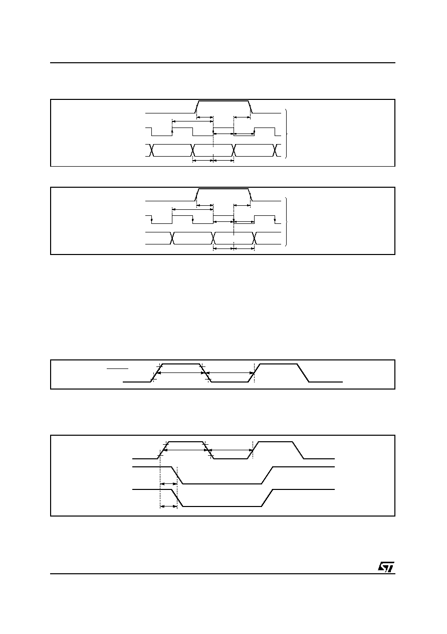
5.4.1. Audio DAC Interface
a) OCLK in output. The audio PLL is used to clock the DAC
OCLK (OUTPUT)
SDO
SCKT
LRCLK
t
sdo
t
sckt
t
lrclk
D98AU969
Pad-timing versus load
Load (pF)
Pad_timing
25
2.90ns
50
3.82ns
75
4.68ns
100
5.52ns
Cload_XXX is the load in pF on the XXX output.
pad_timing (Cload_XXX) is the propagation delay
added to the XXX pad due to the load.
tsdo = 3.5 + pad_timing (Cload_SDO) - pad_timing
(Cload_ OCLK)
tsckt = 4 + pad_timing (Cload_SCKT) - pad_timing
(Cload_ OCLK)
tlrckt = 3.5 + pad_timing (Cload_LRCCKT) -
pad_timing (Cload_ OCLK)
OCLK (INPUT)
SDO
SCKT
LRCLK
t
sdo
t
sckt
t
lrclk
D98AU970
t
hi
t
lo
t
oclk
b) OCLK in input.
Thi min = 3ns
Tlo min = 3ns
Toclk min = 25ns
tsdo = 5.5 + pad_timing (Cload_SDO) ns
tsckt = 6 + pad_timing (Cload_SCKT) ns
tlrckt = 5.5 + pad_timing (Cload_LRCKT) ns
STA013 - STA013B - STA013T
29/38
SDI
SCKR
IGNORED
VALID
IGNORED
t
_biten
t
_biten
t
sdi_hold
t
sdi_setup
D98AU971A
t
sckr_min_high
BIT_EN
SCLK_POL=0
t
sckr_min_low
t
sckr_min_period
5.4.2. Bitstream input interface (SDI, SCKR, BIT_EN) SCL_POL = 0
tsdi_setup_min = 2ns
tsdi_hold_min = 3ns
tsckr_min_hi = 10ns
tsckr_min_low = 10ns
tsckr_min_lperiod = 50ns
t_biten (min) = 2ns
SRC_INT
D98AU972
t
_src_hi
t
_src_low
5.4.3. SRC_INT
This is an asynchronous input used in "broadcast' mode.
SRC_INT is active low
t_src_low min duration is 50ns (1DSP clock period)
t_src_high min duration is 50ns (1DSP clock period)
XTI (INPUT)
XTO
CLK_OUT
t
xto
t
clk_out
D98AU973
t
hi
t
lo
5.4.4. XTI,XTO and CLK_OUT timings
txto = 1.40 + pad_timing (Cload_XTO) ns
tclk_out = 4 + pad_timing (Cload_CLK_OUT) ns
Note: In "multimedia" mode, the CLK_OUT pad is DATA_REQ. In that case, no timing is given between the XTI input and this pad.
SDI
SCKR
IGNORED
IGNORED
VALID
IGNORED
t
_biten
t
_biten
t
sdi_hold
t
sdi_setup
D99AU1038
t
sckr_min_high
BIT_EN
SCLK_POL=4
t
sckr_min_low
t
sckr_min_period
5.4.2. Bitstream input interface (SDI, SCKR, BIT_EN) SCL_POL = 1
STA013 - STA013B - STA013T
30/38
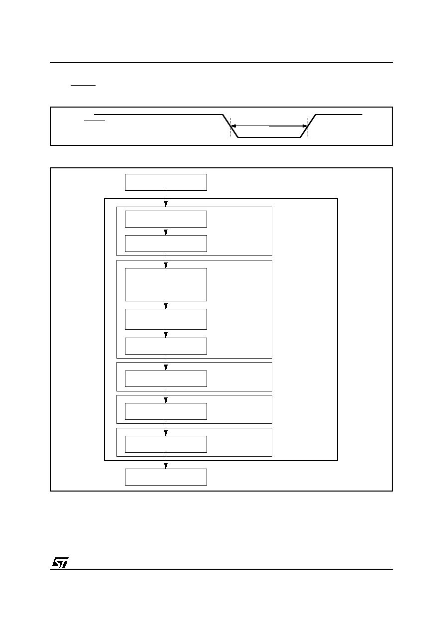
RESET
D98AU974
t
reset_low_min
5.4.5. RESET
The Reset min duration (t_reset_low_min) is 100ns
HW RESET
set
PCM OUTPUT
INTERFACE
CONFIGURATION
set
set
PCM-DIVIDER
PCM-CONF.
PLL FRAC_441_H,
PLL FRAC_441_L,
PLL FRAC_H,
PLL FRAC_L }
{
set
MFS DF_441,
MFSDF }
{
PLL
CONFIGURATION
FOR:
set
PLL CTRL
48, 44.1, 32
29, 22.05, 16
12, 11.025, 8 } KHz
∑
{
set
SCLK_POL
INPUT SERIAL
CLOCK POLARITY
CONFIGURATION
set
DATA_REQ_ENABLE
DATA REQUEST
PIN ENABLE
set
REQ_POL
DATA REQUEST
POLARITY
CONFIGURATION
RUN
set
∑
MULTIMEDIA
MODE see
{TAB 5 to TAB12}
THE OVERALL
SETTING STEPS
ARE INCLUDED IN
THE STA013
CONFIGURATION
FILE AND CAN
BE DOWNLOADED
IN ONE STEP.
STM PROVIDES
A SPECIFIC
CONFIGURATION
FILE FOR EACH
SUPPORTED
INPUT CLOCK
FREQUENCY
D98AU975
5.5. CONFIGURATION FLOW
STA013 - STA013B - STA013T
31/38
Table 5:
PLL Configuration Sequence For
10MHz Input Clock
256 Oversapling Clock
REGISTER
ADDRESS
NAME
VALUE
6
reserved
18
11
reserved
3
97
MFSDF (x)
15
80
MFSDF-441
16
101
PLLFRAC-H
169
82
PLLFRAC-441-H
49
100
PLLFRAC-L
42
81
PLLFRAC-441-L
60
5
PLLCTRL
161
Table 6:
PLL Configuration Sequence For
10MHz Input Clock
384 Oversapling Rathio
REGISTER
ADDRESS
NAME
VALUE
6
reserved
17
11
reserved
3
97
MFSDF (x)
9
80
MFSDF-441
10
101
PLLFRAC-H
110
82
PLLFRAC-441-H
160
100
PLLFRAC-L
152
81
PLLFRAC-441-L
186
5
PLLCTRL
161
Table 7:
PLL Configuration Sequence For
14.31818MHz Input Clock
256 Oversapling Rathio
REGISTER
ADDRESS
NAME
VALUE
6
reserved
12
11
reserved
3
97
MFSDF (x)
15
80
MFSDF-441
16
101
PLLFRAC-H
187
82
PLLFRAC-441-H
103
100
PLLFRAC-L
58
81
PLLFRAC-441-L
119
5
PLLCTRL
161
Table 8:
PLL Configuration Sequence For
14.31818MHz Input Clock
384 Oversapling Rathio
REGISTER
ADDRESS
NAME
VALUE
6
reserved
11
11
reserved
3
97
MFSDF (x)
6
80
MFSDF-441
7
101
PLLFRAC-H
3
82
PLLFRAC-441-H
157
100
PLLFRAC-L
211
81
PLLFRAC-441-L
157
5
PLLCTRL
161
STA013 - STA013B - STA013T
32/38
Table 9:
PLL Configuration Sequence For
14.31818MHz Input Clock
512 Oversapling Rathio
REGISTER
ADDRESS
NAME
VALUE
6
reserved
11
11
reserved
3
97
MFSDF (x)
6
80
MFSDF-441
7
101
PLLFRAC-H
3
82
PLLFRAC-441-H
157
100
PLLFRAC-L
211
81
PLLFRAC-441-L
157
5
PLLCTRL
161
Table 10:
PLL Configuration Sequence For
14.7456MHz Input Clock
256 Oversapling Rathio
REGISTER
ADDRESS
NAME
VALUE
6
reserved
12
11
reserved
3
97
MFSDF (x)
15
80
MFSDF-441
16
101
PLLFRAC-H
85
82
PLLFRAC-441-H
4
100
PLLFRAC-L
85
81
PLLFRAC-441-L
0
5
PLLCTRL
161
Table 11:
PLL Configuration Sequence For
14.7456MHz Input Clock
384 Oversapling Rathio
REGISTER
ADDRESS
NAME
VALUE
6
reserved
10
11
reserved
3
97
MFSDF (x)
8
80
MFSDF-441
9
101
PLLFRAC-H
64
82
PLLFRAC-441-H
124
100
PLLFRAC-L
0
81
PLLFRAC-441-L
0
5
PLLCTRL
161
Table 12:
PLL Configuration Sequence For
14.7456MHz Input Clock
512 Oversapling Rathio
REGISTER
ADDRESS
NAME
VALUE
6
reserved
9
11
reserved
2
97
MFSDF (x)
5
80
MFSDF-441
6
101
PLLFRAC-H
0
82
PLLFRAC-441-H
184
100
PLLFRAC-L
0
81
PLLFRAC-441-L
0
5
PLLCTRL
161
STA013 - STA013B - STA013T
33/38
5.6. STA013 CONFIGURATION FILE FORMAT
The STA013 Configuration File is an ASCII format. An example of the file format is the following:
58 1
42 4
128 15
............
It is a sequence of rows and each one can be interpreted as an I
2
C command.
The first part of the row is the I
2
C address (register) and the second one is the I
2
C data (value).
To download the STA013 configuration file into the device, a sequence of write operation to STA013 I
2
C
interface must be performed.
The following program describes the I
2
C routine to be implemented for the configuration driver:
STA013 Configuration Code (pseudo code)
download cfg - file
{
fopen (cfg_file);
fp:=1; /*set file pointer to first row */
do {
I
2
C_start_cond; /* generate I
2
C start condition for STA013 device address */
I
2
C_write_dev_addr; /* write STA013 device address */
I
2
C_write_subaddress (fp); /* write subaddress */
I
2
C_write_data (fp); /* write data */
I
2
C_stop_cond; /* generate I
2
C stop condition */
fp++; /* update pointer to new file row */
}
while (!EDF) /* repeat until End of File */
} /* End routine */
42
4
I
2
C REGISTER VALUE
I
2
C SUB-ADDRESS
D98AU976
Note:1
STA013 is a device based on an integrated DSP core. Some of the I2C registers default values are loaded after an internal DSP boot operation.
The bootstrap time is 60 micro second. Only after this time lenght, the data in the register can be considered stable.
Note 2:
Refer also to the application note 1090
STA013 - STA013B - STA013T
34/38
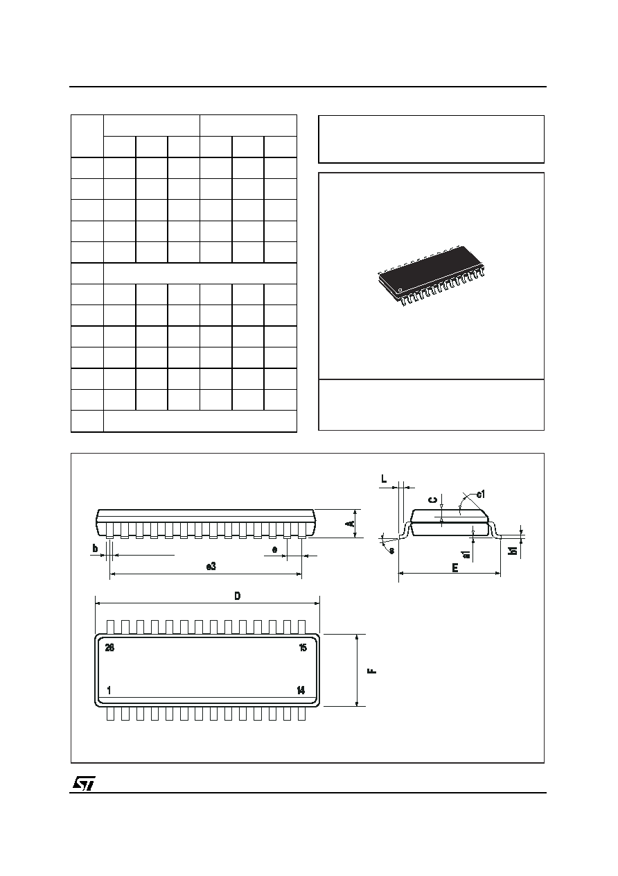
SO28
DIM.
mm
inch
MIN.
TYP.
MAX.
MIN.
TYP.
MAX.
A
2.65
0.104
a1
0.1
0.3
0.004
0.012
b
0.35
0.49
0.014
0.019
b1
0.23
0.32
0.009
0.013
C
0.5
0.020
c1
45
∞
(typ.)
D
17.7
18.1
0.697
0.713
E
10
10.65
0.394
0.419
e
1.27
0.050
e3
16.51
0.65
F
7.4
7.6
0.291
0.299
L
0.4
1.27
0.016
0.050
S
8
∞
(max.)
OUTLINE AND
MECHANICAL DATA
STA013 - STA013B - STA013T
35/38
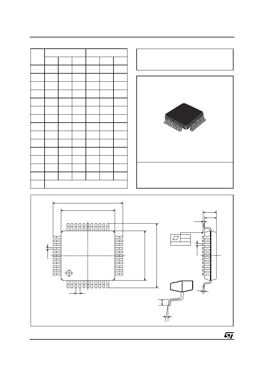
OUTLINE AND
MECHANICAL DATA
DIM.
mm
inch
MIN.
TYP.
MAX.
MIN.
TYP.
MAX.
A
1.60
0.063
A1
0.05
0.15
0.002
0.006
A2
1.35
1.40
1.45
0.053
0.055
0.057
B
0.30
0.37
0.45
0.012
0.015
0.018
C
0.09
0.20
0.004
0.008
D
11.80
12.00
12.20
0.464
0.472
0.480
D1
9.80
10.00
10.20
0.386
0.394
0.401
D3
8.00
0.315
E
11.80
12.00
12.20
0.464
0.472
0.480
E1
9.80
10.00
10.20
0.386
0.394
0.401
E3
8.00
0.315
e
0.80
0.031
L
0.45
0.60
0.75
0.018
0.024
0.030
L1
1.00
0.039
k
0∞(min.), 3.5∞(typ.), 7∞(max.)
TQFP44 (10 x 10 x 1.4mm)
A
A2
A1
B
Seating Plane
C
11
12
22
23
33
34
44
E1
E
D1
D
e
1
K
B
TQFP4410
L
0.10mm
.004
0076922 D
STA013 - STA013B - STA013T
36/38
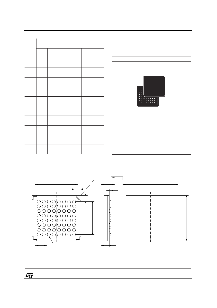
OUTLINE AND
MECHANICAL DATA
D1
D
A
0.15
A1
A2
e
f
f
A
1
2
3
4
5
6
7
8
B
C
D
E
F
G
H
E1
b (64 PLACES)
E
BALL 1 IDENTIFICATION
LFBGA64M
DIM.
mm
inch
MIN.
TYP.
MAX.
MIN.
TYP.
MAX.
A
1.700
0.067
A1
0.350
0.400
0.450
0.014
0.016
0.018
A2
1.100
0.043
b
0.500
0.20
D
8.000
0.315
D1
5.600
0.220
e
0.800
0.031
E
8.000
0.315
E1
5.600
0.220
f
1.200
0.047
LFBGA64
Body: 8 x 8 x 1.7mm
STA013 - STA013B - STA013T
37/38

Information furnished is believed to be accurate and reliable. However, STMicroelectronics assumes no responsibility for the consequences
of use of such information nor for any infringement of patents or other rights of third parties which may result from its use. No license is
granted by implication or otherwise under any patent or patent rights of STMicroelectronics. Specifications mentioned in this publication are
subject to change without notice. This publication supersedes and replaces all information previously supplied. STMicroelectronics products
are not authorized for use as critical components in life support devices or systems without express written approval of STMicroelectronics.
The ST logo is a registered trademark of STMicroelectronics.
All other names are the property of their respective owners
© 2004 STMicroelectronics - All rights reserved
STMicroelectronics GROUP OF COMPANIES
Australia ≠ Belgium - Brazil - Canada - China ≠ Czech Republic - Finland - France - Germany - Hong Kong - India - Israel - Italy - Japan -
Malaysia - Malta - Morocco - Singapore - Spain - Sweden - Switzerland - United Kingdom - United States
www.st.com
STA013 - STA013B - STA013T
38/38