 | –≠–ª–µ–∫—Ç—Ä–æ–Ω–Ω—ã–π –∫–æ–º–ø–æ–Ω–µ–Ω—Ç: STA304 | –°–∫–∞—á–∞—Ç—å:  PDF PDF  ZIP ZIP |

1/30
STA304
January 2002
This is preliminary information on a new product foreseen to be developed. Details are subject to change without notice.
s
END TO END DIGITAL AUDIO INTEGRATED
SOLUTION
s
∑ DSP Functions:
- DIGITAL VOLUME CONTROL
- SOFT MUTE
- BASS and TREBLE
- PARAMETRIC EQ PER CHANNEL
- BASS MANAGEMENT FOR SUBWOOFER
- AUTO MUTE ON ZERO INPUT DETECTION
s
4+1 DIRECT DIGITAL AMPLIFICATION
(DDXTM) OUTPUT CHANNELs
s
6 CHANNELs PROGRAMMABLE SERIAL
OUTPUT INTERFACE (by default I2S)
s
4 CHANNELs PROGRAMMABLE SERIAL
INPUT INTERFACE (by default I2S)
s
STEREO S/PDIF INPUT INTERFACE
s
Intel AC'97 LINK (rev. 2.1) INPUT INTERFACE
FOR AUDIO AND CONTROL
s
ON CHIP AUTOMATIC INPUT SAMPLING
FREQUENCY DETECTION
s
100 dB SNR SAMPLE RATE CONVERTER
(1KHz SINUSOIDAL INPUT)
s
I
2
C CONTROL BUS
s
LOW POWER 3.3V CMOS TECHNOLOGY
s
EMBEDDED PLL FOR INTERNAL CLOCK
GENERATION (1024x48 kHz = 49.152 MHz)
s
24.576 MHz EXTERNAL INPUT CLOCK OR
BUILT-IN INDUSTRY STANDARD XTAL
OSCILLATOR.
1.0 DESCRIPTION
The STA304 Digital Audio Processor is a single chip
device implementing end to end digital solution for
audio application. In conjunction with STA500 power
bridge it gives the full digital DSP-to-power high qual-
ity chain with no need for audio Digital-to-Analog con-
verters between DSP and power stage.
TQFP44
ORDERING NUMBER: STA304
PRODUCT PREVIEW
DIGITAL AUDIO PROCESSOR WITH MULTICHANNEL DDXTM
BLOCK DIAGRAM
DSP
SRC
I2S
AC`97
S/PDIF
DDX
I2S
PLL
I2C
RESET
LRCKI / SYNC
SDI_1 / SDATA_OUT
SDI_2 / SDATA_IN
RXP
RXN
BICKI / BIT_CL
SDO_1
SDO_2
SDO_3
LRCKO
BICKO
XTI
XTO
LEFT_B
LEFT_A
RIGHT_B
RIGHT_A
SLEFT_A
SLEFT_B
SRIGHT_A
SRIGHT_B
LFE_A
LFE_B
SCL
SDA
SA
RAM
ROM
CKOUT
18
1
2
3
4
19
11
10
9
7
14
15
43
43
43
43
43
43
22
21
24
23
34
33
28
27
30
29
PowerDown
44
35
EAPD
PWDN

STA304
2/30
1.0 DESCRIPTION (continued)
The device supports two main configurations as far as input sources: AC'97 input or IIS/SPDIF input: selection
is made via a dedicated pin (
AC97_MODE
pin). The AC`97 can be configured to work in two different ways:
'Full Compliant' mode and 'Proprietary' mode which enables more features. The selection of the operating mode
is done via a specific bit in a Vendor Reserved register (see bit 0: AC97_FC_mode in the CRA register, address
5Ah).
The 'Full Compliant' mode is compliant with rev. 2.1 of AC`97 link specifications.
This link can provide up to 6 input audio channels with sampling frequency of 44.1, 48, 88.2, 96 kHz, and the
related controls.
In the IIS/SPDIF mode, a stereo S/PDIF and a 4 channels three-wires programmable serial input interface work
in mutually exclusive way. Two channels with sampling frequency in the continuous range from 32 to 96 kHz
are supported by the S/PDIF interface. Up to four channels with sampling frequency varying continuously from
32kHz up to 96 kHz are supported by the programmable serial interfaces. Among the different configurations,
also the standard IIS protocol is supported.
An embedded high quality sample rate converter (SRC) resamples input data at the internal fixed sampling fre-
quency of 48 kHz for DSP operations.
The DSP is a 20x20 bit core audio processor performing several user controlled parametric algorithms, among
them are dynamic and static equalization, Bass, Treble, Volume control and more. The DSP operates at
49.152MHz (1024xfs). This frequency is generated by an internal PLL with programmable multiplication factor
(x2 or x8).
This device has 5 channels Direct Digital Amplification (DDXTM technology), performing high efficiency class-D
PWM output signals used to drive directly external power bridge stages (STA500).
In addition a 6 channel digital output programmable interface (supporting IIS standard protocol) is embedded
for applications with commercial audio D/A converters. The output sampling frequency is fixed at 48 kHz when
the interface operates as master. In addition an oversampled clock (256xfs or 512xfs) is provided externally for
the D/A converters.
An IIC interface allows full programmability of internal algorithms and control registers via an external controller.
An arbitration logic handles access conflicts to embedded control registers (which may occur as a consequence
of contemporary access to control registers by AClink, IIC and DSP blocks).
Figure 1. DSP data processing
Bass
Redir
.
Volume
Ctrl.
L, R, SL,
SR, LFE,
CNT
CNT
I2S
+
DDX
I2S
L, R, SL,
SR, LFE
Center
Volume
Ctrl.
Static
&
Dinamic
EQ

STA304
3/30
PIN CONNECTION (Top view)
PIN FUNCTION
PIN
NAME
TYPE
DESCRIPTION
PAD TYPE
1
SDI_1 / SDATA_OUT
I
Input I2S Serial Data 1 / AC97 Output Data
CMOS Schmitt In
2
SDI_2 / SDATA_IN
I/O
Input I2S Serial Data 2 / AC97 Input Data
CMOS In / CMOS Out 2mA
3
LRCKI / SYNC
I/O
Input I2S Left/Right Clock / AC97 Synch.
Clock
CMOS In / CMOS Out 2mA
4
BICKI / BIT_CLK
I/O
Input I2S Serial Clock / AC97 Bit Clock
CMOS In / CMOS Out 4mA
5
VDD_1
Digital Supply Voltage
6
GND_1
Digital Ground
7
RESET
I
Global Reset
(This pin is sensed only after 2 clock cycles)
CMOS Schmitt In Pull-Up
8
AC97_MODE
I
AC97 Enable / Disable (1=AC97; 0=I2S/
SPDIF)
CMOS Schmitt In Pull-Down
9
SDA
I/O
I2C Serial Data
CMOS In / CMOS Out 2mA
10
SCL
I
I2C Serial Clock
CMOS In
11
SA
AC97 Primary/Secondary Codec Selector
CMOS In
12
TEST_MODE
I
Test Mode (Active High)
CMOS
13
VDD_2
Digital Supply Voltage
14
XTI
I
Crystal Input (Clock input)
Analog IN
15
XTO
O
Crystal Output
CMOS Out Oscill. Pad
16
GND_2
Digital Ground
1
2
3
5
6
4
7
8
9
10
17
11
18
19
20
21
22
44
43
42
41
39
40
38
37
36
35
34
28
27
26
24
23
25
33
32
31
29
30
SDI_1/SDATA_OUT
SDI_2/SDATA_IN
LRCKI/SYNC
BICKI/BIT_CLK
VDD_1
GND_1
RESET
AC97_MODE
SDA
SCL
SA
TEST_MODE
VDD_2
XTI
XTO
GND_2
VCC
RXP
RXN
VSS
LFE_B
LFE_A
SLEFT_A
EAPD
LRCKO
SDO_1
SDO_2
SDO_3
SCKO
GND_5
VDD_5
CKOUT
PWDN
SRIGHT_B
SRIGHT_A
GND_3
VDD_3
RIGHT_B
RIGHT_A
LEFT_B
LEFT_A
GND_4
VDD_4
SLEFT_B
D00AU1160
12
13
14
15
16
STA304
4/30
PIN
NAME
TYPE
DESCRIPTION
PAD TYPE
17
VCC
Analog Supply Voltage
18
RXP
I
S/PDIF receiver positive
Analog In
19
RXN
I
S/PDIF receiver negative
Analog In
20
VSS
Analog Ground
21
LFE_B
O
Pwm LFE (subwoofer) output channel (B)
CMOS Out 3mA
22
LFE_A
O
Pwm LFE (subwoofer) output channel (A)
CMOS Out 3mA
23
SRIGHT_B
O
Pwm Surround Right output channel (B)
CMOS Out 3mA
24
SRIGHT_A
O
Pwm Surround Right output channel (A)
CMOS Out 3mA
25
GND_3
Digital Ground
26
VDD_3
Digital Supply Voltage
27
RIGHT_B
O
Pwm Right output channel (B)
CMOS Out 3mA
28
RIGHT_A
O
Pwm Right output channel (A)
CMOS Out 3mA
29
LEFT_B
O
Pwm Left output channel (B)
CMOS Out 3mA
30
LEFT_A
O
Pwm Left output channel (A)
CMOS Out 3mA
31
GND_4
Digital Ground
32
VDD_4
Digital Supply Voltage
33
SLEFT_B
O
Pwm Surround Left output channel (B)
CMOS Out 3mA
34
SLEFT_A
O
Pwm Surround Left output channel (A)
CMOS Out 3mA
35
EAPD
O
External Amplifier Powerdown (Active Low)
CMOS Out 2mA
36
LRCKO
I/O
Output I2S Left/Right Clock
CMOS In / CMOS Out 2mA
37
SDO_1
O
Output I2S Serial Data 1
CMOS Out 2mA
38
SDO_2
O
Output I2S Serial Data 2
CMOS Out 2mA
39
SDO_3
O
Output I2S Serial Data 3
CMOS Out 2mA
40
SCKO
I/O
Output I2S Serial Clock
CMOS In / CMOS Out 4mA
41
GND_5
Digital Ground
42
VDD_5
Digital Supply Voltage
43
CKOUT
O
Clock Output (12 /24 MHz)
CMOS Out 8mA
44
PWDN
I
Device Powerdown (Active Low)
CMOS In Pull-Up
PIN FUNCTION (continued)
STA304
5/30
ABSOLUTE MAXIMUM RATINGS
THERMAL DATA
ELECTRICAL CHARACTERISTCS (V
DD
from 2.9V up to 3.4V; T
amb
= 0 to 70 ∞C; unless otherwise specified)
DC OPERATING CONDITIONS
GENERAL INTERFACE ELECTRICAL CHARACTERISTICS
Note 1: The leakage currents are generally very small, < 1na. The value given here is a maximum that can occur after an electrostatic stress
on the pin.
Note 2: Human Body Model
Symbol
Parameter
Value
Unit
V
DD
Power Supply
-0.3 to 4
V
V
i
Voltage on input pins
-0.3 to VDD+0.3
V
V
o
Voltage on output pins
-0.3 to VDD+0.3
V
T
stg
Storage Temperature
-40 to +150
∞
C
T
op
Operative ambient temperature
-20 to +85
∞
C
P
DD
Power Consumption Digital
tbd
mW
P
DA
Power Consumption Analog
tbd
mW
Symbol
Parameter
Value
Unit
R
thj-amb
Thermal resistance Junction to Ambient
85
∞
C/W
Symbol
Parameter
Value
V
DD
Power Supply Voltage
3.0 to 3.6V
T
j
Operating Junction Temperature
-20 to 125
∞
C
Symbol
Parameter
Test Condition
Min.
Typ.
Max.
Unit
Note
I
il
Low Level Input Current Without
pull-up device
V
i
= 0V
-10
10
µ
A
1
I
ih
High Level Input Current
Without pull-up device
V
i
= V
DD
= 3.6V
-10
10
µ
A
1
V
esd
Electrostatic Protection
Leakage < 1
µ
A
2000
V
2
STA304
6/30
DC ELECTRICAL CHARACTERISTICS
2.0 AC'97 BANK REGISTER OVERVIEW
The AC `97 interface is compliant to `Audio Codec `97 ≠ Revision 2.1' specification, as far as the protocol used.
All the registers described in this specification, including Standard, Vendor Reserved and Extended Audio (AC
`97 2.0) registers, are available in this device, but just relevant registers which are described in paragraph 11
(Register Summary) are implemented.
The ATE mode feature has been implemented for test purpose: for related details refer to the
`Audio Codec `97
≠ Revision 2.1
' specification.
2.1 Reading AC `97 Registers
Since the AC`97 register bank has been implemented as a contiguous RAM space (from a DSP point of view)
the content of the RAM itself will be returned as the result of a read operation. This should be followed as a
general rule of thumb but, where not possible, a different approach has been used. Hereby is a list of the reg-
isters, and bits, that do not follow this rule or that have a particular handling:
∑
CodecID_0, CodecID_1
:
These two bit are respectively bits 14 and 15 of registers 28h (Extended Audio ID) and 3Ch (EWxtended
Modem ID). When a read operation of these registers is performed the returned value is based on the status
of the SA pin: CodecID_0 report the status of SA pin, CodecID_1 always report 0. Other bits of these regis-
ters return the related RAM register contents. Also note that the status of the SA pin is not readable by the
DSP.
∑
PR4
:
The bit 12 of register 26h (Powerdown, ctrl/start) is used to set the AC`97 BIT_CLK and SDATA_IN signal
to a low state. In response to a Warmers the status of this bit is set back to its default 0 value. In response
Symbol
Parameter
Test Condition
Min.
Typ.
Max.
Unit
Note
V
il
Low Level Input Voltage
0.2*V
DD
V
V
ih
High Level Input Voltage
0.8*V
DD
V
V
ol
Low Level Output Voltage
Iol = X mA
0.4*V
DD
V
1,2
V
oh
High Level Output Voltage
0.85*V
DD
V
1,2
Note 1: Takes into account 200mV voltage drop in both supply lines
Note 2: X is the source/sinc current under worst case conditions and is reflected in the name of the I/O cell according to the drive capability.
I
pu
Pull-up current
V
i
= 0V;
V
DD
= 3.3V
-25
-66
-125
µ
A
1
R
pu
Equivalent Pull-up resistance
50
K
T
R
Reset Active Time
2∑T
CK
ns
T
CK
Master Clock Period
ns
Note 1: Min condition: V
dd
= 3.0V, 125∞C Min process; Max. condition: V
dd
= 3.6 V, -20∞C max process.
DIGITAL CHARACTERISTICS-SPDIF RECEIVER (RXP,RXN pins only, SPDIF - MODE = ANALOG)
ZIN
Input Resistance
k
VTH
Dufferential Input Voltage
200
mV
VHY
Input Hysteresis
50
mV
1
49.152
------------------

STA304
7/30
to a read request the actual value of this signal is returned, not the RAM content. Due to this fact the relative
RAM register content can be incongruous.
∑
Regs
. 2Ch, 2Eh and 30h (Audio Sample Rate Control):
These three registers are used to setup the sample rate when the Variable Rate Mode is enabled. In re-
sponse to a read request on one of these registers the actual value returned can be either BB80h or AC44h,
depending on the status of an internal hardware signal; the status of this signal is updated every time a write
operation into one of these register is performed.
For more details regarding a specific bit please refer to the appropriate paragraph.
In order to be as much compliant to the specification as possible two different mode of operation has been in-
troduced. Using the
AC97_FC_Mode
configuration bit the interface can be configured in Full-Compliant mode
(default): in this mode the value returned as response to a read operation will be properly masked in order to
set `reserved' bits to 0, as from specification. This operation is performed on all registers included the Standard
or Extended Audio address space. If the Full-Compliant mode is not selected the full 16 bits data from the cor-
responding RAM register will be returned with no further manipulation.
If an odd-addressed register reading operation is performed the following scheme is adopted:
∑
Slot 0:
report valid bit set to 1 for both slot 1 and slot 2
∑
Slot 1 (address): report the odd address
∑
Slot 2 (data):
report all 0s
2.2 Writing AC `97 Registers
When a write operation into one of the available AC`97 registers is performed the entire 16 bits data word is
written into the related RAM register (also
reserved
bits are passed through). Some bits of some register may
have a corresponding
hardware register (Flip-Flop)
, used to control the internal status of the device: in this case
the value of the FF is also updated every time a write to the related RAM register is performed. The status of
these FF is reverted to their default values after a hardware reset or a software reset (writing to reg. 00h) request
has been issued; as a consequence also the DSP will have to reset the RAM register contents.
Some register may have a different behaviour from the one depicted above. Here is a brief summary of those
registers.
∑
Regs. 7Ch and 7Eh:
These are the Vendor ID1 and ID2 registers. Any write request to one of these will be ignored.
∑
Regs. 28h:
The `
Extended Audio ID Register
' is read only. Therefore any write request will be ignored.
∑
Regs. 26h:
When a write request is issued the actual data written into the RAM register is `xxxxxxxxxxxx1110', where
`x' stands for the incoming data.
∑
Regs. 2Ah:
When a write request is issued the actual data written into the RAM register is `xxxxxx0111xxxxxx', where
`x' stands for the incoming data.
∑
Regs. 32h and 34h:
Any write request into one of these
ADC sample rate register
will result in the value BB80h written into the
corresponding RAM register.

STA304
8/30
3.0 I2S INPUT INTERFACE CONFIGURATION
In order to configure the I2S input interface the
Configuration Register B
(
CRB
) can be used. Using the 3
I2SI_Align_x bits one of 6 configuration mode can be selected. Following is a table describing each one of them.
By default standard I2S input interface slave is provided (mode 1 in bits 0,1,2 of register CRB, I
2
S_BICK_Pol = 1 and
I2SI_LRCK_Pol = 0 with some register)
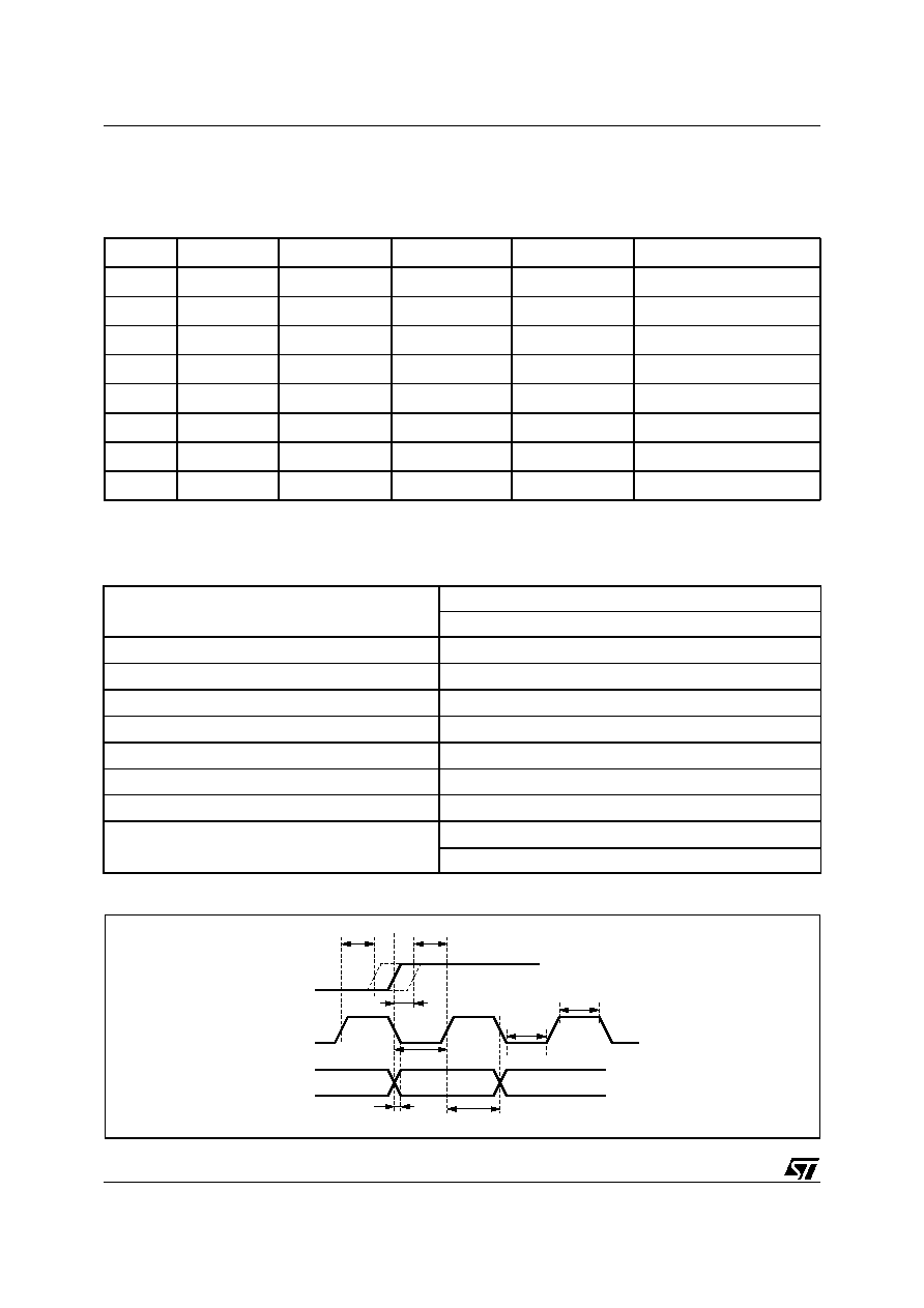
3.1 Switching characteristics (10 pf load; Fsm=32 KHz to 96KHz):
Figure 2.
MODE
# of SLOTS
W. LENGHT
ALIGNMENT
DELAY SLOT
NOTES
0
32
24
Left
No
1
32
24
Left
Yes
2
32
16
Right
No
MSb first only
3
32
24
Right
No
4
24
24
Left
No
Slave only
5
Not valid
Not valid
Not valid
Not valid
Reserved, do not use.
6
24
16
Right
No
MSb first only. Slave only
7
24
24
Right
No
Slave only
BICKI frequency (master mode):
(slave mode):
3.072MHz
Max 6.4 MHz
BICKI pulse width low (T
0
) (slave mode):
min 40 ns.
BICKI pulse width high (T
1
) (slave mode):
min 40 ns.
BICKI active to LRCKI edge delay (T
2
):
min 20 ns.
BICKI active to LRCKI edge setup (T
3
):
min 20 ns.
SDI valid to BICKI active setup (T
4
):
min 20 ns.
BICKI active to SDI hold time (T
5
):
min 20 ns.
BICKI falling to LRCKI edge (T
6
) (master mode):
min 3 ns; max 9 ns.
T
2
T
3
T
0
T
1
T
5
T
4
T
6
D00AU1244
LRCKI
BICKI
SDI
STA304
9/30
4.0 I2S OUTPUT INTERFACE CONFIGURATION
In order to configure the I2S output interface the
Configuration Register B
(
CRB
) can be used. Using the 3
I2SO_Align_x bits one of 6 configuration mode can be selected. Following is a table describing each one of
them.
By default standard I2S output interface master is provided (mode 1 in bits 8,9,10 of register CRB,
I2SO_BICK_Pol = 1 and I2SO_LRCK_Pol = 0 in the same register)
4.1 Switching characteristics (10 pf load; Fsm=48 KHz):
Figure 3.
MODE
# of SLOTS
W. LENGHT
ALIGNMENT
DELAY SLOT
NOTES
0
32
24
Left
No
1
32
24
Left
Yes
2
32
16
Right
No
MSb first only
3
32
24
Right
No
4
24
24
Left
No
Slave only
5
Not valid
Not valid
Not valid
Not valid
Reserved, do not use.
6
24
16
Right
No
MSb first only. Slave only
7
24
24
Right
No
Slave only
SCKO frequency (master mode):
64 Fsm
(slave mode):
64 Fsm
SCKO pulse width low (T
0
) (slave mode):
min 40 ns.
SCKO pulse width high (T
1
) (slave mode):
min 40 ns.
SCKO active to LRCKO edge delay (T
2
):
min 20 ns.
SCKO active to LRCKO edge setup (T
3
):
min 20 ns.
SDO valid to SCKO active setup (T
4
):
min 20 ns.
SCKO active to SDO hold time (T
5
):
min 20 ns.
SCKO falling to LRCKO edge (T
6
) (master mode):
min 2 ns; max 8 ns.
SCKO falling to SDO edge(T
7
) (master mode):
min 2 ns; max 8 ns.
(slave mode):
min 6 ns; max 17 ns
T
2
T
3
T
0
T
1
T
5
T
7
T
4
T
6
D00AU1245
LRCKO
BICKO
SDO

STA304
10/30
5.0 DDX OUTPUT SWITCHING
The 5 DDX output (L,R,SL,SR,LFE) are ternary modulated PWM, designed to drive directly STA50X power
bridge ICs or any custom discrete power. The PWM output frame is delayed from channel to channel in order
to reduce the crosstalk at the stereo STA50X device at low audio dynamics. The PWM order in the STA304 is:
≠ L
≠ LS
≠ R
≠ RS
with 32 ticks (of master clock) or ~640ns between the beginning of each PWM frame (frame period is ~2.6usec).
The LFE PWM signal is independently generated (synchronous with LS PWM output), because it is intended to
be used alone on a mono-configured STA50x IC (no crosstalk issues).
In this way the low-modulated level PWM signal of different channels switches when the others are at zero level,
so when the output power is in dump state (both terminals of the speaker loads are connected to ground), caus-
ing no noise cross-injection.
Best performances are obtained when only front channels (L/R) or rear channels (SL/SR) are fed to a single
STA50X device, because the PWM frames of L an R have the maximum distance of ~1.3usec (same for SL and
SR).
Of course crosstalk is anyway removed with a good power supply design/layout for STA50x ICs (low impedance
stage and low inductance loop between powerVDD and GND). See application notes for more details

STA304
11/30
6.0 SAMPLE RATE CONVERTER
The sample rate converter resamples the selected input data source in order to send to the DSP an audio
stream with a fixed frequency of 48 KHz. The following picture show the basic architecture.
Figure 4.
The selection between X2 Fir interpolation or direct antialiasing Filter on input data is made automatically by the
threshold selector block. If the input sampling frequency (measured by DRLL) is high than the SRC threshold
(see Table 2 section 12.9), the direct antialising filter is selected, otherwise if the input frequency is lower than
the SRC threshold, the X2 FIR filter is added the data path. A 1kHz hysteresis is fixed around the SRC threshold
nominal values of tab. 2 section 12.9, to prevent unstable oscillations. In figure 5 the DRLL lock phase is shown
for 32kHz,44.1kHz, 48kHz and 96kHz input frequency. Note that only after this phase (including the flat part of
the graph) the SRC performances are in spec.
Figure 5. DRLL lock delay
Interpolation
FIR x2
Anti-Alias
FILT
Interpolation
FIR x2
2 x Fs
Fs
Fs
DATA_IN
Sinc 6
Async.
DRLL
LRCK_IN
Thresh.
Selector
RATIO
4xFs or 2xFs
DATA_OUT
48KHz
0
0.05
0.1
0.15
0.2
0.25
0
1
2
3
4
5
6
7
8
9
10
x 10
4
Second
Esimated F
requency
STA304
12/30
7.0 DAP INPUT STAGE
The device provides 3 mutually exclusive input interfaces: I2S, S/PDIF and AC`97. Hereby is a small description
of the characteristics for each of them and a table showing how to select it.
Figure 6.
7.1 Input from I
2
S
Using this input interface a maximum of 4 channels can be sent to the DSP. As detailed in the related paragraph
this I/F can be configured both as master or slave. When in master the sampling frequency is fixed to 48 KHz
and the SRC can be bypassed using the
SRC_Bypass
configuration bit (in CRA register). If slave operation is
selected the full range between 32KHz and 96KHz is supported but the SRC must always be in the processing
path (no bypass). In order to select this interface the AC97_MODE pin must be tied to GND and the
I2S_SPDIF_Sel bit must be 0. This input configuration requires that SA pin (#11) is connected to ground
7.2 Input from S/PDIF
This interface is compliant with the AES/EBU IEC 958, S/PDIF and EIAJ CP-340/1201 professional and con-
sumer standards. The full range from 32 KHz up to 96 KHz is supported but the SRC bypass option must be
switched off. Using the
SPDIF_Mode
bit this interface can be configured as digital or analog input. If the analog
mode is selected the line receiver can decode differential as well as single ended inputs. The receiver consists
of a differential input
Schmitt Trigger
comparator with 50 mV of hysteresis, which prevents noisy signals from
corrupting the data recovered. The minimum input differential voltage is 200 mV.
If the digital mode is selected only the single ended operation is supported; the input signal should be CMOS
compliant.
In order to select this interface the AC97_MODE pin must be tied to GND and the I2S_SPDIF_Sel must be 1.
This input configuration requires that SA pin (#11) is connected to ground
7.3 Input from AC`97
In order to select this interface the AC97_MODE pin must be tied to VDD (I2S_SPDIF_Sel bit `is don't care).
The AC`97 interface can be configured either as primary or secondary device using the external configuration
pin SA.
YRAM
SRC
AC97
I2S
S/PDIF
LEFT
RIGHT
SL/CENTER
SR
CENTER
LFE
AC97_Sel
I2S_SPDIF_Sel
SRC_Bypass
PLL
MCK
PLL_Factor
PLL_Bypass
XTI
DSP
DDX
I2S
I2C
YRAM
LEFT
RIGHT
SL/CENTER
SR
CENTER
LFE
/1024
/2 or /8
LRCK
CK_OUT
LRCK
STA304
13/30
This interface support 4 sampling frequencies, according to the
Variable and Double Rate Audio Codec `97
specification. The following table summarize the slot usage for each one the these frequencies:
* Slots 3, 4 and 6 are always requested. Slots 10, 11 and 12 are requested only when needed.
The following table summarize the different input possibilities:
* In this configuration the BYPASS is always active, regardless SRC_Bypass bit in reg. 5Ah
8.0 PLL
In order to generate the internal 49.152 MHz clock a low-jitter PLL has been included in the device. It can be config-
ured to work either with a multiplication factor of x8 or x2, in order to fit an external frequency reference of 6.144 MHz
or, respectively, 24.576 MHz. This could be useful when the device is configured to work in AC`97 slave mode where
the master clock is 24.576 MHz. To select the multiplication factor the
PLL_Factor
bit can be used.
Using the
PLL_Bypass
bit the PLL section can be bypassed, allowing direct connection of the internal clock to
the XTI pin. When this option is selected an external frequency of 49.152 MHz should be provided to the device.
In this condition the PLL is automatically powered-down.
9.0 POWERDOWN MANAGEMENT
The powerdown capability and its logic behaviour is shown in
Figure 7 - Powerdown management
. Basically
there are three powerdown requests which comes from the extern of the device and will cause a different pow-
erdown condition:
-
External PWDN pin ≠ this signal will turn-off the device which, as a consequence, will enter the power-
down mode (all the device clocks are stopped). The device will exit this state as soon as the PWDN pin
is deasserted.
-
PR5 bit (reg. 26h, bit 13) ≠ Setting this bit will cause a partial powerdown of the device: infact all the clocks
will be suspended, except that used to keep the AC97 and I2C cells alive. In this way, using either of these
input interfaces, it'll be possible to resume from this state simply resetting the PR5 bit.
-
EAPD bit (reg.26h, bit 15) ≠ The External Amplifier PowerDown bit controls the state of the related pin
(EAPD) which, in turn, is used to switch off the external power chip.
Freq.
Slot 3
Slot 4
Slot 6
Slot 7
Slot 8
Slot 9
Slot 10
Slot 11
Slot 12
48
Left
Right
Center
Surr.L
Surr.R
LFE
44.1
Left
Right
Surr.L
Surr.R
88.2 *
Left
Right
Center
Left (n+1)
Right (n+1)
Center (n+1)
96
Left
Right
Center
Left (n+1)
Right (n+1)
Center (n+1)
Input from
Channels
Available Freq. (KHz)
Bypass
Notes
I2S (Master)
4
48
Yes
Bypass is user selectable
I2S (Slave)
4
32..96
No
S/PDIF
2
32..96
No
AC`97
6
48
Yes *
Left, Right, SL, SR, Center, LFE
AC`97
3
96
No
Left, Right, Center
AC`97
4
44.1 (VRA)
No
Left, Right, SL, SR
AC`97
3
88.2 (VRA)
No
Left, Right, Center
STA304
14/30
Figure 7. Powerdown management
In order to avoid any possible pop-noise while switching between the various powerdown modes a particular
masking technique has been adopted to drive the actual controlling signals: as shown in the above figure the 3
powerdown requests will inform the DSP using the related bits in specific registers. After that the DSP performs
a software fade-out of the channels volume and, finally, activates the MUTE flags of the various channels.
The actual controlling lines are the result of a logical AND operation between the relative request signals and
the 4 channel MUTE bits (LR, LFE, SL and SR).
Moreover the external power chip will be turned off (via the EAPD pin) not only as a consequence of an EAPD request,
but also as a consequence of a PR5 or PWDN requests: this solution will prevent any possible noise or glitch.
&
Internal CK disable
&
Chip powerdown
&
DSP
Requests
OR
EAPD (reg. 26h, bit 15)
PWDN pin (reg.7EFh, bit0)
PR5 (reg.26h, bit 13)
EAPD pin (ACTIVE Low)
(Active Low)
LR
LFE
SL
SR
&
LR
reg. 02h bit 15
LFE
reg. 36h bit 15
SR
reg. 38h bit 07
SL
reg. 38h bit 15
STA304
15/30
10.0 BASS MANAGEMENTAND EQ
The STA304 has the ability to redirect the sound to the SBW channel and to pass each channel through a 4-
stage cascaded 2nd order IIR filter. With the combination of the DDX gain/compressor (CRA register bits 2-3)
a dynamic EQ can be implemented. Beside that, a special Side-Firing sound can be achieved by enabling this
feature available with the ready made filter topology on the surround channels.
10.1 Bass Redirection
Figure 8.
There is an option to redirect each input channel to the SBW output channel. The Scale factor of each channel
should be set with values in the range of 0 (no redirection) to -1 (full redirection). About setting the scaling factors
registers, see paragraph 10.
The redirection is taking place when the bit 0 of the Bass Management Register (add.72h) is set (see section
12.13).
Together with the static EQ option (following section), by setting appropriate filters, a full bass management so-
lution is available.
(*) Note: C and LFE channels are available only with 6 channels AC97 input. In case of 4 channels I
2
S, only L, R, LS, RS are
available
10.2 Static EQ
Figure 9.
Phantom
LR Filter
LR Filter
Sur Filter
Sur Filter
+
Scale
L
Scale
C
Scale
R
Scale
LS
Scale
RS
Scale
LFE
SBW
Filter
L
C
R
LS
RS
LFE
L
R
LS
RS
SBW
(
IIS
C)
(*)
(*)
Scale in
Factor
bi-quad0
bi-quad1
bi-quad2
bi-quad3
Input
Output

STA304
16/30
Each channel has a 4 stage cascaded 2nd order filter. The user can set each filter coefficients (see paragraph
10). The coefficient for the Left and Right channels are common, as well as the coefficients for the surrounds.
There is also an input scaling factor for each channel which can be set with values from 0 to -1. The scaling
factor should be set to an appropriate value that will prevent the filter going into saturation.
The Static EQ filters are activated by setting Static EQ and Side Firing register (add. 70h, see section 12.12).
10.3 Surround Side Firing
Instead of the normal filters described in the previous section above, a special topology is available for the sur-
round channels:
Figure 10.
By designing appropriate filters special surround sound can be achieved for a system which its surround speak-
ers are located next to the front speakers and are rotated to the sides (see picture). The Side firing topology is
enabled by setting Static EQ and Side Firing register (add. 70h, see section 12.12).
Figure 11. Speaker System with Side-Firing positioning
Scale in
Factor
bi-quad0
bi-quad1
+
and Phase
Invering
+
Left Surround
Input
Left Surround
Output
bi-quad2
bi-quad3
Scale in
Factor
bi-quad0
bi-quad1
Right Surround
Input
bi-quad2
bi-quad3
Right Surround
Output

STA304
17/30
11.0 COEFFICIENT HANDLING
In order to implement the Static EQ filters and the Bass management, a RAM space for user coefficients has
been included in this device: starting from address 240h (YRAM) there are 69 x 20 bit registers available for this
purpose. In order to be able to read or write into these registers an indirected addressing approach must be
followed by the application software. As showed in Figure 8 there are two AC'97 dedicated registers (4 x 8 bits
registers from I2C point of view) to access the coefficient table. In register 78h (78h + 79h in I2C addressing)
the 16 low bits of the coefficient are stored (by the user in case of a write operation, by the logic in case of a
read operation); the higher 4 bits are stored in the lowest nibble of register 7Ah (7Bh in I2C addressing). The
address of the coefficient on which the R/W operation must be performed is stored in the high byte of register
7Ah. The address is made adding the coefficient index to the base location 40h.
To select between Read or Write operation the 'R' bit in register 7Ah (7Bh in I2C addressing) must be properly
setup. The actual read/write operation will start after the register 7Ah (7Bh in I2C addressing) has be written.
The following paragraphs will explain this in more details.
Figure 12. Coefficient registers usage
11.1 Reading a coefficient value
Depending on the bus used to read the coefficient the following steps must be followed:
∑
Reading from AC'97
≠ write 8 bit INDEX 40h and R/W bit at AC`97 address 7Ah
≠ read 16 lower data bits at AC`97 address 78h
≠ read 4 higher data bits at AC`97 address 7Ah
∑
Reading from I
2
C
≠ write 8 bit address at I2C address 7Ah coeff INDEX + 40h
≠ write R/W bit at I
2
C address 7Bh
≠ read 8 middle data bits at I
2
C address 78h
≠ read 8 lower data bits at I
2
C address 79h
≠ read 4 higher data bits at I
2
C address 7Bh
11.2 Writing a coefficient value
Depending on the bus used to write the coefficient the following steps must be followed:
∑
Writing from AC'97
≠ write 16 lower bit data at AC`97 address 78h
≠ write 8 bit INDEX + 40h and R/W bit and 4 higher data bits at AC`97 address 7Ah
∑
Writing from I2C
≠ write 8 middle data bits at I2C address 78h
≠ write 8 lower data bits at I2C address 79h
≠ write 8 bit address at I2C address 7Ah coeff INDEX + 40h
≠ write 4 higher data bits and R/W bit at I2C address 7Bh
Coefficient[15..0]
Coeff. Address (8 bits)
Coefficient[19..16]
R-x-x-x
Bit 0
Bit 15
78h
7Ah
AC`97
78h
7Ah
I2C
79h
7Bh
R : set this bit to 1 for reading a coefficient, 0 for writing it.
STA304
18/30
11.3 Coefficient map
Filter coefficients:
CHx0 = b2
CHx1 = (b0)-1
CHx2 = a2
CHx3 = (a1)/2
CHx4 = (b1)/2
Index
(decimal)
index (hex)
coefficient
default value
0
0h
20 LR filter coef.
LR00 (b2)
00000h
1
1h
LR01 (b0-1)
00000h
...
...
...
...
4
4h
LR04 (b1/2)
00000h
5
5h
LR10 (b2)
00000h
...
...
...
...
19
13h
LR34 (b1/2)
00000h
20
14h
20 Surrounds
filter coef.
SUR00
00000h
...
...
...
...
39
27h
SUR34
00000h
40
28h
20 SBW filter
coef.
SBW00 (b2)
00032h
41
29h
SBW01 (b0-1)
80032h
42
2Ah
SBW02 (a2)
7C7EAh
43
2bh
SBW03 (a1/2)
81C6Fh
44
2Ch
SBW04 (b1/2)
00032h
45
2dh
SBW10
00000h
...
...
...
...
59
3bh
SBW34
00000h
60
3Ch
3 scale in factors
-scale_in LR
80000h
61
3dh
-scale_in SUR
80000h
62
3Eh
-scale_in SBW
80000h
63
3Fh
6 SBW
redirection
factors
-scale_L
SBW
C0000h
64
40h
-scale_R
SBW
C0000h
65
41h
-scale_LS
SBW
C0000h
66
42h
-scale_RS
SBW
C0000h
67
43h
-scale_C
SBW
C0000h
68
44h
-scale_LFE
SBW
80000h

STA304
19/30
where CH stands for LR,SUR or SBW and x stands for the filter number (0..3).
The filter equation is Yn = Xn+((b0)-1)*Xn + 2*((b1)/2)*Xn-1 + b2*Xn-2 - 2*((a1)/2)*Yn-1 - a2*Yn-2 =
= b0*Xn + b1*Xn-1 + b2*Xn-2 - a1*Yn-1 - a2*Yn-2
The coefficient registers are 20 bits wide and should be in the range [-1..1) (80000h to 7ffffh).
Scaling factor registers:
For the filters Xn = - (-scale_in) * CHn , where CHn is the value before scaling and Xn is the input to the filter.
For the SBW redirection SBWn = -S (-scale_CH)*CHn
The scaling factor registers are 20 bits wide and should be in the range [-1..0] (80000h to 00000h).
SBW redirection: -1 for maximum redirection and 0 for no redirection.
Filter scaling: -1 for maximum input and 0 for no input to filter.
12.0 I
2
C BUS SPECIFICATION
The STA304 supports the I
2
C protocol. This protocol defines any device that sends data on to the bus as a trans-
mitter and any device that reads the data as a receiver. The device that controls the data transfer is known as
the master and the others as the slave. The master always starts the transfer and provides the serial clock for
synchronisation. The STA304 is always a slave device in all its communications.
16bit registers are addressed as two 8 bit registers. The high byte has even address, while the low byte has odd
address. For example, reading from register 02 (16bit) means read registers 02 (HIGH BYTE) and 03 (LOW
BYTE) from I
2
C.
12.1 COMMUNICATION PROTOCOL
12.1.1Data transition or change
Data changes on the SDA line must only occur when the SCL clock is low. SDA transition while the clock is high
are used to identify START or STOP condition.
12.1.2Start condition
START is identified by a high to low transition of the data bus SDA signal while the clock signal SCL is stable
in the high state.A START condition must precede any command for data transfer.
12.1.3Stop condition
STOP is identified by low to high transition of the data bus SDA signal while the clock signal SCL is stable in the
high state. A STOP condition terminates communications between STA304 and the bus master.
12.1.4Acknowledge bit
An acknowledge bit is used to indicate a successful data transfer. The bus transmitter, either master or slave,
releases the SDA bus after sending 8 bit of data.
During the 9th clock pulse the receiver pulls the SDA bus low to acknowledge the receipt of 8 bits of data.
12.1.5Data input
During the data input the STA304 samples the SDA signal on the rising edge of the clock SCL.
For correct device operation the SDA signal has to be stable during the rising edge of the clock and the data
can change only when the SCL line is low.
12.2 DEVICE ADDRESSING
To start communication between the master and the STA304, the master must initiate with a start condition.
Following this, the master sends onto the SDA line 8 bits (MSB first) corresponding to the device select address

STA304
20/30
and read or write mode.
The 7 most significant bits are the device address identifier, corresponding to the I
2
C bus definition.
The STA304 I
2
C interface address is 0011110 .
The 8th bit (LSB) is the read or write operation RW, this bit is set to 1 in read mode and 0 for write mode. After
a START condition the STA304 identifies on the bus the device address and, if a match is found, it acknowledg-
es the identification on SDA bus during the 9th bit time. The following byte after the device identification byte is
the internal space address.
12.3 WRITE OPERATION
Following a START condition the master sends a device select code with the RW bit set to 0. The STA304 ac-
knowledges this and waits for the byte of internal address. After receiving the internal bytes address the STA304
again responds with an acknowledge.
12.3.1Byte write
In the byte write mode the master sends one data byte, this is acknowledged by STA304. The master then ter-
minates the transfer by generating a STOP condition.
12.3.2Multibyte write
The multibyte write mode can start from any internal address. The transfer is terminated by the master gener-
ating a STOP condition.
Figure 13. Write Mode Sequence
Figure 14. Read Mode Sequence
DEV-ADDR
ACK
START
D98AU825B
RW
SUB-ADDR
ACK
DATA IN
ACK
STOP
BYTE
WRITE
DEV-ADDR
ACK
START
RW
SUB-ADDR
ACK
DATA IN
ACK
STOP
MULTIBYTE
WRITE
DATA IN
ACK
DEV-ADDR
ACK
START
D98AU826A
RW
DATA
NO ACK
STOP
CURRENT
ADDRESS
READ
DEV-ADDR
ACK
START
RW
SUB-ADDR
ACK
DEV-ADDR
ACK
STOP
RANDOM
ADDRESS
READ
DATA
NO ACK
START
RW
DEV-ADDR
ACK
START
DATA
ACK
DATA
ACK
STOP
SEQUENTIAL
CURRENT
READ
DATA
NO ACK
DEV-ADDR
ACK
START
RW
SUB-ADDR
ACK
DEV-ADDR
ACK
SEQUENTIAL
RANDOM
READ
DATA
ACK
START
RW
DATA
ACK
NO ACK
STOP
DATA
RW=
HIGH
STA304
21/30
13.0 REGISTER SUMMARY
13.1 Reset Register (add. 00h)
Writing any value to this register performs a register reset, which causes all registers to revert to their default
values. Reading this register returns 00E4h as it is the ID code of the part and its 3D Stereo Enhancement type
(See AC'97 revision 2.1 specification, section 6.3.1).
13.2 LR Volume Register (add. 02h)
This register manage the stereo (both right and left channels) output signal volumes. The MSB of the register
is the mute bit. When this bit is set to 1 the level for that channel is set at -
dB. ML6 through ML0 is for the left
channel level, MR6 through MR0 is for the right channel.
There are two options: in 'Full Compliance' operating mode (bit 0 in the CRA register, address 5Ah, is set to '0')
only 6 bits are active (Mx0 to Mx5) and each step corresponds to 1.5 dB. In 'Proprietary' mode (bit 0 in the CRA
register is set to '1') Mx0 to Mx6 can have the values between 0h to 68h (110 1000) and each step corresponds
to 1dB. Greater values are undefined.
The default value is 8000h (1000 0000 0000 0000), which corresponds to 0 dB attenuation with mute on.
'Full Compliance' Mode
'Proprietary' Mode
D15
D14
D13
D12
D11
D10
D9
D8
D7
D6
D5
D4
D3
D2
D1
D0
0
0
0
0
0
0
0
0
1
1
1
0
0
1
0
0
D15
D14
D13
D12
D11
D10
D9
D8
D7
D6
D5
D4
D3
D2
D1
D0
Mute
ML6
ML5
ML4
ML3
ML2
ML1
ML0
X
MR6
MR5
MR4
MR3
MR2
MR1
MR0
Mute
Mx6...Mx0
Function
0
x00 0000
0 dB Attenuation
0
x01 1111
46.5dB Attenuation
0
x11 1111
94.5dB Attenuation
1
xxx xxxx
dB Attenuation
Mute
Mx6...Mx0
Function
0
000 0000
0 dB Attenuation
0
001 1111
31dB Attenuation
0
011 1111
63dB Attenuation
...
...
0
110 0001
97
dB Attenuation
0
110 0010
99dB Attenuation
0
110 0011
100dB Attenuation
0
110 0100
102dB Attenuation
0
110 0101
104dB Attenuation
0
110 0110
107dB Attenuation
0
110 0111
111dB Attenuation
0
110 1000
dB Attenuation
1
xxx xxxx
dB Attenuation
STA304
22/30
13.3 Tone Control Register (add. 08h)
This register support tone controls (bass and treble). The step size is 2dB. Writing a 0000h corresponds to
+12dB of gain. Center frequencies (from which gains are measured) are 160Hz for Bass and 5,000Hz for Treble.
The default value is 0F0Fh, which corresponds to bypass of bass or treble gain. The tone feature is implemented
only on the L and R front channel.
13.4 Powerdown Ctrl/Staus Register (PCSR) : add. 26h
NOTE: Bits D0..D3 will be masked to the showed value before writing into the RAM registers, other bits will simply pass through.
D15
D14
D13
D12
D11
D10
D9
D8
D7
D6
D5
D4
D3
D2
D1
D0
X
X
X
X
BA3
BA2
BA1
BA0
X
X
X
X
TR3
TR2
TR1
TR0
TR3... TR0 or BA3... BA0
Function
0000
+12 dB of gain
0001
+10 dB of gain
0010
+8 dB of gain
0011
+6 dB of gain
0100
+4 dB of gain
0101
+2 dB of gain
0110
+1 dB of gain
0111
0 dB of gain
1000
-1 dB of gain
1001
-2 dB of gain
1010
-4 dB of gain
1011
-6 dB of gain
1100
-8 dB of gain
1101
-10 dB of gain
1110
-12 dB of gain
1111
Bypass
D15
D14
D13
D12
D11
D10
D9
D8
D7
D6
D5
D4
D3
D2
D1
D0
EAPD
PR5
PR4
1
1
1
0
BIT
R/W
RST
NAME
DESCRIPTION
12
R/W
0
PR4
Setting this bit to 1 the BIT_CLK and the SDATA_IN signal will be fixed to the
digital low level. To resume the normal operation either an hardware reset or a
softReset
must be performed.
13
R/W
0
PR5
In order to set the device in a powerdown-like condition this bit must be set to 1.
This will stop the device internal clock: only the PLL and AC`97, I
2
C clocks will
still be running. DSP should start power-down sequence in order to accomplish
this request.
15
R/W
1
EAPD
The value of this bit should be checked by the DSP in order to recognize an
external power amplifier power-down request. As a consequence the DSP
should start the power-down sequence (volume fade-out)
STA304
23/30
13.5 Extended Audio ID Register (add. 28h)
The Extended Audio ID is a read only register that identifies which extended audio features are supported (See
AC'97 revision 2.1 specification, section A.2.1). The extended features supported are Variable Rate PCM Audio
(VRA), Double- Rate PCM Audio (DRA), PCM Center (CDAC), PCM Surround (SDAC) and PCM LFE (LDAC).
Codec_ID0 report the status of SA pin. Codec_ID1 always report 0. Hence, the configurations are primary (00)
if SA pin is 0 or Secondary (01) if SA pin is 1.
13.6 Extended Audio Status and Control Register (add. 2Ah)
∑ VRA= 1 enables Variable Rate Audio mode (sample rate control registers and SLOTREQ signaling)
∑ DRA= 1 enables Double- Rate Audio mode
Bits D9- D6 are read only status of the extended audio feature readiness. When a write request is issued the
actual data written into the RAM register is 'xxxxxx0111xxxxxx'.
For more details refer to AC'97 rev 2.1, section A.2.2
13.7 Audio Sample Rate Control Registers (add. 2Ch - 34h)
In VRA mode, two frequencies are supported 48000(BB80h) Hz and 44100(AC44h) Hz. If one of these value
written to the 2Ch register, that value will be echoed back when read, otherwise the closest (higher in case of a
tie) sample rate supported is returned. The content of 2Eh and 30h registers is copied from the 2Ch register.
If the Double Rate Audio (DRA) mode is active, the sample rate programmed will be multiplied by 2x. For ex-
ample: When running at 88.2 kHz, the DRA bit will be programmed to 1, and the sample rate programmed would
be 44.100.
The default value after cold or warm register reset for these registers (BB80h) is 48 kHz.
The content of the ADC sample rate registers (32h and 34h) stays always BB80h.
13.8 6-Channel Volume Control Register (add. 36h - 38h)
These read/write registers control the output volume of the optional four PCM channels, and values written to
the fields behave the same as the Play Master Volume Register (Index 02h), which offers attenuation but no
gain. There is an independent mute (1= on) for each channel.
The default value after reset for this registers (8080h) corresponds to 0 dB attenuation with mute on.
D15
D14
D13
D12
D11
D10
D9
D8
D7
D6
D5
D4
D3
D2
D1
D0
0
ID0
0
0
0
0
0
1
1
1
0
0
0
0
1
1
D15
D14
D13
D12
D11
D10
D9
D8
D7
D6
D5
D4
D3
D2
D1
D0
0
1
1
1
DRA
VRA
D15
D14
D13
D12
D11
D10
D9
D8
D7
D6
D5
D4
D3
D2
D1
D0
SR15
SR14
SR13
SR12
SR11
SR10
SR9
SR8
SR7
SR6
SR5
SR4
SR3
SR2
SR1
SR0
D15
D14
D13
D12
D11
D10
D9
D8
D7
D6
D5
D4
D3
D2
D1
D0
Mute
LFE6 LFE5 LFE4 LFE3
LFE2
LFE1 LFE0
Mute
CNT6 CNT5 CNT4 CNT3 CNT2 CNT1
CNT0
Mute
LSR6
LSR5
LSR4
LSR3
LSR2
LSR1
LSR0
Mute
RSR6
RSR5 RSR4
RSR3
RSR2
RSR1
RSR0
STA304
24/30
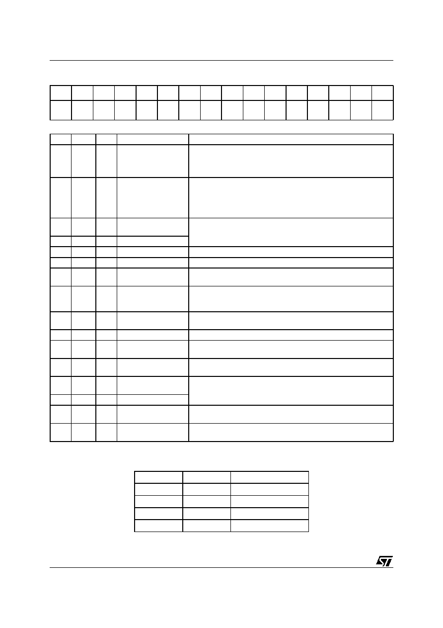
13.9 Configuration Register A (CRA) : add. 5Ah
NOTE: In TEST_MODE -> PLL_Bypass = 0.
Table 1. SRC Threshold
D15
D14
D13
D12
D11
D10
D9
D8
D7
D6
D5
D4
D3
D2
D1
D0
SRC_By
pass
DRLL_d
bg
SRC_TH
R_1
SRC_TH
R_0
SPDIF_
Mode
I2S_SP
DIF_Sel
MCKOU
T_Mode
PLL_By
pass
PLL_Fac
tor
DDX_P
wrMode
DDX_ZD
_Enable
DDX_Rst DDX_Ga
in_1
DDX_Ga
in_0
I2SI_DBU
FF_Mode
AC97_F
C_Mode
BIT
R/W
RST
NAME
DESCRIPTION
0
R/W
0
AC97_FC_Mode
AC'97 Full Compliant Mode (0 to enable). When in FC mode any read
of registers will return only valid bits: bits marked as `reserved' by
AC'97 v2.0 specification will return 0, regardless of the RAM
contents.
1
R/W
0
I2SI_DBUFF_Mode
Enable DoubleBuffer mode for the I2S input interface (write1 to
enable this option) . This is strongly required if this interface is
operated in slave mode at 48KHz, synchronous with the input source.
In this condition also Sample Rate Converter Bypass is suggested to
omprove performances.
2
R/W
0
DDX_Gain_0
DDX Gain setting (LSb/MSb). These two bits, concatenated, will set
the DDX stage gain and the compression as shown in Table 1.
3
R/W
0
DDX_Gain_1
4
R/W
1
DDX_Rst
DDX Reset (active high)
5
R/W
1
DDX_ZD_Enable
DDX Zero Detect feature. If this bit is 1 the feature is enabled.
6
R/W
1
DDX_PwrMode
DDX Power Mode (TRUTH Table). Using this bit it is possible to select
the truth table used by the DDX digital output stage (1 = ST standard)
7
R/W
0
PLL_Factor
PLL Factor (x2 or x8). It should be used according to the input
frequency provided to the device: 1 (x8) when 6.144 MHz are
provided, 0 (x2) when 24.576 MHz.
8
R/W
1
PLL_Bypass
PLL Bypass. Setting this bit to 0 will bypass the PLL; internal master
clock will be directly connected to XTI pin.
9
R/W
0
MCKOUT_Mode
MckOut mode: 12.288 MHz (1) or 24.576 MHz (0).
10
R/W
0
I2S_SPDIF_Sel
I2S - S/PDIF Selector. Select the input source: set to 0 for I2S input, 1
for S/PDIF input.
11
R/W
0
SPDIF_Mode
S/PDIF Mode. Set to 0 to select Analog mode, 1 to select Digital
mode.
12
R/W
1
SRC_THR_0
Sample Rate threshold (LSb/MSb). These bits are used to select the
threshold frequency enabling the SRC anti-alias filter.
13
R/W
0
SRC_THR_1
Table 2 shows the threshold selections.
14
R/W
0
DRLL_dbg
DRLL Debug Mode. When this mode is activated (1) the DRLL digital
ratio is latched on the output channels instead of the audio data.
15
R/W
0
SRC_Bypass
SRC Bypass. Setting this bit to 1 the SRC block can be bypassed and
the selected input I/F is directly connected to the DSP.
SRC_THR_0
SRC_THR_1
Threshold Frequency
0
0
INACTIVE
0
1
58.875 to 61.125kHz
1
0
78.973 to 81.000kHz
1
1
always active
STA304
25/30
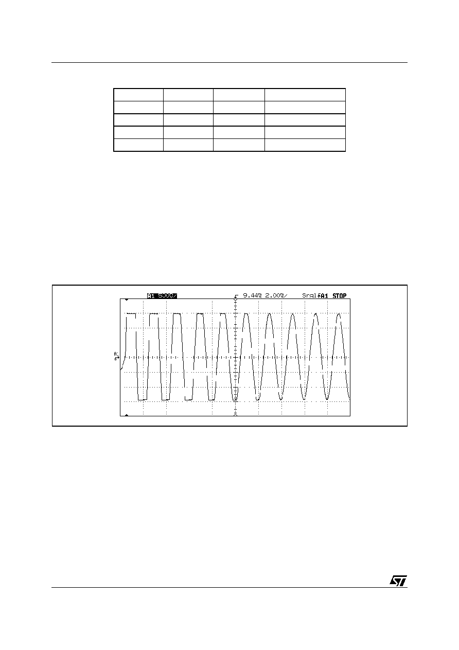
Table 2. DDX gain
DDX Gain Compression
Since a full-scale output of the GC/Vol block is mapped to full output modulation, any signal exceeding 0 dBFS
at the output of the GC/Vol block will be clipped. The purpose of the compression algorithm is to reduce the
gain of the system when 0 dBFS has been exceeded such that clipping does not take place, thus performing an
output limiting function. This would yield a constant Vout once the gained input exceeds 0 dBFS.
With DDX_GAIN_0 = 1, the output of the GC/Vol block is compared to a threshold set just below 0 dBFS. When
the output of GC/Vol exceeds this threshold the gain of system is reduced following a set time-constant and
gain-reduction rate. This reduction in gain is stored as a variable. If subsequently the output of GC/Vol remains
below a separate lower threshold for a set amount of time the gain is then increased following another time-
constant and gain rate. Thus, seven different constants determine the attack, release, and limiting characteris-
tics of the compression algorithm. These constants have been tuned to sound as musical as possible when the
dynamic range of a recording is being reduced due to 0 dBFS being exceeded.
Figure 15. Compression response to 500 Hz sine at 0 dBFS with gain of +10 dB
DDX_GAIN_0
DDX_GAIN_1
DDXGain
DDX Compression
0
0
1x
NO
0
1
2x
NO
1
0
2x
YES
1
1
3x
YES

STA304
26/30
13.10Configuration Register B (CRB) : add. 5Ch
NOTE: Power-on default values will configure serial input interface as I2S Slave and the output interface as I2S Master.
D15
D14
D13
D12
D11
D10
D9
D8
D7
D6
D5
D4
D3
D2
D1
D0
I2SO_M
SbLSb
I2SO_LR
CK_Master
I2SO_LR
CK_Pol
I2SO_BC
K_Master
I2SO_BI
CK_Pol
I2SO_Ali
gn_2
I2SO_Ali
gn_1
I2SO_Ali
gn_0
I2SI_MS
bLSb
I2SI_LR
CK_Master
I2SI_LR
CK_Pol
I2SI_BC
K_Master
I2SI_BIC
K_Pol
I2SI_Alig
n_2
I2SI_Alig
n_1
I2SI_Alig
n_0
BIT
R/W
RST
NAME
DESCRIPTION
0
R/W
1
I2SI_Align_0
I2S (Input) Alignement. Using these bits the word alignement can be
adjusted with respect to the LRCK edges. Please refer to the related
paragraph for more details. The default value is mode 1.
1
R/W
0
I2SI_Align_1
2
R/W
0
I2SI_Align_2
3
R/W
1
I2SI_BICK_Pol
I2S (Input) BICK Polarity. This bit should be configured according to the
used serial protocol. In order to sample incoming data on the rising
edge (data changes on the falling edge) this bit should be set to 1. Set
to 0 to reverse the sampling edge.
4
R/W
0
I2SI_BCK_Master
I2S (Input) Master/Slave Selection. The I2S input interface can be
configured as both master or slave: if the master mode is selected (1)
the BICK line will be an output (64 x 48KHz fixed). Otherwise (0) slave
mode is selected and this line is an input.
5
R/W
0
I2SI_LRCK_Pol
I2S (Input) LRCK Polarity. Set to 0 to receive LEFT samples when
LRCK is low, 1 otherwise.
6
R/W
0
I2SI_LRCK_Master
I2S (Input) Master/Slave Selection. The I2S input interface can be
configured as both master or slave: if the master mode is selected (1)
the LRCK line will be an output (48KHz fixed). Otherwise (0) slave mode
is selected and this line is an input (continuous frequency between
32KHz and 96KHz).
7
R/W
1
I2SI_MSbLSb
I2S (Input) MSb/LSb Selection. Use this bit to select how the sample word is
received by the I2S input interface: set to 0 to configure as LSb first, 1 MSb first.
8
R/W
1
I2SO_Align_0
I2S (Output) Alignemt. Using these bits the word alignement can be
adjusted with respect to the LRCK edges. Please refer to the related
paragraph for more details. The default value is mode 1.
9
R/W
0
I2SO_Align_1
10
R/W
0
I2SO_Align_2
11
R/W
1
I2SO_BICK_Pol
I2S (Output) BICK Polarity. This bit should be configured according to
the used serial protocol. In order to sample outcoming data on the rising
edge (data changes on the falling edge) this bit should be set to 1. Set
to 0 to reverse the sampling edge.
12
R/W
1
I2SO_BCK_Master
I2S (Output) Master/Slave Selection. The I2S output interface can be
configured as both master or slave: if the master mode is selected (1)
the BICK line will be an output (64 x 48KHz fixed). Otherwise (0) slave
mode is selected and this line is an input.
13
R/W
0
I2SO_LRCK_Pol
I2S (Output) LRCK Polarity. Set to 0 to transmit LEFT samples when
LRCK is low, 1 otherwise.
14
R/W
1
I2SO_LRCK_Master
I2S (Output) Master/Slave Selection. The I2S output interface can be
configured as both master or slave: if the master mode is selected (1)
the LRCK line will be an output. Otherwise (0) slave mode is selected
and this line is an input. In any case the frequency is fixed at 48 kHz
15
R/W
1
I2SO_MSbLSb
I2S (Output) ) MSb/LSb Selection. Use this bit to select how the sample
word is transmitted by the I2S output interface: set to 0 to configure as
LSb first, 1 MSb first.

STA304
27/30
13.11Phantom Center Register (add. 60h)
Setting bit 0 enables the phantom center channel feature. When this feature is on, the content of the center
channel is split and added to the L and R channels.
13.12Static EQ and Side Firing Register (add. 70h)
This register controls the activation of the Static EQ and the Side Firing surround sound.
For more information on setting EQ parameters, see Paragraph 9 .2
13.13Bass Management Register (add. 72h)
Setting bit 0 activate the Bass Management. For more information on Bass Management, see Paragraph 9 .1.
Default is 0h.
13.14Bypass Register (add. 74h)
Setting bit 0 bypass the DSP block. All channels are bypassed and output equal to input, regardless of all other
algorithm register settings (Volume, Tone, Phantom, EQ). Default is 0h
D15
D14
D13
D12
D11
D10
D9
D8
D7
D6
D5
D4
D3
D2
D1
D0
Phantom
D15
D14
D13
D12
D11
D10
D9
D8
D7
D6
D5
D4
D3
D2
D1
D0
EQ1
EQ0
EQ1
EQ0
0
0
EQ off (default)
0
1
EQ enabled
1
x
Side Firing + EQ
D15
D14
D13
D12
D11
D10
D9
D8
D7
D6
D5
D4
D3
D2
D1
D0
Bass
Mng
D15
D14
D13
D12
D11
D10
D9
D8
D7
D6
D5
D4
D3
D2
D1
D0
Bypass

STA304
28/30
13.15BIST and Status Register (BASR) : add. 76h
13.16Coefficients Handling Registers (add. 78h ≠ 7Ah)
See paragraph 10.
13.17Vendor ID Registers (add. 7Ch ≠ 7Eh)
These registers are specific vendor identification for the STA304. The Microsoft's Plug and Play Vendor ID code is "ALJ". The REV7..
0 field is for the Vendor Revision number. These are read only registers, any write request to one of these will be ignored.
D15
D14
D13
D12
D11
D10
D9
D8
D7
D6
D5
D4
D3
D2
D1
D0
DSP_BIS
T_Start
DSP_BIS
T_Running
DSP_BIS
T_Stop
DSP_RA
M
X
X
SRC_SP
RAM_2
SRC_SP
RAM_1
DDX_DP
RAM
DDX_SP
RAM_3
DDX_SP
RAM_2
DDX_SP
RAM_1
BIST_St
op
BIST_St
art
SPDIF_
Status
SRC_St
atus
BIT
I/F
DSP
RST
NAME
DESCRIPTION
0
R
1
SRC_Status
When 0, the digital pll in the SRC is LOCKED. When 1 the digital
PLL is OUT of LOCK.
1
R
1
SPDIF_Status
When 1, the SPDIF interface is out of lock. When 0 the interface
is locked to the SPDIF stream input.
2
W
R
0
BIST_Start
Reserved
3
R
0
BIST_Stop
Reserved
4
R
0
DDX_SPRAM_1
Reserved
5
R
0
DDX_SPRAM_2
Reserved
6
R
0
DDX_SPRAM_3
Reserved
7
R
0
DDX_DPRAM
Reserved
8
R
0
SRC_SPRAM_1
Reserved
9
R
0
SRC_SPRAM_2
Reserved
10
R/W
1
AC3_AMEN
Enable automuting if AC3 frame header found
11
R/W
0
CH1_AMEN
Enable automuting if no CH1_STATUS bit found
12
R
R
0
DSP_RAM
Reserved
13
R
R
0
DSP_BIST_Stop
Reserved
14
R
R
0
DSP_BIST_Running
Reserved
15
W
R
0
DSP_BIST_Start
Reserved
D15
D14
D13
D12
D11
D10
D9
D8
D7
D6
D5
D4
D3
D2
D1
D0
C15
C14
C13
C12
C11
C10
C9
C8
C7
C6
C5
C4
C3
C2
C1
C0
AD7
AD6
AD5
AD4
AD3
AD2
AD1
AD0
R/W
C19
C18
C17
C16
D15
D14
D13
D12
D11
D10
D9
D8
D7
D6
D5
D4
D3
D2
D1
D0
0
1
0
0
0
0
0
1
0
1
0
0
1
1
0
0
0
1
0
0
1
0
1
0
REV7 REV6 REV5 REV4 REV3
REV2
REV1
REV0

29/30
STA304
TQFP44 (10 x 10)
DIM.
mm
inch
MIN.
TYP.
MAX.
MIN.
TYP.
MAX.
A
1.60
0.063
A1
0.05
0.15
0.002
0.006
A2
1.35
1.40
1.45
0.053
0.055
0.057
B
0.30
0.37
0.45
0.012
0.014
0.018
C
0.09
0.20
0.004
0.008
D
12.00
0.472
D1
10.00
0.394
D3
8.00
0.315
e
0.80
0.031
E
12.00
0.472
E1
10.00
0.394
E3
8.00
0.315
L
0.45
0.60
0.75
0.018
0.024
0.030
L1
1.00
0.039
K
0∞
(min.), 3.5∞(typ.), 7
∞
(max.)
A
A2
A1
B
Seating Plane
C
11
12
22
23
33
34
44
E1
E
D1
D
e
1
K
B
TQFP4410
L
0.10mm
.004
OUTLINE AND
MECHANICAL DATA

Information furnished is believed to be accurate and reliable. However, STMicroelectronics assumes no responsibility for the consequences
of use of such information nor for any infringement of patents or other rights of third parties which may result from its use. No license is granted
by implication or otherwise under any patent or patent rights of STMicroelectronics. Specifications mentioned in this publication are subject
to change without notice. This publication supersedes and replaces all information previously supplied. STMicroelectronics products are not
authorized for use as critical components in life support devices or systems without express written approval of STMicroelectronics.
The ST logo is a registered trademark of STMicroelectronics
Æ
2002 STMicroelectronics - All Rights Reserved
DDX is a trademark of Apogee Technology inc.
STMicroelectronics GROUP OF COMPANIES
Australia - Brazil - Canada - China - Finland - France - Germany - Hong Kong - India - Israel - Italy - Japan -Malaysia - Malta - Morocco -
Singapore - Spain - Sweden - Switzerland - United Kingdom - United States.
http://www.st.com
30/30
STA304